Transmission Lines from Nets
The Signal Integrity (SI) problem generally requires the construction of transmission lines. The net statement, typically used for constructing electrical net lists, lacks some nuance in this regard. With net connections, there is no ordering of the connection between pads. By the time we get to the board view tool, the user is on their own to get the transmission line right. Ordering of components, trace widths, and clearances become details to manage. Consistency is a goal that is difficult to achieve. Maintaining this kind of consistency is a challenge in many EDA tools.
JITX's solution to this problem revolves around defining additional constraints that layer on top of the net statement. These constraints typically come in two forms:
- Medium Independent Constraints - ordering of pads (topologies), widths of traces, etc.
- Medium Dependent Constraints - timing delays, insertion loss limits, etc.
The JITX's current implementation of SI constraints is limited but will expand over time.
What is a Topology?
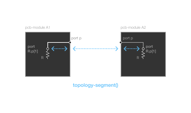
In JITX, a "Route Topology" (usually shorted to topology) is an ordered set of connections between component pads. You can think of the topology as a tree where the edges are the "Topology Segments" and the nodes are physical component pads. Each node can attach to 1 or more segments.
Note that we said ordered, but not directed. There is no connotation of input or output, transmitter or receiver, applied to the endpoints or nodes of the topology tree.
The "Route Topology" tree is acyclic by definition. If we have nodes A, B, C, and D, then we can construct a topology A => B => D or we can construct A => C => D. But we can't construct a topology that routes A => D by two parallel B and C routes in the same topology.
For example:
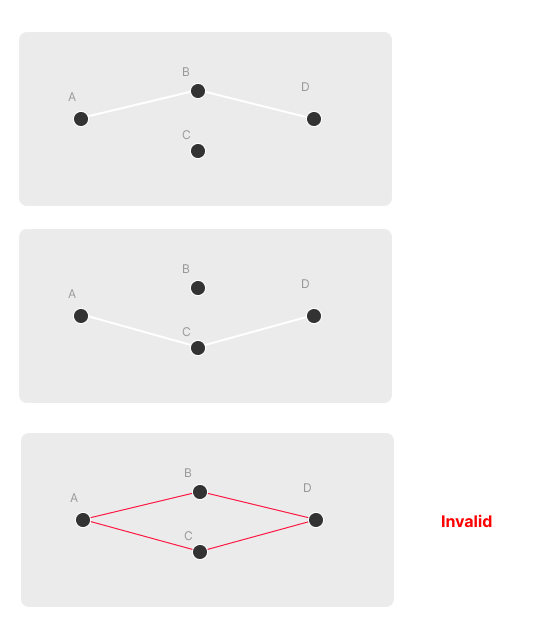
In other words, there can only be one path from A to D.
Valid Topology
A topology can be consider valid or invalid. Sometimes it is not trivial to make this determination due to Pin Assignment.
Requirements
- Each segment of a topology must have both:
- A net statement.
- A topology-segment statement.
- Each node of a topology must associate with a physical pad.
- This means a component port - not a module port.
- See Module Port Forwarding for more info.
- Pass through components (like resistors or blocking capacitors) need a pin-model statement.
Invalid Segments
A "Invalid Segment" refers to any segment of a topology that does not have both a topology-segment and net statement associated with it.
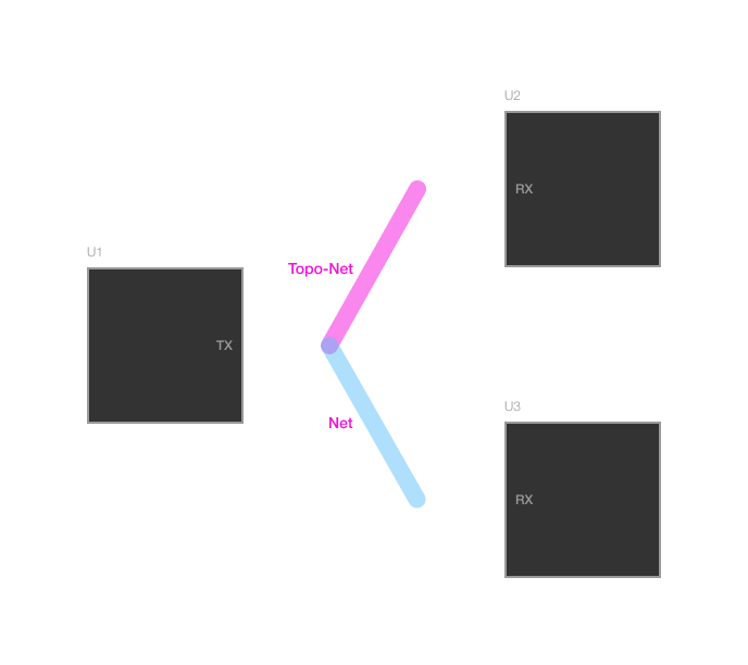
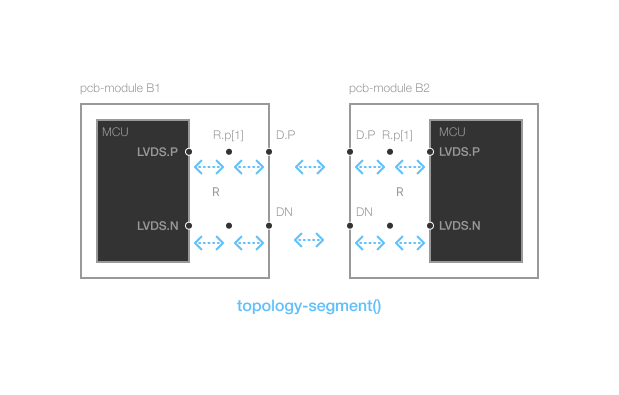
In this example, notice that the segment from U1.TX to U2.RX is a proper segment with a topology-segment and net statement. In short hand, we typically call this a topo-net.
The segment from U1.TX to U3.RX only has a net statement. This "appendage" net causes this topology to contain an invalid segment. When the routing engine encounters this topology, it can't properly define the constraints and labels it as invalid.
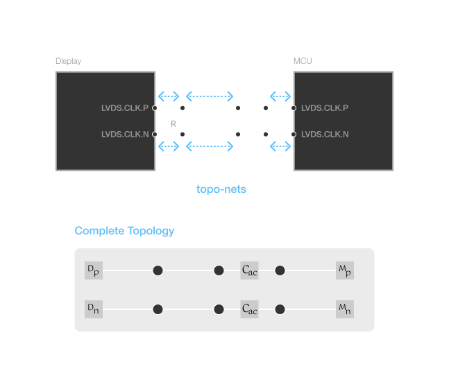
Circuit Topology
In most real-world signal integrity circuits, we typically don't have just copper traces. There are typically various components like capacitors, ESD protection diodes, common-mode chokes, among others that are part of the complete signal topology.
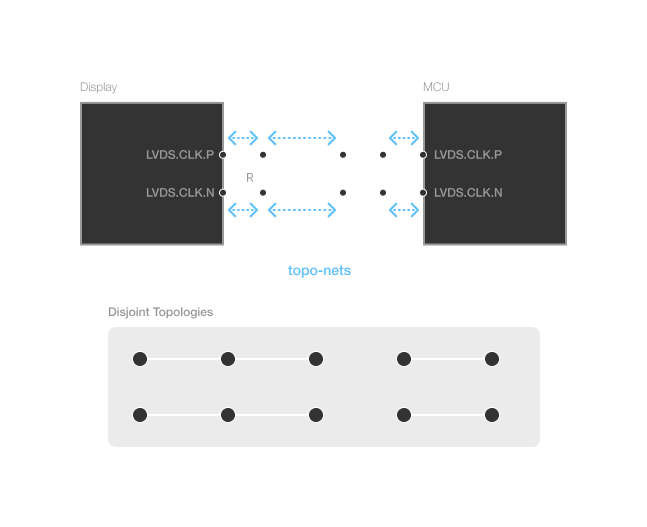
In the diagram above, the small circles are the nodes of the topologies, and the blue dotted arrows represent the topo-nets.
Here we see some common component examples - termination resistors and AC blocking caps. The insertion of these components causes our topology to become disjointed. Let's say we wanted to apply a timing-difference constraint between the signals of the differential pair between MCU and Display. These disjointed topologies present a bit of a problem. For example, we might need a much more complicated constraint, like constraining the sum of the lengths of two pairs of topologies. But this would mean that compensating skew dynamically becomes basically impossible.
This is where the pin-model comes in. The pin-model creates the link between disjointed routing topologies that utilize "pass-through" components.
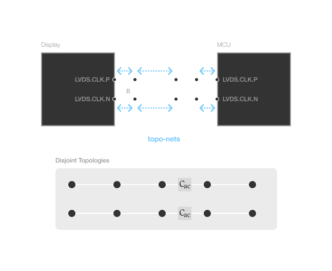
By adding a pin-model statement to the AC blocking capacitors, we collapse the 4 disjoint routing topologies into 2 circuit topologies. In this case, we've used the "Pass-Through" form of the pin model. This form provides a mechanism for defining how the signal flows from one node of a topology to another node of a different topology.
Notice that we don't have to add pin models on every component. As shown, the termination resistor doesn't have a pin-model. This often can be useful when we don't want to introduce cycles or multiple ambiguous paths in a topology.
With the models in place, there is a contiguous path from one endpoint MCU.LVDS.CLK.P to Display.LVDS.CLK.P (and similarly for the N side of the differential pair). Now we can add constraints between the two endpoints of these signals without issue.
Endpoint Pin Models
In addition to the "Pass-Through" pin models for components like resistors and capacitors, each endpoint may provide a "Single-Ended" pin model. These models characterize the delay and loss from the silicon through the wire-bonding and out the package via its pins. In complex chips, this delay and loss may be different from one pin to another.
These models are not strictly necessary. If they are not provided, then the routing engine will just assume all pads have zero delay and loss.
To complete the circuit topology, we can include these pin models in our design:
These "Single-Ended" models are added with the pin-model statement. We add one model for each of the physical component pads. The routing engine can then use this information to correctly compute delay and loss constraints for the entire topology.
Circuit Topology Realization
Realization is the process by which the abstract information of the circuit is formed into physical copper geometry in the board. This process has to take into account various clearance, width, and other requirements. It is where the rubber meets the road. The routing engine can either construct a circuit at this point - or it can't and fails.
In the context of the SI topology, realization is affected by the choice of nodes and segments. One way that it affects realization is by the means of "Stubs."
Consider this circuit - an excerpt of which is shown below:
pcb-module top-level :

  inst A : resistor-model
  inst B : resistor-model
  inst C : resistor-model


  net (A.p[1], B.p[1])
  topology-segment(A.p[1], B.p[1])
  structure(A.p[1] => B.p[1]) = single-ended

  net (B.p[1], C.p[1])
  topology-segment(B.p[1], C.p[1])
  structure(B.p[1] => C.p[1]) = single-ended
This is a simple topology consisting of two segments and three nodes.
Here is a reasonable expectation for how this might realize:
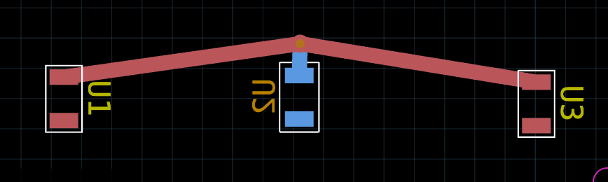
In this rendering:
* A => U1
* B => U2
* C => U3
I've placed B on the bottom layer and hence it requires a via.
The choice of how to place the via is where things get tricky. The order of operations matters.
Order Matters
When we drag out the via for the connection, we can do so by dragging the via from A.p[1] or from B.p[1] (we could also do C but in this case, it is symmetric with A). In the following video, I drag the via from B.p[1]
In this case, the "Stub" is the copper from the via to B.p[1]. Because the via was dragged out from a pad on B, the via is associated with B. If we were to move the B component, the via would move with it. The routing engine considers the via an extension of the B component.
That is what allows us to select A.p[1], the via, and C.p[1] and successfully route the signal topology. The via is effectively B.p[1].
Now - what if dragged the via out from A.p[1] instead of B.p[1]:
On the surface, it would seem like these are exactly the same. But there is an important difference. Because the via was dragged out from A.p[1], the via is now associated with the A component. If we moved A, the via would move with it. For the connection between A.p[1] and B.p[1], this association has no effect. We can still connect B.p[1] to the via. But the "Stub" has moved - the stub is now A.p[1] to the via.
This presents problems for connecting to C.p[1]. Because the via is a stub for A.p[1], we can't connect the via directly to C.p[1]. This would violate the constraints of the topology. The runtime prevents this connection because it is technically a circuit inconsistent with what is described in code. Hence the blue "There are no valid connections..." banner.
This phenomenon will apply equally to control points as well.
Module Port Forwarding
In JITX we can use pcb-module definitions to create sub-circuits and reusable designs. We use the same port terminology for both pcb-module and pcb-component to describe the inputs and outputs to a circuit or component. But the ports of a pcb-module are different from the ports of a pcb-component.
The ports in a component map to a physical pad in a land pattern. This means that there is a physical manifestation of a component port in the PCB. The ports of a module don't necessarily have a 1:1 mapping from port to pad. This causes a bit of an issue when attempting to define a topology. If the module port maps to 3 physical pads, then should the topology create a branching tree? Should the topology connect to them serially? What do we do about amibiguities?
Simple Topology
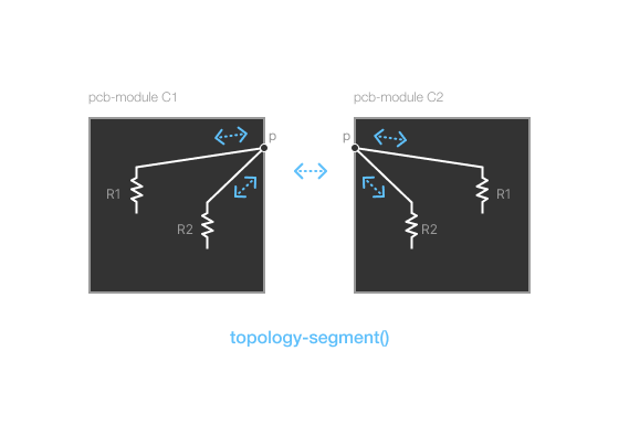
We're going to start off with a base case for demonstrating how topologies and modules work together. In this example we have two sub-circuits that we instantiate and connect together:
pcb-routing-structure se-50:
  ...

pcb-module A:
  port p : pin

  inst R : resistor-model

  net (p, R.p[1])
  topology-segment(p, R.p[1])

pcb-module parent:

    inst A1 : A
    inst A2 : A

    net (A1.p, A2.p)
    topology-segment(A1.p, A2.p)

    structure(A1.p, A2.p) = se-50
Here is a visual representation of this topology:
There are technically 3 topology-segment statements in this design. But because pcb-module ports are different - we really only have one topology-segment. When a module port connects to one and only one component port, the module port "forwards" to the component port. In this example, the port p on module A forwards to R.p[1].
This "forwarding" concept is is important because this allows us to use the structure statement at the top level to apply the single-ended 50 ohm trace to the entirety of the topology. If we did not have this forwarding mechanism, then we would have to pass the routing structure in to the sub-circuit like this:
; More complicated arguments to the module
pcb-module A (rte:RoutingStructure):
  port p : pin

  inst R : resistor-model

  net (p, R.p[1])
  topology-segment(p, R.p[1])
  ; Explicit structure statement inside
  ;  each module.
  structure(p, R.p[1]) = rte
This is not conducive to making re-usuable subcircuits. Having to pass in the routing structure means that it must propagate to any sub-circuits in the same way. The forwarding mechanism allows us to avoid this complexity.
Bundles & More Components
Let's consider a more complex module example.
For this example, I'm going to transition to using JSL's SI helper routines for a more concise representation.
Naive Approach
We're going to start with a straight forward approach where we just connect topologies in a logical way:
import jsl/si/helpers
import jsl/bundles
pcb-differential-routing-structure diff-100:
...
pcb-module B:
port D : diff-pair
; Termination Resistor
inst R : resistor-model
inst MCU : some-MCU-with-LVDS
topo-net(D.P => R.p[1] => MCU.LVDS.P)
topo-net(D.N => R.p[2] => MCU.LVDS.N)
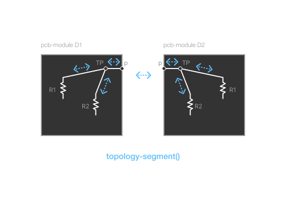
pcb-module parent:
inst B1 : B
inst B2 : B
topo-net(B1.D => B2.D)
diff-structure(diff-100, B1.D => B2.D)
Here is a visual representation of this topology:
First, notice that our topology inside the sub-module B consists of a chain of connections from the port D to the port MCU.LVDS. We've effectively added a termination resistors between D and MCU.LVDS. By adding this node in the topology, we still have a single 1:1 module port to component port mapping.
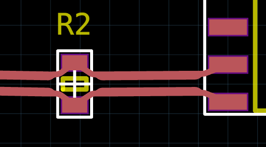
If we look at how this design realizes in our circuit - we'll see something unexpected:
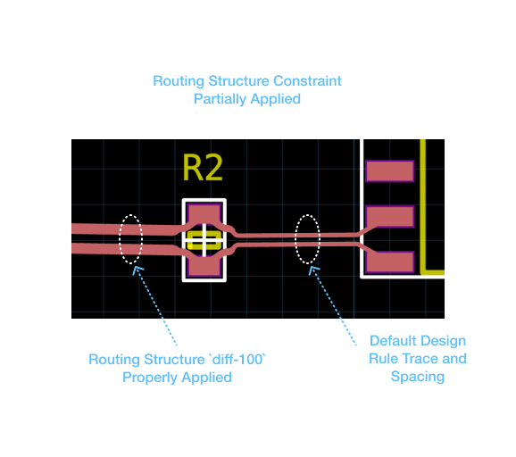
Notice how the diff-100 differential structure gets applied on the trace to the left of the resistor R but does not get applied to the traces from the R to the MCU. The issue is that the module port forwarding only extends to R. This means that when diff-structure is called, the port B1.D.P forwards to R.p[1] only and that becomes the endpoint of the constraint application.
Constraining the entire topology
Let's try to address these issues with a slight refactor:
import jsl/si/helpers
import jsl/bundles

pcb-differential-routing-structure diff-100:
  ...

pcb-module B:
  port D : diff-pair

  ; Termination Resistor
  inst R : resistor-model

  public inst MCU : some-MCU-with-LVDS

  topo-net(D.P => R.p[1] => MCU.LVDS.P)
  topo-net(D.N => R.p[2] => MCU.LVDS.N)

pcb-module parent:

  inst B1 : B
  inst B2 : B

  topo-net(B1.D => B2.D)
  diff-structure(diff-100, B1.MCU.LVDS => B2.MCU.LVDS)
The topology representation hasn't changed, but we've modified the constraint application. In order to apply the differential routing structure diff-100 to the segment from R to MCU.LVDS, I need to make the MCU instance public. Then from the parent context I can reference into B1 and B2 to set the true endpoints of the topology.
Now when we route the design we see:
This isn't optimal either. It requires the user of this module to understand the inner workings of the B module. But it serves to demonstrate one of the limitations of the module port forwarding mechanism. For a more robust solution to this problem, see Signal Ends.
An Invalid Topology with a Module
In the previous example, we added components to the design while preserving the 1:1 mapping of the module port to a component port. Now let's see what happens when we violate this requirement:
pcb-module C:
  pin p

  inst R1 : resistor-model
  inst R2 : resistor-model

  ; This creates a Y structure in the
  ;   topology graph.
  topo-net(p => R1.p[1])
  topo-net(p => R2.p[1])

pcb-module parent:

  inst C1 : C
  inst C2 : C

  topo-net(C1.p => C2.p)
Here is a visual representation of this invalid topology:
Notice how in this example, the port module p connects to one pin on each of R1 and R2. This causes a bit of ambiguity with respect to how the port p maps to a physical component pad. In this simple example, it isn't as obvious to see why a Y junction can't be created in this case. But this does violate the 1:1 module port to component port assumption. That assumption makes the logic and realization of these topologies easier as the circuits become more complex.
Fixing the Ambiguity
pcb-component test-point:
  port tp : pin
  ...

pcb-module D:
  port p : pin

  inst TP : test-point

  topo-net(p => TP.tp)

  inst R1 : resistor-model
  inst R2 : resistor-model

  topo-net(TP.tp => R1.p[1])
  topo-net(TP.tp => R2.p[1])

pcb-module parent:

    inst D1 : D
    inst D2 : D

    topo-net(D1.p => D2.p)
Here is a visual representation of this topology:
By inserting the test point component, we can control the 1:1 relationship and still achieve the Y structure for the topology.
Notice that this circuit has 7 topology-segment() statements but it has only 1 topology. That topology has 5 total segments:
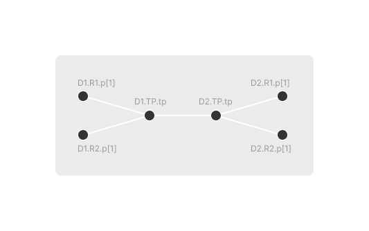
Notice that the module ports don't exist in this topology. They effectively dissolve away as the topology is realized in the PCB.
Mental Model Recap
The mental model for the SI topology system consists of two trees:
- The Circuit Topology Tree
- This is a tree consisting of many disjoint, ordered sub-graphs (Route Topologies)
- The nodes of this graph are the component ports - not the module ports.
- The edges of this graph are the
topo-nets - The Realization Tree
- This is the tree of traces, vias, and component pads that realizes one of the Route Topologies.
- The nodes of this tree are:
- Component Pads
- Vias
- Control Points
- The edges of this tree are the copper traces
- The features of these trace are defined by Routing Structures.
- The allowed paths of these traces are defined by the topology.
What's Next: Let's talk about constraints.