Materials
A pcb-material definition represents a material in a pcb-stackup layer.
Signature
pcb-material mat-name (arg1:Type1, ...) :
  name = <String|False>
  description = <String|False>
  type = <MaterialType>

  material-name = <String|False>

  ; For Dielectric Materials
  dielectric-coefficient = <Double|False>
  loss-tangent = <Double|False>

  ; For Conductor Materials
  roughness = <Double|False>
The expression name mat-name uniquely identifies this stackup definition in the current context.
The argument list (arg1:Type1, ...) is optional and provides a means of
constructing parameterized material definitions.
- Required Parameters
type- There are two valid values forMaterialTypeConductorDielectric
- Optional Parameters
name- This name is used in the UI as a more user friendly name. If this string is not provided then themat-nameexpression is used as the stackup's name.description- This string is defining more meta-data for the material - such as manufacturer of this material.material-name- This string label is optional and used only for Kicad Import/Export.DielectricType Optional Parametersdielectric-coefficient- Relative Coefficient of Permittivity for this material. This value is a unit-less instance of typeDoubleand generally should be 1.0 or greater.loss-tangent- The Loss Tangent for this material. This value is a unit-less instance of typeDouble.
ConductorType Optional Parametersroughness- Surface Roughness of the conductor layer. This parameter effects the losses in RF circuits due to the skin effect. This value is in mm.
If you add roughness to a Dielectric type or a loss-tangent to a Conductor type, the JITX runtime will throw an error.
Example:
Uncaught Exception: Dielectrics can only have dielectric-coefficient and loss-tangent attributes.
Usage
The pcb-material statements create definitions that are primarily used by the pcb-stackup statement. These material definitions provide the properties of each material in the stackup.
Below is a trivial example for a 2-layer board:
pcb-material core-45 :
  type = Dielectric
  dielectric-coefficient = 4.5
  loss-tangent = 0.008

pcb-material soldermask :
  type = Dielectric
  dielectric-coefficient = 3.2
  loss-tangent = 0.012

pcb-material copper:
  type = Conductor

pcb-stackup simple-2-layer :
  name = "2-layer 1.6mm"
  stack(0.019, soldermask)
  stack(0.035, copper)
  stack(1.5, core-45)
  stack(0.035, copper)
  stack(0.019, soldermask)
Using Arguments
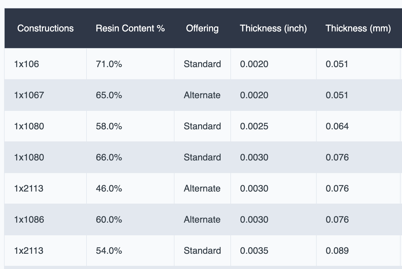
Often times, a family of prepreg materials will come in multiple different constructions. For example, see Isola 370HR. Here is an excerpt from their core data:

We might want to construct a pcb-material that allows us to label with these different features:
pcb-material isola-370HR (ply:String, Dk:Double, Df:Double) :
  name = to-string("Isola 370HR %_" % [ply])
  type = Dielectric
  dielectric-coefficient = Dk
  loss-tangent = Df

val isola-370hr-1080 = isola-370HR("1x1080", 4.04, 0.021)
This structure allows us to build a material spec for any
of the cores in the Isola catalog. The name for this material will be Isola 370HR 1x1080 which we can use in programmatically generated stackup tables.