Layer
The layer statement is used to create geometry on the non-copper layers of a circuit board. The layer() statement is valid in the following contexts:
Signature
layer(<LayerSpecifier>) = <Shape>
<LayerSpecifier>- A LayerSpecifier instance that identifies which non-copper layer to apply the provided geometry to.<Shape>- AShapeinstance that defines the geometry that will be created on the specified layer.
Usage
The most common usage of the layer() statement is in pcb-landpattern:
pcb-landpattern diode-lp :
  pad c : smd-pad(0.4, 0.75) at loc(-1.25, 0.0) on Top
  pad a : smd-pad(0.4, 0.75) at loc(1.25, 0.0) on Top

  layer(Silkscreen("body", Top)) = LineRectangle(1.8, 1.0)
  layer(Silkscreen("body", Top)) = Line(0.1, [Point(-0.70, -0.5), Point(-0.70, 0.5)])
  layer(Courtyard(Top)) = Rectangle(3.2, 2.0)

  layer(ForbidCopper(LayerIndex(0))) = Rectangle(2.0, 1.0)
This will construct a landpattern that looks like this:
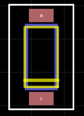
Notice the silkscreen in yellow with cathode marker. The blue box is the ForbidCopper layer on the Top Layer. Red is the top copper pads for the cathode c and anode a.
The white bounding rectangle is the Courtyard layer.
See LayerSpecifier for more information about specific layers.
Cutouts
When constructing cutouts in the board layout, your best bet is to use a solid region as opposed to a line. A line can confuse the routing engine into thinking that there are two physically separate regions where copper can be placed.
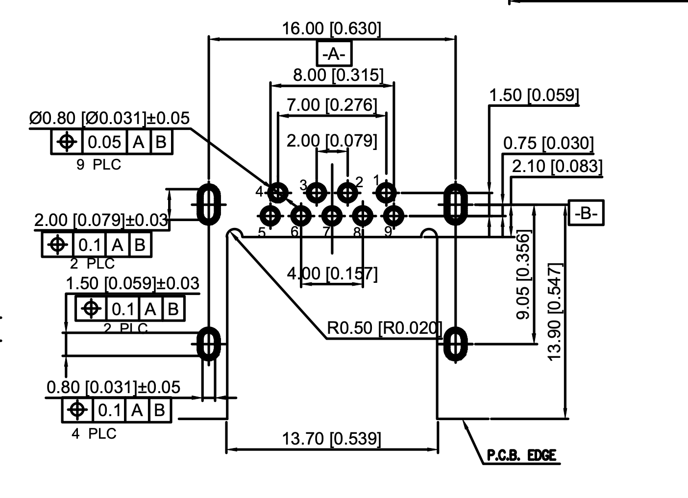
Consider a USB connector part, U231-096N-3BLRT06-SS, Jing Extension of the Electronic Co.
Here is an excerpt from the datasheet:
If we draw the cutout with a line, as shown in the datasheet, we get this:
pcb-landpattern USB-conn:
  ...

  layer(Cutout()) = Line(0.254, [Point(-7.300, -7.650), Point(-8.450, -7.650)])
  layer(Cutout()) = Polyline(0.254, [
    Point(6.850, 4.650)
    Point(6.850, -7.650)
    Point(8.450, -7.650)])
  layer(Cutout()) = Polyline(0.254, [
    Point(-6.850, 4.650)
    Point(-6.850, -7.650)
    Point(-7.300, -7.650)])
  layer(Cutout()) = Line(0.254, [Point(-6.850, 4.650), Point(6.850, 4.650)])
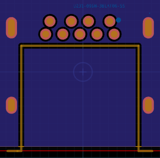
The cutout line is in gold color. Notice that the ground layer (blue) copper is present on both sides of the cut line with some margin in between. The routing engine basically thinks that the cutout is just the line. If we were making a slot - that would probably be reasonable. But for this case, we want the hole region between the cutout line and the board edge (red) to be a cutout region.
The right way is to use a Rectangle or Polygon solid geometry:
pcb-landpattern USB-conn :
  ...

  layer(Cutout()) = Polygon([
    Point(-6.850, 4.650), Point(6.850, 4.650),
    Point(6.850, -7.650), Point(-6.850, -7.65),
  ])
  layer(Cutout()) = Circle(Point(-6.85 + 0.5, 4.65), 0.5)
  layer(Cutout()) = Circle(Point(6.85 - 0.5, 4.65), 0.5)
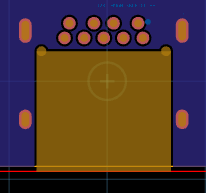
Notice that the cutout region fills the entire connector region and the blue ground plane is not present in the cutout region.
Courtyards
When constructing component courtyards for the board layout, it is preferable to use a solid filled shape, e.g. Rectangle, as opposed to a thin outline, e.g. Line. The board view will calculate and render only the outline of this shape. However, for layout placement and routing and other physical considerations the courtyard will still be the filled shape. For example, using a filled shape ensures the auto-placer will not place other components within the courtyard. A filled courtyard shape will also be selectable by clicking anywhere inside the shape, whereas a thin courtyard shape will only be selectable by clicking exactly on the line itself (or by using area select).