pcb-differential-routing-structure
The pcb-differential-routing-structure is a statement for defining the geometric constraints of a differential pair topology. This definition applies to only the coupled region of a differential pair.
Outline
pcb-differential-routing-structure struct-name (arg1:Type1, ...) :
  name = <String>
  description = <String>

  uncoupled-region = <RoutingStructure>

  layer-constraints(<LayerIndex|Side>):
    trace-width = <Double>    ; mm
    pair-spacing = <Double>   ; mm
    clearance = <Double>      ; mm
    velocity =  <Double>      ; mm/s
    insertion-loss = <Double> ; dB/mm
    ; Option #1 - DifferentialNeckDown Instance
    neck-down = <DifferentialNeckDown>

    ; Option #2 - Macro Form
    ;  Notice the `:` instead of `=`
    neck-down:
      trace-width = <Double>
      pair-spacing = <Double>   ; mm
      clearance = <Double>      ; mm
      velocity =  <Double>      ; mm/s
      insertion-loss = <Double> ; dB/mm

  layer-constraints(<LayerIndex|Side>):
    ...
The routing structure requires an expression name struct-name that uniquely identifies this statement within the current context.
The arguments list (arg1:Type1, ...) is optional and provides a means to parameterize routing structures for common statements.
The name and description properties are optional and are primarily for documentation and labeling purposes. The name property in particular is typically for UI applications. If a name property is not provided, then the expression name struct-name will be used.
The uncoupled-region property is used to apply a particular single-ended routing structure (ie, a pcb-routing-structure) to the uncoupled regions of a differential pair. This typically applies to via breakouts, fanout from an IC, etc.
The elements of the pcb-differential-routing-structure statement are identified using a layer statement. Each of these layer statements must match with a conductor layer in the pcb-stackup defined for the current board design. Conceptually, the idea is to apply different properties depending on the layer.
The layer-constraints() statement takes an argument of either a Side like Top or Bottom, or a LayerIndex. See LayerIndex for more information.
At each layer specification, the user can list any of these properties:
- Required Properties:
trace-width- Width in mm of both of the diff-pair conductors for any traces on this layer.pair-spacing- Spacing distance between the conductors of the differential pair in mm.velocity- Signal Propagation Velocity (also known as Group Velocity) of the signals on this layer. This is primarily used for timing constraints. This property is in unitsmm/s.insertion-loss- Insertion Loss per unit distance of the signals on this layer.- This property is in units of
dB/mm. - This property is assumed to be at the frequency of interest for this design.
- This property is in units of
- Optional Properties
clearance- Minimum "Net to Net" clearance in mm of the traces on this layer. If not provided, then the default minimum clearances from the design rules will be used. This clearance does not affect thepair-spacingfor the differential pair.neck-down- This property allows the user to specify a special set of routing properties for the neckdown region. It comes in two forms:- Instance Form - the user must assign a DifferentialNeckDown instance.
- Macro Form - the user can provide, directly, statements for
trace-width,pair-spacing,clearance, etc like above.
If these properties are not explicitly provided in the routing structure, then either:
- The default design rules for the board will be consulted for
trace-widthandclearance - If there are timing or loss constraints on this route, but no defined structure information for layers that have traces, then default values will be used for
velocityandinsertion-loss. The current default values are:velocity = 0.15e12 ; mm/sinsertion-loss = 0.002 ; dB/mm
Usage
Below are some typical examples of differential routing structures in action.
Edge Coupled Microstrip
; Define a single-ending routing structure for the
;  uncoupled regions
public pcb-routing-structure se-50 ( w:Double = 0.1048 ) :
  name = "50 Ohm Microstrip"
  layer-constraints(Top) :
    trace-width = w
    clearance = w * 3.0
    velocity = 0.19e12
    insertion-loss = 0.008

  layer-constraints(Bottom) :
    trace-width = w
    clearance = w * 3.0
    velocity = 0.19e12
    insertion-loss = 0.008

val ec-stripline-ph-vel = 0.19e12 ; mm / s @ 1GHz
val ec-stripline-loss = 0.008 ; dB/mm @ 1GHz

public pcb-differential-routing-structure diff-100 :
  name = "100 Ohm differential impedance"

  uncoupled-region = se-50()

  layer-constraints(Top) :
    trace-width = 0.0762    ; mm  -  3mil
    pair-spacing = 0.127     ; mm  -   5mil
    clearance = 0.3         ; mm
    velocity = ec-stripline-ph-vel      ; mm/s
    insertion-loss = ec-stripline-loss  ; dB/mm @ 1GHz

  layer-constraints(Bottom) :
    trace-width = 0.0762    ; mm  -  3mil
    pair-spacing = 0.127     ; mm  -   5mil
    clearance = 0.3         ; mm
    velocity = ec-stripline-ph-vel      ; mm/s
    insertion-loss = ec-stripline-loss  ; dB/mm @ 1GHz
In this example, we define two routing structures - a singled ended 50 ohm version and a differential 100 ohm impedance version. The single-ended routing structure is used for the uncoupled regions of the differential pair due to the uncoupled-region statement.
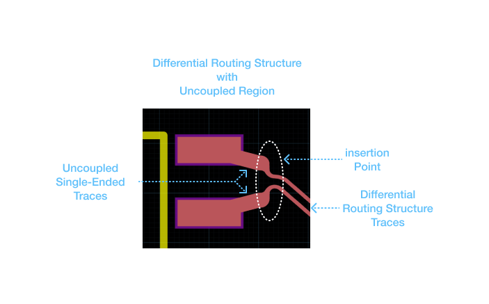
In this example, We've exaggerated the single-ended uncoupled region to make it more visible. The "Insertion Point" is a control point that the user can place to create the transition from the uncoupled regions to the coupled differential pair regions.
Reusing Layer-Constraints Definitions
As we discussed in the single-ended case, we can reuse
the layer-constraints definitions inside a pcb-differential-routing-structure.
In this case we need to define a DiffRoutingStructureLayerConstraints object:
val my-diff-layer-constraints = DiffRoutingStructureLayerConstraints(
  trace-width = 0.18
  pair-spacing = 0.158
  clearance = 0.38
  velocity = 0.18e12
  insertion-loss = 0.0088
  neck-down = DifferentialNeckDown(
    pair-spacing = 0.148
    trace-width = 0.17
    clearance = 0.28
    )
)

pcb-differential-routing-structure my-differential-routing-structure :
  name = "100 Ohm common-mode impedance"
  layer-constraints(Top) = my-diff-layer-constraints
  layer-constraints(Bottom) = my-diff-layer-constraints
  uncoupled-region = my-routing-structure
The generator function method also works, using inside
pcb-differential-routing-structure in place of inside pcb-routing-structure.