Pads
A pcb-pad statement represents a single electrical lead
interface in a pcb-landpattern.
Signature
pcb-pad pad-name (arg1:<Type1>, ...) :
  name = <String>
  description = <String>
  type = <PadType>
  shape = <Shape>
  edge = <True|False>
  layer(<LayerSpecifier>) = <Shape>
The expression name pad-name uniquely identifies this pad definition
in the current context.
The argument list (arg1:Type1, ...) is optional and provides a means of
constructing parameterized pad definitions.
- Required parameters
type- Pad type; eitherSMDorTHshape- Pad shape; aShapeexpression specifying the shape of the copper on all copper layers.- Optional parameters
name- Will be used in place of "pad-name" in the UI if available.description-Stringproviding metadata for thepaddefinition.edge- Sets if the pad is an edge connectorlayer- A layer statement defining the pad's geometry on a non-copper layer of the circuit board.
Usage
Here is a simple example of a parameterized pcb-pad:
a generator for BGA pads of specified diameter:
public pcb-pad bga-pad (diameter:Double) :
  name = "SMD Pad"
  type = SMD

  val radius = diameter / 2.0
  val pad-shape = Circle(radius)

  ; Pad is circular
  shape = pad-shape

  ; Paste layer: Radius 5% smaller
  layer(Paste(Top)) = expand(pad-shape, -(0.05 * radius))

  ; Check current design rules to get soldermask clearance
  val soldermask-amount = clearance(current-rules(), SolderMaskRegistration)

  ; Soldermask layer is larger than pad
  layer(SolderMask(Top)) = expand(pad-shape, soldermask-amount)
Our bga-pad definition constructs circular SMD pads by
computing the pad shape, then adding a slightly larger
circular soldermask layer.
We can use this to build a BGA landpattern.
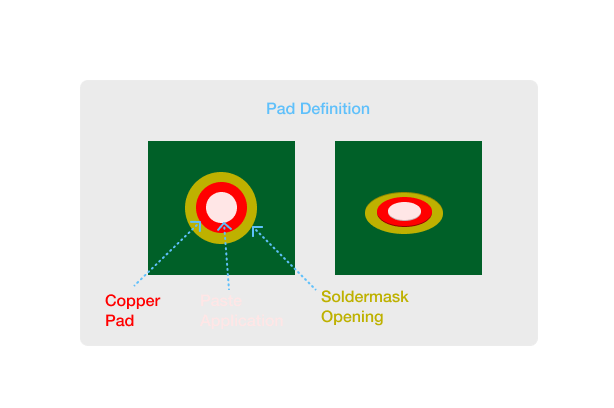
The image below shows the structure of our pad definition:
We use the expand function to construct soldermask outside
of the copper pad, and we reuse it with a negative parameter
to construct a paste layer inside of the pad.
Here is another example, this time of a non-plated through-hole pad:
; Non-plated TH pad
public pcb-pad npth-pad (drill-radius:Double) :
  name = "NPTH-Pad"
  type = TH
  ; Pad is circular
  val hole-shape = Circle(drill-radius)
  shape = hole-shape
  layer(Cutout()) = hole-shape
The type statement specifies that it is a through-hole pad.
The Cutout() layer is the same shape as the pad itself, which
implicitly removes the pad and its plating.
Since it's non-plated we do not need to worry about a paste layer.
We could add a soldermask layer if needed.