Land Pattern
The landpattern statement defines the mapping between the component's ports and the pads of the physical land-pattern.
A pcb-component can have only one associated land-pattern.
Signature
  ; Explicit Mapping Form
  landpattern = <LP>(
    <PORT-1> => <LP>.<PAD-1>,
    <PORT-2> => <LP>.<PAD-2>,
    ...
  )
  ; Pin Properties Table Form
  assign-landpattern(<LP>)
landpattern =statement assigns a landpattern and provides the port to pad mapping explicitly.<LP>- This is a pcb-landpattern definition that will be assigned to the component.<PORT-1>- Refs to individual,SinglePinports of the component<PAD-1>- Refs to individual pads of the<LP>land pattern. Note the use ofdotnotation to specify the pad.- The
=>operator is a mapping operator. assign-landpattern- This is a utility function that leverages the pin-properties table to automate the construction of the port to pad mapping.- The
<LP>is a pcb-landpattern definition
Usage
The landpattern statement is primarily used in two forms:
- Explicit Mapping Form
- Pin Properties Table Form
Explicit Mapping Form
public pcb-component kelvin-resistor :
  manufacturer = "Ohmite"
  mpn = "FC4L16R010FER"

  port p : pin[[1, 2]]
  port sense : diff-pair

  val lp = kelvin-lp
  landpattern = lp(
    self.p[1] => lp.p[1]
    self.p[2] => lp.p[2]
    self.sense.P => lp.p[3]
    self.sense.N => lp.p[4]
  )

pcb-landpattern kelvin-lp :
  pad p[1] : smd-pad(0.45, 1.2) at loc(0.3625, 0.0)
  pad p[2] : smd-pad(0.45, 1.2) at loc(-0.3625, 0.0)
  pad p[3] : smd-pad(0.45, 0.4) at loc(0.3625, 1.1)
  pad p[4] : smd-pad(0.45, 0.4) at loc(-0.3625, 1.1)

  ; More Geometry Here
  ...
When the port names for the component are different from the pad names in the land pattern, we typically need to use the explicit mapping form of the landpattern statement.
This mapping expects the following conditions to be met:
- Each mapping must be from a
SinglePinport to a singlePadon the landpattern. Bundles and PortArrays cannot be mapped with this syntax. - Each component port must have an explicit map. Forgetting a port in the mapping will result in an error.
- Each component port does not necessarily have to be unique. You could have multiple mappings of
GND => p[1],GND => p[2], etc. More on this later. - Each land-pattern pad must be used in only one mapping. If you were to make two mappings with different component ports that both map to
lp.p[1], this will elicit an error.
Pin Properties Table Form
Another way to construct the same component and landpattern mapping would be to use the pin-properties table.
public pcb-component kelvin-resistor :
  manufacturer = "Ohmite"
  mpn = "FC4L16R010FER"

  pin-properties:
    [pin:Ref   | pads:Ref ...]
    for i in 1 through 4 do:
      [p[i]    | p[i] ]

  assign-landpattern(kelvin-lp)

  supports diff-pair:
    diff-pair.P => self.p[3]
    diff-pair.N => self.p[4]
Instead of making an explicit port sense:diff-pair, this version opts to use a supports statement as a means of exposing the differential sense lines of the kelvin resistor. Notice that this version makes no explicit port declarations at all. They are all implicitly defined via the pin-properties table. Upon evaluation, the pin-properties table will create any unknown component ports it finds in the pin column.
In this particular case, the diff-pair supports statement acts more like an interface definition as opposed to a pin-assignment problem. There is only one option for the diff-pair so the solution is trivial. This has the nice benefit of abstracting away what type of component is used to provide the sense interface. For example, it would be easy to swap the kelvin-resistor component with a pcb-module with the same interface but containing a different sensing technique.
One Port to Many Pads
In many electronic components there are multiple pads that map to one functional connection. For example, the ground pin may have 1 or many pads on a component. To support this case, the landpattern statement allows a port ref to be present multiple times. For example in an SMA connector, it is common to have 4 through-hole pads for ground around a center signal pin:
pcb-component SMA :

  port launch : pin
  port gnd : pin

  val lp = SMA-lp
  landpattern = lp(
    launch => lp.p[1],
    for i in 2 through 5 do:
      gnd => lp.p[i]
  )

  val symb = ocdb/utils/symbols/coax-sym
  symbol = symb(
    launch => symb.sig,
    gnd => symb.gnd
    )


pcb-landpattern SMA-lp:
  pad p[1] : pth-pad(0.75, 1.3) at loc(0.0, 0.0)
  pad p[2] : pth-pad(0.8, 1.4) at loc(2.55, 2.55)
  pad p[3] : pth-pad(0.8, 1.4) at loc(2.55, -2.55)
  pad p[4] : pth-pad(0.8, 1.4) at loc(-2.55, 2.55)
  pad p[5] : pth-pad(0.8, 1.4) at loc(-2.55, -2.55)
  ; More Geometry Here
In this example, notice that we use a for-loop to connect the ground pin to the 4 ground through-hole pads of the SMA connector. This has a side effect in the schematic:
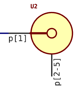
Notice that the ground pin on the coax-symb lists its pads as p[2-5]. This is indicating that the ground symbol maps to pins p[2], p[3], p[4], and p[5].
This syntax is very concise for this simple example. Be warned that this syntax doesn't scale as well when considering, for example, a large FPGA with 10s or 100s of ground pins:
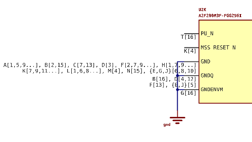
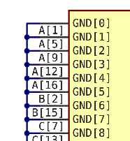
In this case, you will likely be better off constructing a PortArray for the GND port and using individual pad mappings:
pcb-component FPGA:

  pin-properties:
    [pin:Ref | pads:Ref ...]
    [GND[0]  | A[1] ]
    [GND[1]  | A[5] ]
    [GND[2]  | A[9] ]
    ...
This results in a more readable schematic symbol even if it is a bit larger:
Land Pattern Pads are Internal to Components
The land-pattern and its associated pads are not intended to be exposed outside the component. The components ports are the external interface to a component. Any attempt to net to a pad of a component will result in an error.
Notice that in the above examples, the component port and the landpattern pads use the same ref names. So while this may not be unambiguous - know that the port is what we connect to when constructing the circuit and net list.