Copper
The copper statement defines geometry on a specified copper layer of the board stackup.
A copper statement can be used inside
geom statement
in a pcb-module
Signature
copper(<LAYER-INDEX>) = <Shape>
<LAYER-INDEX>- This expects a LayerIndex instance to select which copper layer to apply the created geometry.<Shape>- The geometric Shape to create in this copper layer.
Usage
In the pcb-module context, the copper statement can be used from within a geom statement. The geom statement provides the net to which this copper geometry will be assigned. The most common usage of this statement is defining ground planes or similar geometry with explicit shapes:
val board-shape = Rectangle(30.0, 40.0)

pcb-module top-level:
  ...

  geom(GND):
    val sh = offset{_, -1.0} $ RoundedRectangle(30.0, 10.0, 3.0)
    copper(LayerIndex(0, Bottom)) = loc(0.0, -15.0) * sh
Notice the use of offset to shrink the RoundedRectangle shape by 1mm. The loc function is used to transform the shrunken shape into position in the lower half of the PCB.
Notice the use of offset to shrink the RoundedRectangle shape by 1mm. The loc function is used to transform the shrunken shape into position in the lower half of the PCB.
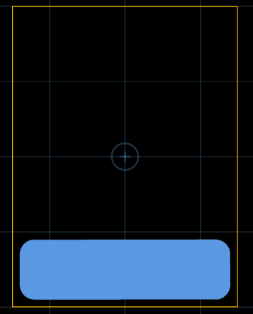
Constructs a shape on the bottom layer with geometry like this:
As a more detailed syntax example, consider these copper statements:
geom(my-net):
  copper(LayerIndex(0)) = Circle(0.0, 15.0, 1.0)
  copper(LayerIndex(1)) = Line(1.0, [Point(0.0, -5.0) Point(5.0, -5.0)])
copper(LayerIndex(0)) = Circle(0.0, 15.0, 1.0)Create a copper circle at (x,y) = (0,15mm) of radius 1mm. You can use any Shape with thecopperstatement.copper(LayerIndex(1)) = Line(1.0, [Point(0.0, -5.0) Point(5.0, -5.0)])Create a 1mm wide copper line (results in a trace) on the 2nd copper layer from the top.