Pin Properties
The pin-properties statement defines a table for quickly and easily constructing the ports for a component. In addition to defining the ports, the pin-properties table can also easily add property statements to each pin in the table. This statement is effectively an automation tool for more easily generating lower level JITX statements.
The pin-properties statement is valid in the pcb-component and pcb-module contexts. Each component or module may contain one or more pin-properties tables.
While you can use pin-properties in the pcb-module context, it is most typically found
in the pcb-component context.
Signature
  pin-properties:
    <HEADER>
    <ROW-1>
    <ROW-2>
    ...
<HEADER>- Defines the schema for each following rows of the pin properties table.<ROW-*>- Each row describes aSinglePinport of this component.
<HEADER> Signature
[ <NAME-1>:<TYPE-1> | <NAME-2>:<TYPE-2> | ... ]
The <HEADER> consists of a fixed-length set of <NAME>:<TYPE> pairs. The <NAME> value defines the name of the property for this table. Commonly used property names include:
pin- This identifies whichSinglePinport of the component that the following properties apply to. This is typically aReftype.pads- This identifies which pads on the land pattern map to a particular. This is typically used with eitherIntorReftype and is often combined with the...operator. See more information below.bank- This identifier is used withIntorReftype to identify the banks of a multi-part symbol.side- This identifier is commonly used with the "Box Symbol" generators. This property is used with theDirtype to indicate which side of the box a pin will be placed on.
Beyond these properties, any identifier and type can be used to add custom properties to ports.
The ... Operator
The ellipsis points operator ... is used in the header to indicate that this column may contain multiple values. This is typically used for the pads identifier to map multiple land pattern pads to a specified port.
<ROW-*> Signature
[ <VALUE1> | <VALUE2> | ... ]
Each row contains the properties to assign to a particular component SinglePin port. The row's pin property is typically the first column and identifies which port the following properties will apply to. The pin property typically also matches the schematic symbol's pin refs but that isn't a strict requirement. This is only convenient when using the assign-symbol or assign-symbols commands which handle mappings automatically if the names are consistent.
The referenced pin must be a SinglePin - it can't be an array or a bundle port. This is important because we need to be able to apply properties like the pads to a particular single pin.
Each row must contain the same number of columns as the header. Otherwise - an exception will be thrown.
Example Pin Properties Table
pcb-component EEPROM-24AA025:
...
pin-properties :
[pin:Ref | pads:Ref ... ]
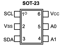
[SDA | p[3] ]
[SCL | p[1] ]
[VCC | p[6] ]
[VSS | p[2] ]
[A0 | p[5] ]
[A1 | p[4] ]
This table is an example from the Microchip, 24AA025 EEPROM chip.
In this particular example - there is a 1:1 mapping between the schematic symbol pins and the pads of the landpattern. Both the pin and the pads are of type Ref. For the pin properties, this means that each name SDA, SCL, etc are defined as SinglePin ports on this component. For the pads, we are referencing the conventional p array that defines the pins of a landpattern. This means that p[1] corresponds with pin 1, p[2] corresponds with pin 2, etc:
This table could have been defined identically as:
pcb-component EEPROM-24AA025:
  ...

  pin-properties :
    [pin:Ref | pads:Int ... ]
    [SDA     | 3            ]
    [SCL     | 1            ]
    [VCC     | 6            ]
    [VSS     | 2            ]
    [A0      | 5            ]
    [A1      | 4            ]
Notice that in this case pads is of type Int and we don't use the p[*] syntax. We reference the integer pin directly. This is a short hand for the p[*] syntax.
For this simple example - it may not be obvious why you might use a Ref instead of a Int. Typically, we see Ref used for large BGA packages where you will see K[1], N[5], AB[2], or similar references from a 2D grid.
N:1 Pads to Ports
There are some cases where you may want to assign multiple land pattern pads to a single port. This is very common for ground and power pins in large packages.
pcb-component FPGA:
  ...

  pin-properties :
    [pin:Ref | pads:Ref ... ]
    [ VCCINT  | A[2] B[10] C[3] C[4]  ]
    [ GND     | A[3] A[7] B[2] B[8]  ]
    ...
In this example, we construct a component with multiple pads devoted to the VCCINT and GND pins.
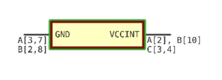
Notice how each of the pins has multiple pads associated with it. The engine attempts to shorten the pad references shown next to the pin as much as it can. In this case, it means that for each C pad referenced in VCCINT, we use a , (comma) delimited list of indices. Similarly in GND, both the A and B pads have 2 indices listed.
This style of N:1 pad to pin referencing can be useful but if the value of N grows large, this can become unwieldy. Another way to structure this would be to use unique pins for each pad (ie, strictly 1:1 mapping):
pcb-component FPGA:
  ...

  pin-properties :
    [pin:Ref | pads:Ref ... ]
    [ VCCINT[0] | A[2]  ]
    [ VCCINT[1] | B[10] ]
    [ VCCINT[2] | C[3]  ]
    [ VCCINT[3] | C[4]  ]

    [GND[0]     | A[3] ]
    [GND[1]     | A[7] ]
    [GND[2]     | B[2] ]
    [GND[3]     | B[8] ]

    ...
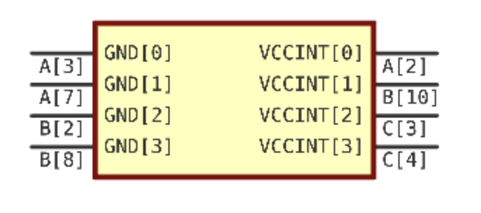
In this variant, each of the VCCINT and GND pins has a 1:1 mapping with a pad. This can be useful for the case where there may be 10's or 100's of these pins. This trades more schematic pixel space for a more readable pin to pad mapping.
Individually listing each pins in a table like this is going to become a bit tedious though. Fortunately, we're not just entering data, we can write a bit of code too:
  val VCCINT-PADS = [
    Ref("A")[2],
    Ref("B")[10],
    Ref("C")[3],
    Ref("C")[4]
  ]

  pin-properties :
    [pin:Ref | pads:Ref ... ]
    for (rf in VCCINT-PADS, i in 0 to false) do:
      [ VCCINT[i] | (rf) ]
The VCCINT-PADS tuple in this example is a bit contrived. The more likely source of the pad information for a component would be a file like the Xilinx Pinout Package files. The important part is the use of the for loop to construct each of the rows of the pin-properties table.
Note the use of the () around the rf value. These parenthesis are necessary to convert the value into a Ref symbol.
Assigning Properties for the Box Symbol
The pin and pads properties are not the only features that we can add through the pin-properties table.
The header of the table is customizable and allows any number of properties to be assigned to each pin
as needed.
Here is an example where we assign a side property of type Dir to each pin. These types of properties
are very useful for when working with the "BoxSymbol" utilities:
pcb-component mycomponent :
  mpn = "DAC53001"
  pin-properties :
    [pin:Ref | pads:Int ...        | side:Dir   ]
    [VDD     | 15                  | Right ]
    [VREF    | 16                  | Right ]
    [OUT0    | 2                   | Right ]
    [FB0     | 1                   | Right ]
    [CAP     | 13                  | Right ]
    [SDO     | 5                   | Left ]
    [SYNC#   | 6                   | Left ]
    [SDI     | 7                   | Left ]
    [SCLK    | 8                   | Left ]
    [NC      | 3, 4, 9, 10, 11, 12 | Left ]
    [AGND    | 14, 17              | Left  ]

  val box = BoxSymbol(self)

  set-alignment(N, self.VDD, self.VREF)
  set-alignment(S, self.AGND, self.NC, self.CAP)

  set-head-margin(1.0, self.NC)
  set-head-margin(1.0, self.OUT0, self.FB0)

  val symb = create-symbol(box)
  assign-symbol(symb)
Here is an example rendering of this component:
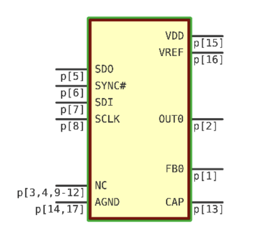
Notice how the pins of the symbol get assigned to one side or the other depending on
the side property. Notice also that the order of the pins in the box symbol depends on
the ordering in the table. Some of the details regarding the formatting are left out in this
example.
Another point of interest is that the NC and AGND are multi-pad pins in this symbol. Notice
how for those pins, the pad identifier for the pin has multiple pad references in it.
This symbol was created with the BoxSymbol from JSL. See JSL for more information about how to set alignment, margin, and other properties.
Assigning the Bank via the Table
The bank property is used to construct multi-part symbols. We can assign the bank association in the pin-properties table. The bank property is of type Int|Ref meaning that it can either be
an Int value or a Ref value. When building a part, you will typically use all Int or all Ref for the banks
in a component.
Here is an excerpt of a component that uses the bank property as a Ref in the pin properties table:
public pcb-component USBMux :
  manufacturer = "Texas Instruments"
  mpn = "HD3SS3220RNHR"
  reference-prefix = "U"

  port TX-O : diff-pair
  port RX-O : diff-pair

  port TX : diff-pair[[1, 2]]
  port RX : diff-pair[[1, 2]]

  pin-properties :
    [pin:Ref | pads:Ref ... | side:Dir | bank:Ref]
    [VBUS_DET     | p[5]  | Left  | control]
    [ID           | p[27] | Left  | control]
    [CC2          | p[1]  | Left  | control]
    [CC1          | p[2]  | Left  | control]
    [CURRENT_MODE | p[3]  | Left  | control]
    [PORT         | p[4]  | Left  | control]
    [ENn_CC       | p[29] | Left  | control]
    [TX-O.P       | p[6]  | Right | mux]
    [TX-O.N       | p[7]  | Right | mux]
    [RX-O.P       | p[9]  | Right | mux]
    [RX-O.N       | p[10] | Right | mux]
    ...
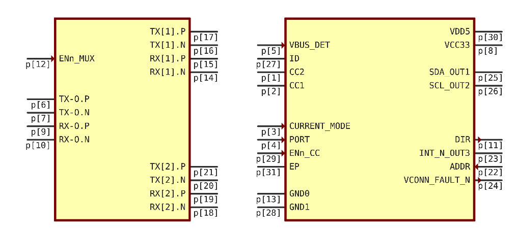
This results in two symbol parts for the component:
Multiple Pin Property Tables
When defining pin-properties tables, the number of rows typically equals the number of pins in the component we are attempting to model. With a large number of pins, this amount of data can be quickly become overwhelming. Adding or removing columns from the table becomes a chore.
Because of this it is common to keep the tables focused on one particular application at a time. For example, the primary application is creating the pin to pad mapping. That is what the first (and usually only) pin-properties table will do.
Once you have defined this mapping, you can either add columns to this table to introduce other properties, or you create an entirely new table. If we refer back to the 24AA025 example from earlier, we could add a second table in our component definition like this:
pcb-component EEPROM-24AA025:
  ...

  pin-properties :
    [pin:Ref | pads:Int ... ]
    [SDA     | 3            ]
    [SCL     | 1            ]
    [VCC     | 6            ]
    [VSS     | 2            ]
    [A0      | 5            ]
    [A1      | 4            ]

  pin-properties:
    [pin:Ref | side:Dir ]
    [SDA     | Left  ]
    [SCL     | Left  ]
    [VCC     | Right ]
    [VSS     | Left  ]
    [A0      | Right ]
    [A1      | Right ]

  ...
This example is a trivial case, but you could imagine adding additional custom properties or other data.
The important things to consider are:
- The
pin:Refcolumn is like the "Primary Key" of this table. Everypin-propertiestable instance will need to reference thepin:Refproperty as the first column. - The first
pin-propertiestable defines the ports of the component. Thepin:Refproperties in subsequent tables must match with thepin:Refproperties in the first table.- The subsequent tables can have a sub-set of the
pin:Refproperties from the first table. - No new, unique
pin:Refproperties can be defined in subsequent tables.
- The subsequent tables can have a sub-set of the
For example - This is OK:
  pin-properties :
    [pin:Ref | pads:Int ... ]
    [SDA     | 3            ]
    [SCL     | 1            ]
    [VCC     | 6            ]
    [VSS     | 2            ]
    [A0      | 5            ]
    [A1      | 4            ]

  ; OK - properties only defined on these pins.
  pin-properties:
    [pin:Ref | card:Cardinality ]
    [SDA     | Bidir  ]
    [SCL     | Bidir  ]
    [A0      | Input ]
    [A1      | Input ]
We don't define any new pins - we just don't include the VCC and VSS in the second table. This means that SDA, SCL, A0, and A1 will all have a card property but VCC and VSS will not.
But the following is NOT OK:
  pin-properties :
    [pin:Ref | pads:Int ... ]
    [SDA     | 3            ]
    [SCL     | 1            ]
    [VCC     | 6            ]
    [VSS     | 2            ]
    [A0      | 5            ]
    [A1      | 4            ]

  ; BAD - Will throw an error
  pin-properties:
    [pin:Ref | pads:Int ... ]
    [NC      | 7  ]
    [NC      | 8  ]
This will result in the runtime throwing an exception.
Ignored Values on Properties
Sometimes you have a table structure and you don't want to set a property on a particular pin. The - special value is here to the rescue. This value basically means "Don't set this property".
  pin-properties :
    [pin:Ref | pads:Int ... ]
    [SDA     | 3            ]
    [SCL     | 1            ]
    [VCC     | 6            ]
    [VSS     | 2            ]
    [A0      | 5            ]
    [A1      | 4            ]

  ; OK - properties only defined on these pins.
  pin-properties:
    [pin:Ref | card:Cardinality | i2c-bus:(True|False) ]
    [SDA     | Bidir  | true ]
    [SCL     | Bidir  | true ]
    [A0      | Input  | -    ]
    [A1      | Input  | -    ]
Notes:
- Notice that in the
i2c-bus:(True|False)property type, there is a set of()around theTrue|Falsetype. This is necessary for all Union Types inpin-propertiesheaders. Otherwise, you will get a syntax error. - The
-special value basically means thatA0andA1in this example will not have ai2c-busproperty. Thehas-property?(self.A0.i2c-bus)function will returnfalse.