Land Patterns
A pcb-landpattern statement defines the pads and associated geometry for the interface between an electrical component and the PCB. This is also known as a footprint, package, or land-pattern.
Signature
pcb-landpattern lp-name (arg1:Type1, ...) :
  name = <String|False>
  description = <String|False>

  external-names = <Tuple<String>|False>
  model3d = <Model3D>

  <PAD-1>
  ...
  <LAYER-1>
  ...
The expression name lp-name uniquely identifies this package definition
in the current context.
The argument list (arg1:Type1, ...) is optional and provides a means of
constructing parameterized landpattern definitions.
name- This name is used in the UI as a more user friendly name. If this string is not provided then thelp-nameexpression is used as the landpattern's name.description- This string is defining more meta-data for the landpattern.external-names- Optional tuple ofStringinstances of alternate names for this landpattern.model3d- The model3d statement expects aModel3Dinstance to define the data and pose for the 3D model of this component.<PAD-1>- A pad statement defines a electrical connection interface point.- The landpattern expects zero or more pads.
- The pad reference is part of the
pcb-symbol -> pcb-landpatternmapping in the pcb-component definition. <LAYER-1>- A layer() statement defines what geometry to create on the non-copper layers.
Usage
Here is a typical land-pattern example, featuring a 3-pin SOT-23 :
pcb-landpattern Static-SOT23 :

  val x0 = 1.0  ; Lead-Span spacing
  val y0 = 0.95 ; Pitch
  ; Pad Definitions
  val pdef = smd-pad(0.8, 0.5)
  pad p[1] : pdef at loc((- x0), y0)
  pad p[2] : pdef at loc((- x0), (- y0))
  pad p[3] : pdef at loc(x0, 0.0)

  ; Non-Copper Geometry
  layer(Courtyard(Top)) = Rectangle(3.3, 3.0)
  layer(Silkscreen("f-silk", Top)) = LineRectangle(3.3, 3.0)
  ; Reference Designator Helper Function
  ref-label()
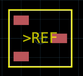
If we attempt to visualize this landpattern:
view(Static-SOT23)
In this definition, notice that you can use standard stanza syntax like defining immutable values (eg, val x0 = -0.95). This can make constructing landpatterns easier because we can use arithmetic directly in the land-pattern definition.
What the >REF?
The
>REFtext in the silkscreen might be a bit jarring at first, but keep in mind that we are defining the land pattern - this isn't what is going to be in the resultant board. The>REFwill get replaced by a reference designator and that designator will be positioned automatically.
Pad Definitions
The definition for smd-pad can be found in OCDB. This defines a typical surface mount pad. There are multiple ways of invoking smd-pad:
; Originating Definitions
pcb-pad smd-pad (copper-layer:Shape, solder-mask-layer:Shape|False, paste-layer:Shape) :
  ...

; Polymorphic Functions
defn smd-pad (s:Shape) -> Pad
defn smd-pad (anchor:Anchor, width:Double, height:Double) -> Pad
defn smd-pad (d:Dims) -> Pad
defn smd-pad (width:Double, height:Double) -> Pad
The top definition is the base pcb-pad definition and then the following functions are all different ways to create that originating definition. These are polymorphic functions.
Poly-Wut? - Polymorphism is a fancy way of saying that the compiler is going take whatever args you give for a particular function and do its level best to call the right function to give you the result you want. It may not be able to satisfy every request. This may be due to a lack of a definition that supports that modality. Or it may be due to an ambiguity in the definition or the invocation.
Big Picture - The
smd-padsymbol encodes the core idea - eg, This function returns a surface mount pad definition. All of the polymorphic versions of this function must adhere to that core idea.
Layer Content
The next section of the pcb-landpattern definition is the non-copper layer() statements. This includes the courtyard, silkscreen, forbid/keepout regions, and any other pertinent content you might wish to include in the land-pattern.
The ref-label function is a generator. Here is an excerpt from the ref-label definitions:
defn ref-label (pose:Pose, anchor:Anchor) :
  inside pcb-landpattern:
    val min-height = clearance(current-rules(), MinSilkscreenTextHeight)
    layer(Silkscreen("values", Top)) = Text(">REF", min-height, anchor, pose)

defn ref-label () :
  ref-label(loc(0.0, 0.0), C)
The inside pcb-landpattern statement is what makes this function a generator. The lines inside this statement effectively get copied in to the parent context (in this case, the Static-SOT23 land-pattern definition).
The idea is that inserting a reference designator label into a pcb-landpattern definition is a pretty common activity. Copying and pasting this into every pcb-landpattern definition would get annoying fast. It also would be pretty significant violation of the "Don't Repeat Yourself" principle. The ref-label generator allows us to inject content into the parent context without necessarily knowing when and where it will get used.
Arguments to a Land Pattern
Arguments to a landpattern can be an effective way to construct highly reusable land patterns:
pcb-landpattern header (num-pins:Int, pitch:Double = 2.54):
  val pdef = pth-pad(0.9, 1.15)
  for i in 1 through num-pins do:
    pad p[i] : pdef at loc(to-double(i  - 1) * pitch, 0.0)
  ...
These arguments allow us to construct an N-pin through-hole single-row header and customize its pitch. The pitch argument has a default value making it optional.
You can find a more advanced example of pcb-landpattern with arguments here.
Statements
Here is the list of all of the statements you can use in a pcb-landpattern :
| Statement | Description |
|---|---|
description |
Description for the land pattern |
external-names |
Define common names for the land pattern |
layers |
Define shapes on layers like SolderMask |
name |
Name of the land pattern |
pad |
Creates pads you can connect to |
model3d |
Associate a 3D model with a landpattern |
copper |
Construct unassociated copper geometry in the landpattern |
via |
Construct unassociated via placements in the landpattern |