Model a power regulator
This tutorial walks you through creating a simple parametric regulator using the AP2205 adjustable LDO from Diodes Incorporated, and adding it as a component library. We'll walk through creating a new project, adding a new component to an existing library, modelling the main IC, and then follow up with a parametric module to solve for any desired output voltage.
Contents
- Model a power regulator
Setting up the code
Create a new project
First, create a new project
Create a new component
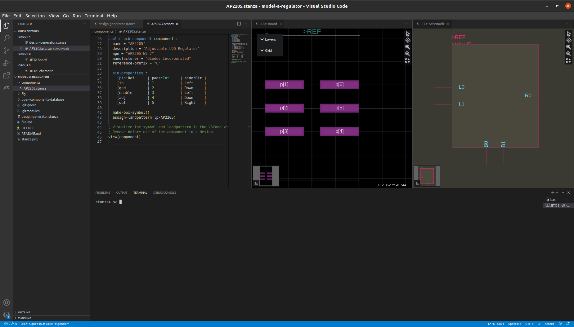
Next, click on the JITX pane and select "Create component." Make a new folder named components and choose it as the parent directory. Name the component file AP2205. This will create a file called <your-component-name>.stanza, but you should type in only the component name (not the .stanza file extension).
Add the components library to stanza.proj
Copy-paste this line into the stanza.proj file to import all the component files in /components/ into our project.
packages components/* defined-in "components" ; notice the extra s
Modeling the Component
Update the Pin Properties
Initially our component definition looks like this :
public pcb-component component :
  name = "AP2205"
  description = "PART, DESCRIPTION, DETAILED"
  mpn = "MANUFACTURER PART NUMBER"
  manufacturer = "MANUFACTURER NAME"
  reference-prefix = "LETTER"

  pin-properties :
    [pin:Ref      | pads:Int ... | side:Dir ]
    [VCC          | 1            | Up       ]
    [GND          | 6            | Down     ]
    [PINNAME1     | 2            | Left     ]
    [PINNAME2     | 3            | Right    ]
    [PINNAME3     | 4            | Left     ]
    [PINNAME4     | 5            | Right    ]

  make-box-symbol()
  assign-landpattern(lp-AP2205)

  supports power:
    power.vdd => self.VCC
    power.gnd => self.GND
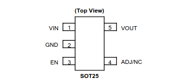
We need to update this with the information from the datasheet.
public pcb-component component :
  name = "AP2205"
  description = "Adjustable LDO Regulator"
  mpn = "AP2205-W5-7"
  manufacturer = "Diodes Incorporated"
  reference-prefix = "U"

  pin-properties :
    [pin:Ref      | pads:Int ... | side:Dir ]
    [vin          | 1            | Left     ]
    [gnd          | 2            | Down     ]
    [enable       | 3            | Left     ]
    [adj          | 4            | Down     ]
    [vout         | 5            | Right    ]

  make-box-symbol()
  assign-landpattern(lp-AP2205)
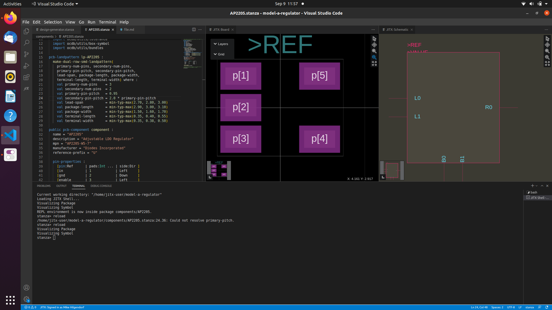
Reload the design to view the changes. You'll notice that the schematic symbol is updated.
We've also removed the supports power statement - we won't need it in this example.
Finally we add some electrical properties that enable automatic design and checking.
public pcb-component component :
  name = "AP2205"
  description = "Adjustable LDO Regulator"
  mpn = "AP2205-W5-7"
  manufacturer = "Diodes Incorporated"
  reference-prefix = "U"

  pin-properties :
    [pin:Ref      | pads:Int ... | side:Dir ]
    [vin          | 1            | Left     ]
    [gnd          | 2            | Down     ]
    [enable       | 3            | Left     ]
    [adj          | 4            | Down     ]
    [vout         | 5            | Right    ]

  make-box-symbol()
  assign-landpattern(lp-AP2205)

  val gen-props = ocdb/utils/property-structs/GenericPin(min-max(0.0, 36.0), 1000.0)
  property(self.vin.generic-pin) = gen-props
  property(self.enable.generic-pin) = gen-props
  property(self.vin.generic-pin) = gen-props
  property(self.vin.power-pin) = ocdb/utils/property-structs/PowerPin(min-max(2.3, 24.0))
  property(self.adj.vref) = 1.24
  property(self.vout.max-current) = 250.0e-3
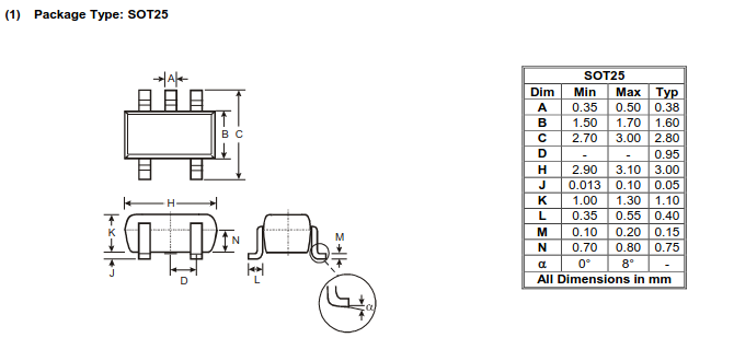
Model the Landpattern
We need to model the SOT-25 landpattern required by this part. By default the component creation tool makes an SOIC landpattern with the call to make-n-pin-soic-landpattern. We'll replace this with another generator from ocdb/utils/landpatterns called make-dual-row-smd-landpattern which creates two rows of pads with different pitches and numbers of pins.
Don't copy paste this. This code block is already built in to JITX.
public defn make-dual-row-smd-landpattern (
  primary-num-pins:    Int,     ; number of pins on one side of the land pattern
  secondary-num-pins:  Int,     ; number of pins on the other side of the land pattern
  primary-pin-pitch:   Double,  ; the pitch of pins on the primary side of the land pattern
  secondary-pin-pitch: Double,  ; the pitch of the pins on the other side of the land pattern
  lead-span:       Toleranced,  ; the lead span across the land pattern
  package-length:  Toleranced,  ; the length of the package
  package-width:   Toleranced,  ; the width of the package
  terminal-length: Toleranced,  ; the length of the terminals
  terminal-width:  Toleranced) : ; the width of the terminals
To do this we remove the body of lp-AP2205 first :
pcb-landpattern lp-AP2205 :
And add a call to make-dual-row-smd-landpattern
pcb-landpattern lp-AP2205 :
  make-dual-row-smd-landpattern(
    primary-num-pins, secondary-num-pins,
    primary-pin-pitch, secondary-pin-pitch,
    lead-span, package-length, package-width,
    terminal-length, terminal-width)
We don't have values for each of these fields yet, so let's add a where : clause and fill them in.
pcb-landpattern lp-AP2205 :
  make-dual-row-smd-landpattern(
    primary-num-pins, secondary-num-pins,
    primary-pin-pitch, secondary-pin-pitch,
    lead-span, package-length, package-width,
    terminal-length, terminal-width) where :
    val primary-num-pins    =
    val secondary-num-pins  =
    val primary-pin-pitch   =
    val secondary-pin-pitch =
    val lead-span           =
    val package-length      =
    val package-width       =
    val terminal-length     =
    val terminal-width      =
We grab the actual values from the data sheet :
pcb-landpattern lp-AP2205 :
  make-dual-row-smd-landpattern(
    primary-num-pins, secondary-num-pins,
    primary-pin-pitch, secondary-pin-pitch,
    lead-span, package-length, package-width,
    terminal-length, terminal-width) where :
    val primary-num-pins    = 3
    val secondary-num-pins  = 2
    val primary-pin-pitch   = 0.95                          ; D
    val secondary-pin-pitch = 2.0 * primary-pin-pitch
    val lead-span           = min-typ-max(2.70, 2.80, 3.00) ; C
    val package-length      = min-typ-max(2.90, 3.00, 3.10) ; H
    val package-width       = min-typ-max(1.50, 1.60, 1.70) ; B
    val terminal-length     = min-typ-max(0.35, 0.40, 0.55) ; L
    val terminal-width      = min-typ-max(0.35, 0.38, 0.50) ; A
Reloading the component will show the component with its correct landpattern.
Create a Solver
The adjustable LDO is only useful if we can place it in a circuit. Instead of forcing users of the library to compute their resistor values each time they use the LDO, we can write a module generator that will solve for the resistor values for a desired output voltage.
Define the pcb-module
First we'll define a new module that takes vout as an argument.
public pcb-module module (vout:Double) :
Now let's define the input/output ports. We will have two ports for voltage, in and out that can be net to other power ports in the design, and an enable pin for the LDO.
; inside pcb-module
  port in  : power
  port out : power
  pin enable
Now we can add the LDO and wire power and ground nets. We also add input and output capacitors to the ldo.
  ; Instantiate the component
  inst ldo : components/AP2205/component

  ; Wire up the LDO to the module ports
  net VIN  (ldo.vin,  in.vdd)
  net VOUT (ldo.vout, out.vdd)
  net GND  (ldo.gnd, in.gnd, out.gnd)
  net (ldo.enable, enable)

  cap-strap(ldo.vin,  ldo.gnd, 1.0e-6)
  cap-strap(ldo.vout, ldo.gnd, 2.2e-6)
In order to make our call to cap-strap work, we need to import the generic components. Paste the below line with the other import statements.
import ocdb/utils/generic-components
Finally we use the voltage-divider solver to design the feedback network for us and then we connect it up.
  inst output-voltage-divider : ocdb/modules/passive-circuits/voltage-divider(source-voltage = high-voltage, divider-output = adj-voltage, tolerance = tolerance, current = current) where :
    val high-voltage = vout
    val adj-voltage = property(ldo.adj.vref) as Double
    val tolerance = 1.0
    val current = 0.5e-3

  net (output-voltage-divider.in, ldo.vout)
  net (output-voltage-divider.out, ldo.adj)
  net (output-voltage-divider.lo, ldo.gnd)
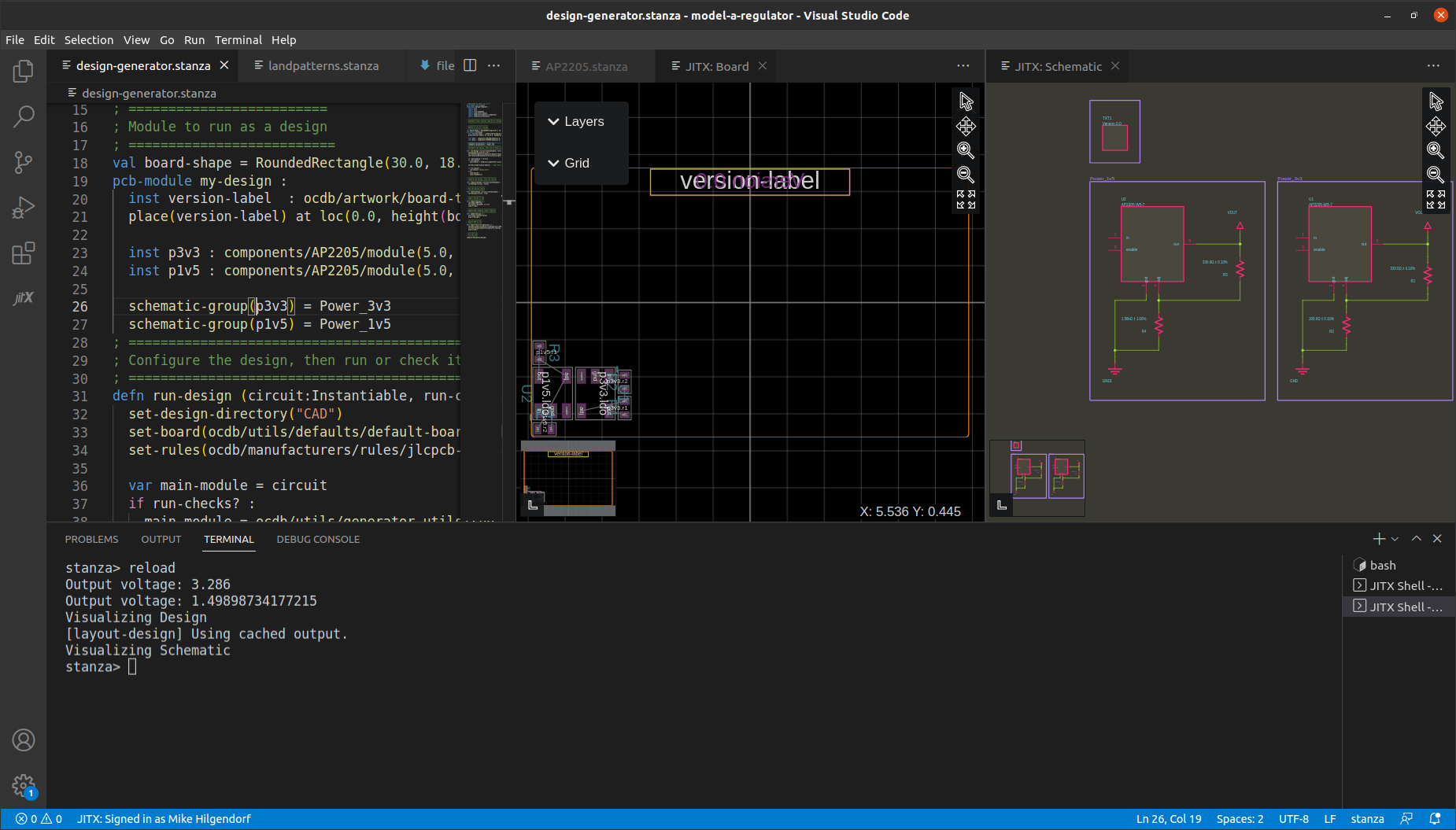
Add to the main.stanza design generator
In your project's main.stanza you can now instantiate the component module
pcb-module my-design :
  inst version-label  : ocdb/artwork/board-text/version-silkscreen("Version 0.0")
  place(version-label) at loc(0.0, height(board-shape) / 2.0 - 1.0) on Bottom

  inst p3v3 : components/AP2205/module(3.3)
  inst p1v5 : components/AP2205/module(1.5)

  net GND (p3v3.in.gnd p1v5.in.gnd)
  symbol(GND) = ocdb/utils/symbols/ground-sym

  schematic-group(p3v3) = Power_3v3
  schematic-group(p1v5) = Power_1v5
Adding Electrical Properties for checks
JITX includes advanced mechanisms for checking the electrical properties of a design, but these checks typically involve adding some property values to components and nets.
First we need to update the defpackage statement to include some helper structs from ocdb :
#use-added-syntax(jitx)
defpackage components/AP2205:
  import core
  import collections
  import jitx
  import jitx/commands
  import ocdb/utils/defaults
  import ocdb/utils/landpatterns
  import ocdb/utils/box-symbol
  import ocdb/utils/bundles
  import ocdb/utils/generic-components
  import ocdb/utils/property-structs ; <--- helpers for checks
See the code for the complete design
We'll be using the following :
GenericPin: Generic pin properties (absolute maximum ratings for voltage and ESD)PowerPin: Properties for power pins (recommended input voltage range)PowerSupplyPin: Properties for pins that supply power (voltage range, maximum current)
We can get the values we need from the absolute maximum ratings table in the datasheet, compute the values we need, and add to the pin-properties table.
public pcb-component component :
  name = "AP2205"
  description = "Adjustable LDO Regulator"
  mpn = "AP2205-W5-7"
  manufacturer = "Diodes Incorporated"
  reference-prefix = "U"

  ; Compute the power and generic pin properties
  val recommended-voltage = min-max(2.3, 24.0)
  val maximum-voltage     = typ(36.0)
  val esd-voltage         = 1000.0

  val power-props = PowerPin(recommended-voltage)
  val gen-props   = GenericPin(maximum-voltage, esd-voltage)
  val max-output-current = 250.0e-3

  pin-properties :
    [pin:Ref      | pads:Int ... | side:Dir | generic-pin:GenericPin | power-pin:PowerPin | max-current:Double ]
    [in           | 1            | Left     | gen-props              | power-props        | -                  ]
    [gnd          | 2            | Down     | gen-props              | -                  | -                  ]
    [enable       | 3            | Left     | gen-props              | -                  | -                  ]
    [adj          | 4            | Down     | gen-props              | -                  | -                  ]
    [out          | 5            | Right    | gen-props              | -                  | max-output-current ]
Note: since we are using an adjustable LDO, we don't know what the output voltage of the component is, and can't assign a
PowerSupplyPinto its pin properties yet!
Now we need to update the module to assign the power supply pin property to the LDO, and a net voltage property on the output, at the very end of the module.
  ; Assign the property to the LDO's output pin. We lookup the
  ; maximum current using the `property(...)` introspection.
  property(ldo.out.power-supply-pin) =
    PowerSupplyPin(output-voltage, property(ldo.out.max-current))
Final Notes
There is more detail we could add to this model to catch the details like maximum pin voltage and current, which are not captured by a simple netlist. Later tutorials will show you how to capture details that will validate this circuit automatically, so we will have confidence that our design will work.