LayerSpecifier
The LayerSpecifier type is the base type for identifying non-copper manufacturing layers. This typically includes the silkscreen, solder mask, forbidden regions, etc. It does not include the copper layers. To identify copper layers, we use the LayerIndex type.
Derived Types
LayerSpecifier is the parent to multiple child types. The child types defined below are what we typically use with the layer() statement.
| Name | Description |
|---|---|
Courtyard(s:Side) | Courtyard layer to indicate land pattern bounds. Expects a Top|Bottom argument. |
Cutout() | Cutout layer for holes and slots. Vias and through-hole pads will include their hole definitions on this layer. |
SolderMask(s:Side) | Solder mask layer. Expects a Top|Bottom argument. |
Paste(s:Side) | Paste application layer. Expects a Top|Bottom argument. |
Glue(s:Side) | Glue application layer. Expects a Top|Bottom argument. |
Finish(s:Side) | Surface Finish layer to indicate plating. Expects a Top|Bottom argument. |
Silkscreen(<br>  name:String,<br>  s:Side<br>) | Silkscreen application layer. Expects a string name and a Top|Bottom argument. |
BoardEdge() | Geometry to align with edge of board |
ForbidVia() | Forbid Vias layer (via keepout) |
ForbidCopper(<br>  start:LayerIndex,<br>  end:LayerIndex<br>) | Forbid Copper layer (copper keepout). Expects a LayerIndex argument to specify which layer[s] to forbid copper. |
CustomLayer(<br>  name:String,<br>  s:Side<br>) | Custom Mechanical layer. Expects a name and a Top|Bottom argument. |
Cutout
The Cutout layer is intended to make internal holes in the board shape, like for through holes or routed holes/slots.
While you can use any geometry on the Cutout layer - keep in mind your fabricator's limitations and constraints. If your fabricator only has a router (and not a laser or waterjet cutter) then they will likely not be able to construct a hole with squared corners.
Silkscreen
This layer expects a name:String argument. This name acts like a class attribute in HTML. It is intended to group like content together.
When the board data is exported, the silkscreen content for the top and bottom layers, respectively, will be flattened into a single top and bottom silkscreen layer.
CustomLayer
Similarly, the CustomLayer specifier expects a name:String argument. This argument allows the user to specify different classes of content like:
- Fabrication Notes
- Assembly Notes
- Dimensions
See the following links for how these layers map to export backends:
ForbidCopper
The ForbidCopper specifier takes a LayerIndex instance[s] as an argument. This allows you to construct keepout regions for the copper on any layer or set of layers in a design.
defn ForbidCopper (start:LayerIndex, end:LayerIndex = start) -> ForbidCopper :
  ...
Notice that the end by default is start. If you construct a ForbidCopper() with a single argument, then only that copper layer will possess a forbidden region.
Let's consider a case where we have an antenna on a N-layer board:
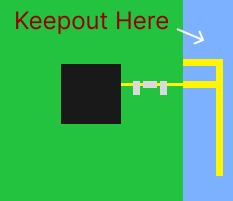
And we want to place a forbid region in the blue area of the board.
pcb-board curr-board:
  ...
  val forbid-range = ForbidCopper(
    LayerIndex(1), LayerIndex(0, Bottom)
  )
  layer(forbid-range) = loc(40.0, 0.0) * Rectangle(10.0, 30.0)
Here we construct a ForbidCopper instance that spans the layer 1 to N. Notice that we don't include the layer 0 or the Top layer because that is where the antenna structure will go. The LayerIndex(0, Bottom) is a means of specifying the bottom copper layer of the board without knowing the full number of layers in the stackup.
We then use the loc() function to position the desired forbid region on the board. This takes our 10mm x 30mm forbid region and translates it 40mm to right from the origin of the board.