Revising an Existing Altium Design in JITX
This tutorial will walk through importing an existing design from Altium to JITX, modifying the design, exporting the design from JITX to Altium, and updating the layout.
You'll need:
- A licenced copy of Altium with the JITX extension installed
- An Altium project
Follow the steps in Install Altium JITX Extension before starting this.
This tutorial uses the Altium files for the STM32 Nucleo-64 development board - external link.
Sections:
- Import the Altium Project to JITX
- Make changes to the project
- Export the JITX Project to Altium
- Update the layout
- Rapid changes we can make in JITX
- Summary
Import the Altium Project to JITX
Follow the workflow outlined in Importing Altium to JITX to bring your project into JITX.
Make changes to the project
This project has several passive components that are out of stock and that we would like to replace with smaller components for a more integrated layout. It also has a series of jumpers, which we won't want in a more integrated project. There's a land pattern with silkscreen around one of the solder balls that will cause a manufacturing stoppage. We'll update the passive components for optimized checking, selection and sourcing. Remove connected jumpers and tie nets directly. And update the BGA land pattern.
These are some typical steps we may take when importing reference designs and using it in a different application.
We will make the following changes:
- Change the capacitors to generic, in-stock components
- Change the resistors to generic, in-stock components
- Remove jumpers and tie nets directly
- Update BGA land pattern
We will also open the generated file by pressing Ctrl+p and typing mb1367.stanza or double clicking on the file in the explorer window.
Open mb1367.stanza in VSCode, then go to File then Save As... and save it as motorcontroller.stanza. We'll make edits to this new file. Having the original file will be useful in case we want to do a file compare on our changes later.
We'll visualize the imported design by opening the output folder in VSCode and running from the VSCode terminal:
jitx repl motorcontroller.stanza
We can then rearrange our windows to see the generated code, the schematic, and the layout.
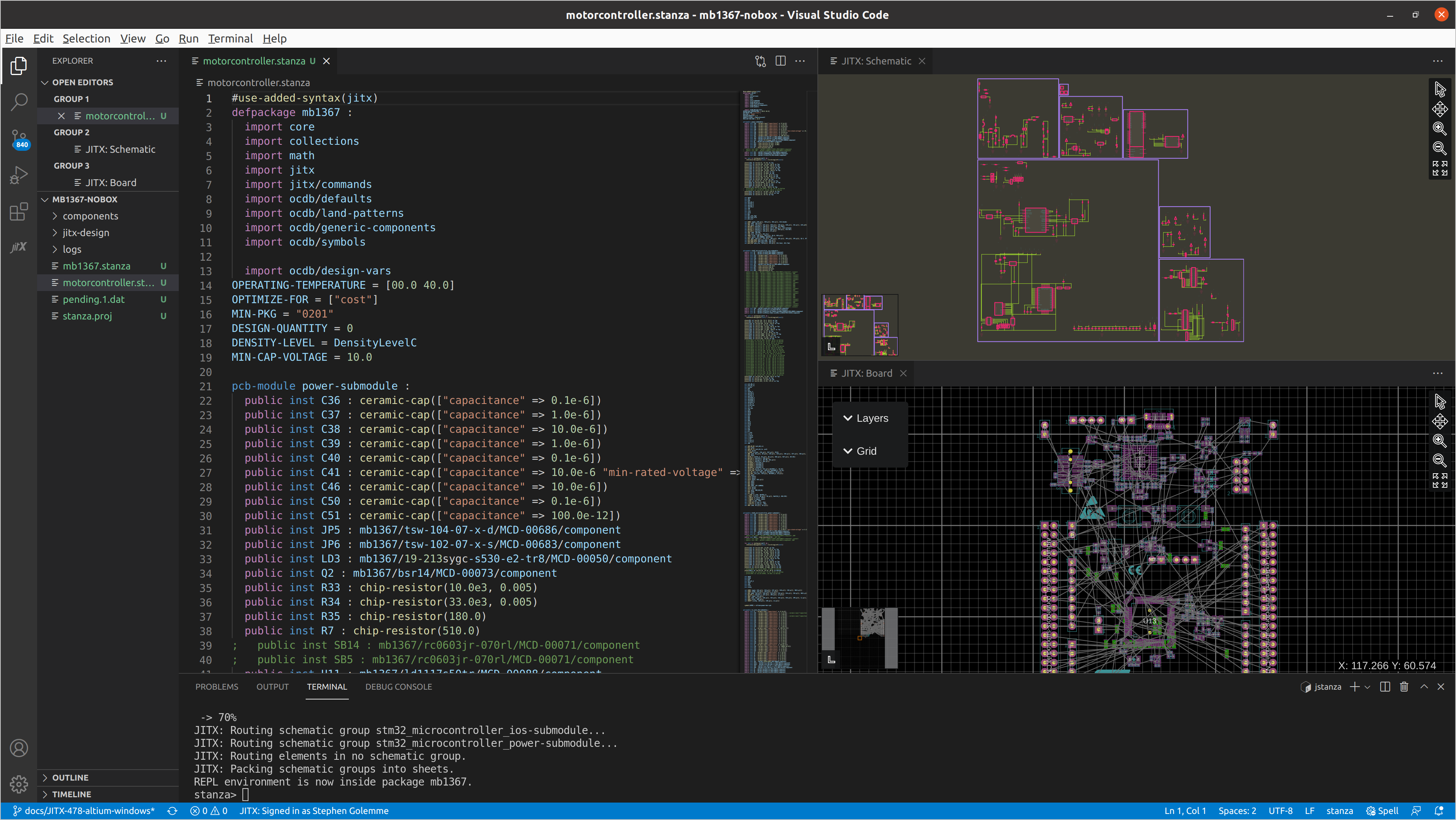
As we make changes, we can periodically test our code by saving
motorcontroller.stanzaand typingreloadat the stanza prompt.
We can see each schematic page is represented as a distinct box in the schematic viewer and in the stanza file as a schematic group. They are broken up into individual modules and called in the main pcb-module:
schematic-group(arduino_extension_connectors-submodule) = arduino_extension_connectors-submodule
schematic-group(mechanical-submodule) = mechanical-submodule
schematic-group(power-submodule) = power-submodule
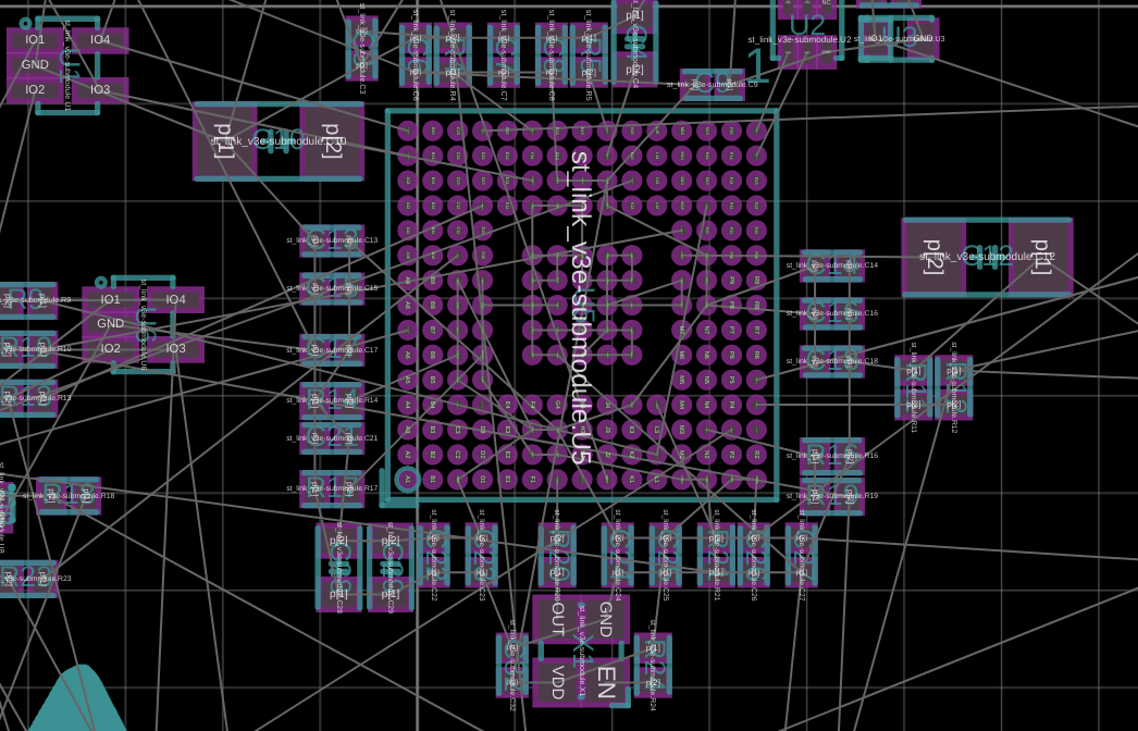
schematic-group(st_link_v3e-submodule) = st_link_v3e-submodule
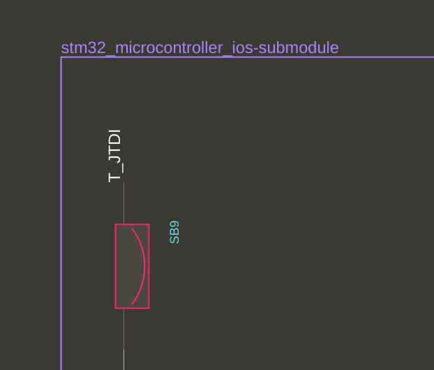
schematic-group(stm32_microcontroller_ios-submodule) = stm32_microcontroller_ios-submodule
schematic-group(stm32_microcontroller_power-submodule) = stm32_microcontroller_power-submodule
We can see the land patterns of each component in its location on the board.
The import tool did not bring in the routing, because we don't need it yet. Later we'll bring the routing back in, and merge changes in a way that preserves traces and copper pours.
At the top of the file after our imports, we start with the power-submodule, which has 5 sections. The power-submodule corresponds to the schematic page titled Main power 5V / 3V3.
- Components are instantiated.
public inst ...The public statement means the component can be accessed outside of thepcb-module:
pcb-module power-submodule :
  public inst C36 : mb1367/cc0402krx7r7bb104/MCD-00102/component
  public inst C37 : mb1367/cc0603krx5r7bb105/MCD-00010/component
  public inst C38 : mb1367/cc0805krx5r8bb106/MCD-00014/component
  public inst C39 : mb1367/cc0603krx5r7bb105/MCD-00010/component
  ; ...
  public inst SB5 : mb1367/rc0603jr-070rl/MCD-00071/component
  public inst U11 : mb1367/ld1117s50tr/MCD-00088/component
  public inst U12 : mb1367/ld39050pu33r/MCD-00215/component
  public inst U14 : mb1367/tl1431cl5t/MCD-01802/component
- For each instance name, the component is assigned the reference designator name:
  for inst in instances(self) do :
    reference-designator(inst) = to-string(ref(inst))
- Component instances are placed at specific X, Y and rotations on either the
ToporBottomof the board.
  place(C36) at loc(33.57, 47.24) on Top
  place(C37) at loc(30.245, 45.615, 90.0) on Top
  place(C38) at loc(17.47, 44.515, 270.0) on Top
  place(C39) at loc(35.195, 44.365, 270.0) on Top
- Nets that connect the submodule to the rest of the board are exposed with
pin name:
  pin p3v3
  pin p5v
  pin p5v_usb_chgr
  pin p5v_usb_stlk
  pin p5v_vin
- The internal netting is established:
  net AGND (agnd, C46.p[1], C50.p[1], R34.p[1], U14.Anode)
  net E5V (e5v, JP5.p[5])
  net GND (gnd, C36.p[1], C37.p[1], C38.p[1], C39.p[1], C40.p[1], C41.p[1], LD3.p[0], U11.Gnd, U12.GND[0], U12.GND[1])
  net NetC39_2 (netc39_2, C39.p[2], C40.p[2], SB5.p[1], U12.VOUT)
  net NetC51_1 (netc51_1, C51.p[1], Q2.B, R35.p[1], U14.Cathode)
Change the capacitors to generic, in-stock components
By swapping capacitors with generic, in-stock components we:
- rapidly shrink the components on the board
- eliminate out of stock capacitors on the bill of materials
- and specify only the important parameters
We'll be able to change the minimum case size and use the sourcing tool to select only in-stock components.
We'll copy the component name cc0402krx7r7bb104 of the first capacitor, C36, and search for the component. It's 0.1 µF ±10% 16V Ceramic Capacitor X7R 0402 (1005 Metric). A search of the stanza file shows it's used 32 times in the design. Taking a look at the schematic, we can determine the highest voltage it's connected to is 5 Volts.
Let's replace all instances with a chip-capacitor() call.
I'll press Ctrl + H and initiate a find and replace. I'll select:
mb1367/cc0402krx7r7bb104/MCD-00102/component
And replace it with:
ceramic-cap(["capacitance" => 0.1e-6])
This will result in code calling instances of the chip capacitor function:
  public inst C36 : ceramic-cap(["capacitance" => 0.1e-6])
  ; ...
  public inst C40 : ceramic-cap(["capacitance" => 0.1e-6])
  ; ...
Since the maximum voltage on this board is 5 Volts (with the exception of Vin), We'll specify a project level minimum capacitor voltage of 10.0 volts, specifying a 100% headroom. We also specify a project level operating temperature. You can easily change inputs on a project level scale. If we're comfortable with less headroom, we can specify 6.3 Volts.
Right after the imports section of this file, We'll specify some project level parameters (note indentation):
  import ocdb/utils/design-vars
OPERATING-TEMPERATURE = min-max(0.0 40.0)
OPTIMIZE-FOR = ["cost"]
MIN-PKG = "0201"
DESIGN-QUANTITY = 100
MIN-CAP-VOLTAGE = 10.0
This will select the cheapest capacitor that meets our specifications, 0201 or larger, with a minimum distributor stock to make my design, whenever a sourcing tool is called.
We can go through the rest of the design and replace capacitors in this manner. C41 connected to Vin need a higher min-rated-voltage since the Vin line can be up to 12 Volts. So I'll add "min-rated-voltage" => 25.0 to the capacitor function.
We can visualize resulting savings in board area from the original to using the generic cap call. We can also see the extra silkscreen is gone - land patterns match IPC-7352 density levels and have improved manufacturability.
| Original Capacitors |  |
|---|---|
| Generic Capacitors, MIN-PKG = "0201" | 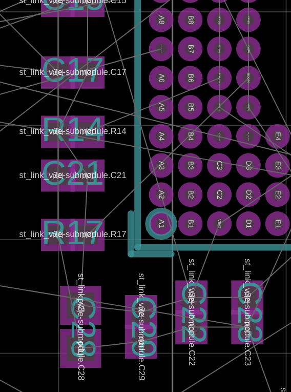 |
| Generic Capacitors, MIN-PKG = "1206" | 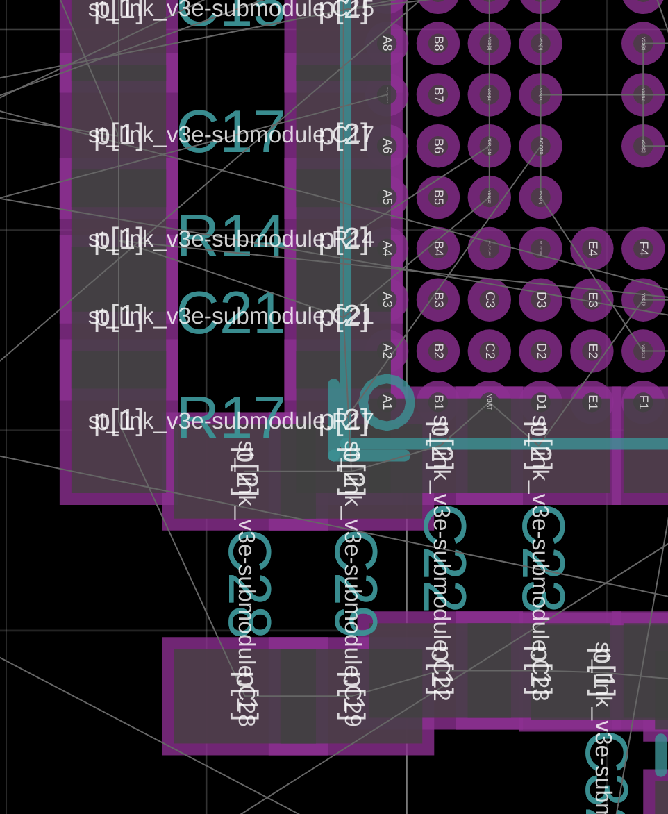 |
This manner of specifying capacitors more accurately describes the design intent than just specifying a manufacturer part number. As electrical engineers, we can specify only the important parameters and JITX will select a component that meets or exceeds the parameters based on stock and what we are optimizing for. Knowing what the import properties of a part are helps an organization support the product through its entire life cycle.
Change the resistors to generic, in-stock components
Once we're done with the capacitors, we can go through the same steps with resistors.
By swapping resistors with generic, in-stock components we:
- rapidly shrink (or expand) the components on the board
- eliminate out of stock resistors on the bill of materials
- and specify only the important parameters
The first 2 resistors we encounter, R33 and R34, have a 0.5% tolerance and is used to set the reference voltage. We can specify the tolerance for these. The other resistors can have no tolerance specified, and we can optimize for cost.
  public inst R33 : chip-resistor(10.0e3, 0.005)
  public inst R34 : chip-resistor(33.0e3, 0.005)
  public inst R35 : chip-resistor(180.0)
Remove jumpers and tie nets directly
This is a good time to check in our current status in our repository before going forward. In case we make a mistake, we can quickly revert to a working version.
We'll check in our code with:
git commit -am "Updated resistors and capacitors."
We're going to replace all the jumpers with net connections or leave them as opens. And, we'll comment out all the DNP components, enabling us to reduce BOM cost and shrink the board more.
To do this, we'll go through each pcb-module and compare it with the schematic page. The power module corresponds to page 6.
We will comment out SB5 (fitted) and SB14 (not fitted) by selecting each line and pressing Ctrl+/
Next, we will comment out the placements of each.
  public inst R7 : chip-resistor(510.0)
;   public inst SB14 : mb1367/rc0603jr-070rl/MCD-00071/component
;   public inst SB5 : mb1367/rc0603jr-070rl/MCD-00071/component
  public inst U11 : mb1367/ld1117s50tr/MCD-00088/component
  ...
  place(R7) at loc(59.5, 70.85, 180.0) on Top
;   place(SB14) at loc(48.59501, 24.19, 90.0) on Bottom
;   place(SB5) at loc(37.97, 41.84, 90.0) on Bottom
  place(U11) at loc(22.77, 43.615, 270.0) on Top
Finally, we'll modify the net statements (NetC51_2, VREF, NetC39_2, and p3V3 to connect the nets on each end of SB5 and remove references of SB5 and SB14.
Net p3V3 is modified to contain a reference to Net39_2.
net p3V3 (p3v3, JP6.COMMON, NetC39_2)
We will proceed the same way with the rest of the modules.
Update BGA land pattern
The microcontroller U5 land pattern has silkscreen around one of the BGA balls under the package and a big silkscreen box that could lift the component. We can see where the land pattern data for U5 is:
public inst U5 : mb1367/stm32f723iek6/MCD-00596/component
We can open up the file and search for silkscreen to find the silkscreen callouts. Then we can comment out the additional silkscreen. We will leave the two lines near pin 1 outside the box.
  ; layer(Silkscreen("F-SilkS", Top)) = Line(0.12, [
    ; Point(-4.25, 4.55),
    ; Point(-4.27283614024661, 4.66480502970953),
    ; Point(-4.33786796564404, 4.76213203435596),
    ; Point(-4.43519497029047, 4.82716385975339),
    ; Point(-4.55, 4.85),
    ; Point(-4.66480502970953, 4.82716385975339),
    ; Point(-4.76213203435596, 4.76213203435596),
    ; Point(-4.82716385975339, 4.66480502970953),
    ; Point(-4.85, 4.55),
    ; Point(-4.82716385975339, 4.43519497029047),
    ; Point(-4.76213203435596, 4.33786796564404),
    ; Point(-4.66480502970953, 4.27283614024661),
    ; Point(-4.55, 4.25),
    ; Point(-4.43519497029047, 4.27283614024661),
    ; Point(-4.33786796564404, 4.33786796564404),
    ; Point(-4.27283614024661, 4.43519497029047),
    ; Point(-4.25, 4.55)])
  ; layer(Silkscreen("F-SilkS", Top)) = Line(0.15, [Point(-5.075, -5.075), Point(-5.075, 5.075)])
  ; layer(Silkscreen("F-SilkS", Top)) = Line(0.15, [Point(-5.075, 5.075), Point(5.075, 5.075)])
  ; layer(Silkscreen("F-SilkS", Top)) = Line(0.15, [Point(5.075, -5.075), Point(5.075, 5.075)])
  ; layer(Silkscreen("F-SilkS", Top)) = Line(0.15, [Point(-5.075, -5.075), Point(5.075, -5.075)])
  layer(Silkscreen("F-SilkS", Top)) = Line(0.15, [Point(-5.225, 5.225), Point(-4.325, 5.225)])
  layer(Silkscreen("F-SilkS", Top)) = Line(0.15, [Point(-5.225, 4.325), Point(-5.225, 5.225)])
  ref-label()
Export the JITX Project to Altium
Follow the workflow outlined in Exporting JITX to Altium to bring your project back into Altium.
Update the layout
When we bring a project from JITX to Altium, it does not preserve the layout. This is simple to fix.
Remove the generated PcbDoc from the project. Right click on the PcbDoc, and select Delete
Copy the original PcbDoc into the new project folder.
Open the PcbDoc in Altium.
Drag the PcbDoc into the project.
Save the project file.
In the PcbDoc, select import changes from design. Check the changes and deselect any you don't want to make.
Altium Tip: We set which changes we would like to import by right-clicking on project document, going to ECO Options, and changing the settings. Typically, we don't want to import changes that remove layout rules like net colors and impedance control. We can also edit default ECO options in the project options.
We can now perform layout work. We can either unroute the design and shrink the whole board, or we can make another development board and just recenter the tracks to the smaller components.
We can see that the trace connections to component pads need adjusting, since we have smaller capacitors now:

Rapid changes we can make in JITX
Our first design will be another development board, so we set the design rules for larger land patterns that can be hand reworked if needed and large passive components. By changing one line of code, we can change all the passive components to be smaller size and the land patterns to be more dense. This will enable us to quickly go from development board to a packaged production design.
Development Board:
MIN-PKG = "0603"
DENSITY-LEVEL = DensityLevelA
Production:
MIN-PKG = "0201"
DENSITY-LEVEL = DensityLevelC
We can continue on this path and replace power supplies and reference voltages with solvers, and merge development boards into a single, integrated board using pcb-module.
Summary
In this tutorial, we imported a design from Altium, sourced alternate components for all of the capacitors and resistors, removed several components, and updated a land pattern. Simply by changing the resistor and capacitor calls, we went from a flat design specifying specific components, which may be obsolete or out of stock, to a stock-aware system. In other tutorials, we'll explore the additional benefits of software defined electronics.
Benefits:
- rapidly shrink the components on the board
- eliminate out of stock resistors and capacitors on the bill of materials
- specify only the important parameters
- quickly changed an evaluation board schematic to a production design
- improved land patterns