Modules
We have a good start on our design with models for the starting components of our transimpedance amplifier. Rather than just sticking the components in at the design level, we can define a reusable subcircuit that we can deploy any time we need a transimpedance amplifier.
This section shows you how to create reusable sub-circuits by using the pcb-module statement. Modules in JITX are collections of components, and other modules, connected by nets.
Let's define a reusable module for our transimpedance amplifier. Here is the target circuit
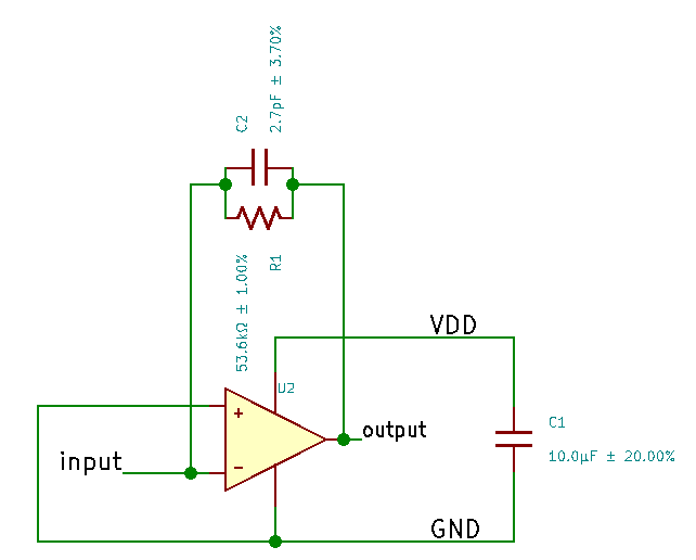
We start our module by transcribing this schematic into a netlist in a pcb-module:
pcb-module transimpedance-amplifier :
  pin input
  pin output
  pin vdd
  pin gnd

  inst op-amp:op-amp
  inst decoupling-cap : ceramic-cap(10.0e-6)

  ; Connect module pins and decoupling to op-amp power pins.
  net (vdd op-amp.v+ decoupling-cap.p[1])
  net (gnd op-amp.v- decoupling-cap.p[2])

  ; Add and connect feedback network
  inst r : chip-resistor(closest-std-val(54.0e3, 1.0))
  inst c : ceramic-cap(2.7e-12)

  net (gnd op-amp.in+)
  net (input, op-amp.in-, r.p[1] c.p[1])
  net (output op-amp.out, r.p[2] c.p[2])
This module starts with a definition of the ports -- when we use this module in our design, these ports are the only thing we connect to. Pins and ports are used interchangeably in this context.
inputis the input to the amplifieroutputis the output of the amplifiervddis our power pin.gndis our ground pin.
We then instantiate our op-amp and a decoupling capacitor:
  inst op-amp:op-amp
  inst decoupling-cap : ceramic-cap(10.0e-6)
ceramic-cap is a generic capacitor (similar to chip-resistor that we saw in the last section), here we request a 10.0uF ceramic capacitor.
Often a module will contain a key component and its housekeeping components. (e.g. the
pcb-modulefor the nRF52 contains the bypass capacitors, oscillators, and programming circuitry)
Next, we connect the op-amp to its decoupling capacitor, and importantly to the vdd and gnd pins on our module:
  ; Connect module pins and decoupling to op-amp power pins.
  net (vdd op-amp.v+ decoupling-cap.p[1])
  net (gnd op-amp.v- decoupling-cap.p[2])
Forgetting to connect up the gnd and vdd pins would mean that no connection would be made to the actual components, when we later instantiate this module and connect to its ports.
Finally we add the feedback resistor and capacitor, and connect them to our op-amp and the input and ouput pins:
  ; Add and connect feedback network
  inst r : chip-resistor(closest-std-val(54.0e3, 1.0))
  inst c : ceramic-cap(2.7e-12)

  net (gnd op-amp.in+)
  net (input, op-amp.in-, r.p[1] c.p[1])
  net (output op-amp.out, r.p[2] c.p[2])
We've picked some static values of ~54.0 kOhm and 2.7pF for our resistor and capacitor closest-std-val is a function from ocdb/utils/generic-components that gives the closest value in the EIA range applying to the tolerance we request. e.g. closest-std-val(54.0e3, 1.0) is the value closest to 54,000.0 in the 1.0% range and turns out to be 53,600.0.
Here is example code for this generator. We can add our transimpedance circuit to our design with a single inst statement:
pcb-module my-design :
  inst amp : transimpedance-amplifier
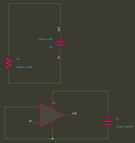
Which results in the correct, but slightly strange looking schematic:
Parameterization
Our module definition isn't too bad, but having the values for the feedback components hardcoded isn't great. Very often we want to make our modules parametric so they become more useful. Let's start by passing in our desired values for the resistor and capacitor:
pcb-module transimpedance-amplifier (rf:Double, cf:Double):
  pin input
  pin output
  pin vdd
  pin gnd

  inst op-amp:op-amp
  inst decoupling-cap : ceramic-cap(10.0e-6)

  ; Connect module pins and decoupling to op-amp power pins.
  net (vdd op-amp.v+ decoupling-cap.p[1])
  net (gnd op-amp.v- decoupling-cap.p[2])

  ; Add and connect feedback network
  inst r : chip-resistor(closest-std-val(rf, 1.0))
  inst c : ceramic-cap(cf)

  net (gnd op-amp.in+)
  net (input, op-amp.in-, r.p[1] c.p[1])
  net (output op-amp.out, r.p[2] c.p[2])
Now that our module is parametric, let's instantiate two versions of it with different gain resistors that will attach to two photodiodes. We also want a better schematic, so we add net symbols to the power and ground rails and apply logical groupings to the schematic.
pcb-module my-design :
  inst d : photodiode[2]
  inst high-gain-amp : transimpedance-amplifier(54.0e3, 2.7e-12)
  inst low-gain-amp : transimpedance-amplifier(27.0e3, 2.7e-12)
  inst connector : pin-header(3)

    ; Set up power connections
  net GND (high-gain-amp.gnd low-gain-amp.gnd connector.p[1])
  net VDD (high-gain-amp.vdd low-gain-amp.vdd connector.p[2])

  ; Connect diodes to amplifiers
  net (d[0].c high-gain-amp.input)
  net (d[0].a high-gain-amp.gnd)

  net (d[1].c low-gain-amp.input)
  net (d[1].a low-gain-amp.gnd)

  schematic-group(d[0]) = schematic-group(high-gain-amp)
  schematic-group(d[1]) = schematic-group(low-gain-amp)

  symbol(GND) = ocdb/utils/symbols/ground-sym
  symbol(VDD) = ocdb/utils/symbols/supply-sym
Here's a link to the complete tutorial code, which results in the new design:
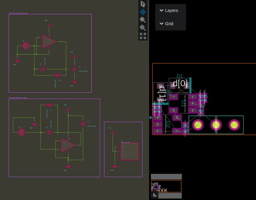
We now have two diodes connected to transimpedance amplifers that we instantiated using the same parametric module.
When we create parametric modules like this we usually start by transcribing some concrete schematic, and then gradually parameterize it until it captures the design space we care about. And modules can include each other, so this parametric amplifer could be used inside another module that generates and powers the entire analog front end. It's parametric reuse all the way down and all the way up, just like our parametric components.