Parametric CAD
We're going to need some generic parts like resistors and capacitors to finish out our design. In JITX these are generated parametrically, and this section is a deep dive on how that works.
JITX is embedded in a general purpose programming language, so we can write arbitrary software to generate circuitry. Instead of a creating a single design, we write reusable and parametric generators that generate whole families of designs.
Here's how that idea applies to a resistor:
pcb-component example-resistor :
  manufacturer = "Yageo"
  mpn = "RC0402FR-071KL"
  description = "RES SMD 1K OHM 1% 1/16W 0402"
  reference-prefix = "R"
  port p : pin[[1 2]]

  val sym = resistor-sym(ResistorStd)
  val lp = ipc-two-pin-landpattern("0402")
  symbol = sym(p[1] => sym.p[1], p[2] => sym.p[2])
  landpattern = lp(p[1] => lp.p[1], p[2] => lp.p[2])
Some new things here. example-resistor is annotated with a manufacturer, mpn, and a description - information used to build a bill of materials. Let's take a closer look at these four lines:
  val sym = resistor-sym(ResistorStd)
  val lp = ipc-two-pin-landpattern("0402")
  symbol = sym(p[1] => sym.p[1], p[2] => sym.p[2])
  landpattern = lp(p[1] => lp.p[1], p[2] => lp.p[2])
Both the symbol and the land pattern are created by parametric functions.
Here's an example generator to explore calling simple parametric generators for symbols and land patterns. Notice that we have imported
land-patternsandsymbolsfrom the library to bring in our previously written functions for generating land patterns and symbols. This generator useschip-resistor, a parametric resistor where we set the properties we care about (resistance, tolerance, power, etc...) and later an automated solver populates a BoM of real devices matching our requirements.
Parametric symbols
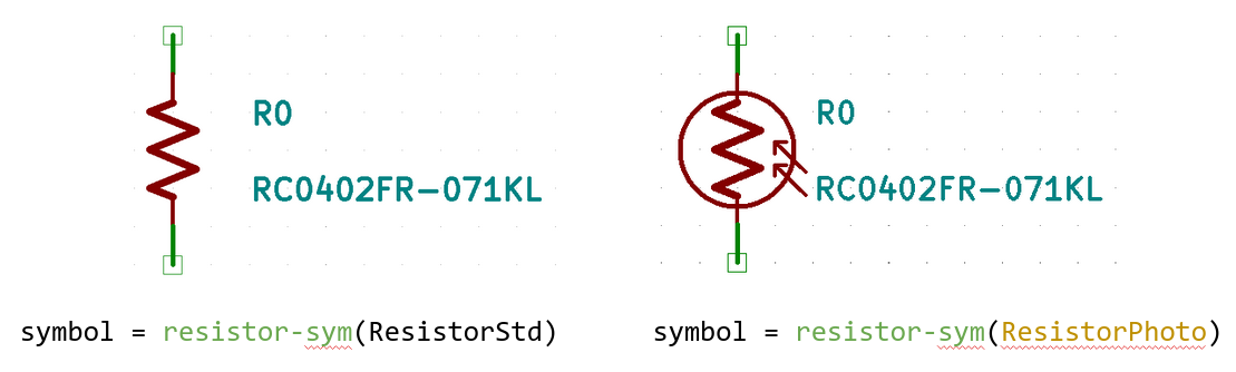
resistor-sym is a parametric pcb-symbol that generates different resistor symbols based on the type we request. resistor-sym(ResistorStd) produces a standard resistor symbol, but we could instead call resistor-sym(ResistorPhoto) to generate a photoresistor symbol, as shown below. Check out the implementation (defined in lib/utils/symbols.stanza) to see how the function works (use Go to definition to jump there).
We have written a whole suite of symbol generators, so it's quite rare that you would have to write your own from scratch.
Parametric land patterns
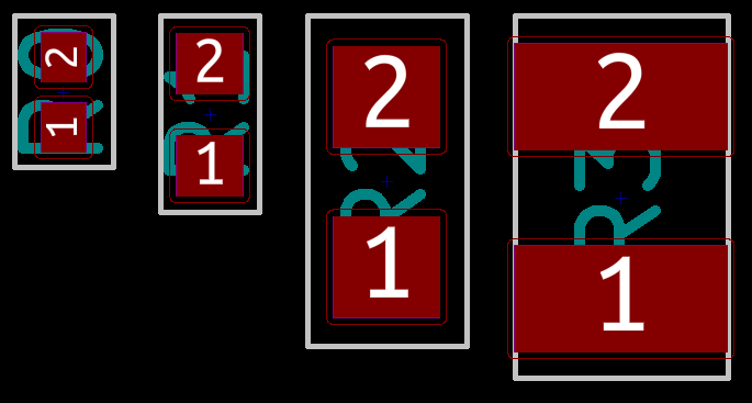
Similarly, ipc-two-pin-landpattern is a function that generates an IPC-compliant nominal material condition land pattern matching the requested land pattern size. Here are the results for 0201 - 0805:
Digging into the implementation of ipc-two-pin-landpattern, (found in lib/utils/land-patterns.stanza -- use Go to definition to jump there) shows how parametrization and reuse can be used to create families of land patterns. This code is heavily factored because each of the functions has standalone utility and gets used elsewhere.
The top-level function we call from our component creates a pcb-landpattern that is parameterized by a string indicating the land pattern size. Inside the land pattern there is a call to another function that will create the geometry based on the size argument.
public pcb-landpattern ipc-two-pin-landpattern (part-name:String) :
  make-ipc-two-pin-landpattern(part-name, true)
This function accepts a String as an input, that then matches that string to a set of parameters defining the land pattern geometry, and then pipes those parameters to a function that constructs the geometry. Notice that here we use inside pcb-landpattern : to set the context of this function to give us access to land pattern JITX statements.
public defn make-ipc-two-pin-landpattern (part-name:String, courtyard?:True|False) :
  inside pcb-landpattern :
    val [Z, G, X, nr, nc] = switch(part-name) :
      "0201" : [1.12, 0.20, 0.42, 1.42, 0.92]
      "0402" : [1.53, 0.39, 0.62, 1.84, 0.92]
      "0603" : [2.55, 0.65, 1.00, 3.10, 1.50]
      "0805" : [2.90, 0.90, 2.00, 3.40, 2.00]
      "1206" : [4.05, 1.65, 1.80, 4.60, 2.30]
      "2512" : [7.35, 4.85, 3.40, 3.90, 7.90]
      "1210" : [4.40, 1.20, 2.70, 5.00, 3.00]
      "2010" : [6.20, 2.60, 2.70, 7.00, 3.00]
      "2920" : [9.70, 5.10, 5.60, 10.0, 6.00]
      else : fatal("Unrecognized two pin part name: '%_." % [part-name])
    make-two-pin-landpattern(Z, G, X, nr, nc, courtyard?)
    ref-label()
This make-two-pin-landpattern function sizes and places pads based on the parameters we give it. Notice the smd-pad(Y,X) statements that construct parametrically sized pads.
public defn make-two-pin-landpattern (Z:Double, G:Double, X:Double, w:Double, h:Double, courtyard?:True|False) :
  inside pcb-landpattern :
    val Y = (Z - G) / 2.0 ; width of pad
    val C2 = (G + Y) / 2.0 ; distance between pad center and land pattern centerline
    pad p[1] : smd-pad(Y,X) at loc((- C2), 0.0)
    pad p[2] : smd-pad(Y,X) at loc(C2, 0.0)
    if courtyard? :
      layer(Courtyard(Top)) = Rectangle(w, h)
At the lowest level of hierarchy, we have the smd-pad function that creates a rectangular SMD copper pad with SolderMask and Paste layers. Here we use function overloading so if you call smd-pad with only a X-Y dimension, it sets a default anchor for you.
public defn smd-pad (w:Double, h:Double) :
  smd-pad(C,w,h)

public pcb-pad smd-pad (anchor:Anchor, w:Double, h:Double) :
  name = to-string("%_x%_ %_ SMD Pad" % [w,h,anchor])
  type = SMD
  shape = Rectangle(anchor, w, h)
  layer(Paste(Top)) = Rectangle(anchor, w, h)
  layer(SolderMask(Top)) = Rectangle(anchor, w, h)
It is rare that we have to dig this deep in the library in practice, but we hope the example drilling down to the lowest-level implementation details was illustrative.
Conclusion
To sum up, JITX code and much of OCDB (the JITX standard library) is made out of software functions that generate design information based on parameters. We get high levels of reuse, so we don't have to write much code to generate our designs and once we verify a generator, we know every design it produces will be correct. Also note that OCDB is open-source and yours to change and adapt to your own design preferences.
Furthermore, the native parametrization of JITX gives us a lot of power. Let's say that you would prefer smaller pads for each component to accomodate a dense design, or you want to make sure the soldermask dimensions on pads are adjusted when you are shipping a hi-rel aerospace design. Both are accomplished with a simple extension to the above code, and the change is rolled out globally when we change design parameters, without having to update each component manually.