Revising an Existing KiCad Design in JITX
In this tutorial, we will walk through modifying an existing KiCAD design in JITX by adding sourcing information to resistors and capacitors, adding an LED circuit, and editing a land pattern. Then, we'll export the design from JITX to KiCAD, and update the layout.
You'll need:
- KiCad
- A KiCad project
This tutorial uses the KiCAD files for the open source Goldfish design.
Contents:
- Import the KiCad Project to JITX
- Make changes to the project
- Export the JITX Project to KiCad
- Update the layout
- Rapid changes we can make in JITX
- Summary
Import the KiCad Project to JITX
Follow the workflow outlined in Importing KiCad to JITX to bring your project into JITX.
For this project, we used:
#use-added-syntax(jitx)
defpackage my-design :
  import core
  import jitx/commands

import-kicad("Goldfish/cad", "imported-Goldfish", [`overwrite => false])
Make changes to the project
Let's make the following changes:
- Set Project Parameters
- Change the Capacitors to find in-stock Components
- Change the Resistors to find in-stock Components
- Add a power LED
- Edit a land pattern
Let's open the generated file by pressing Ctrl+p and typing goldfish.stanza or double clicking on goldfish.stanza in the explorer window. Then go to File then Save As... and save it as promicro.stanza, because it is a variant of a Pro Micro Arduino.
We'll make edits to this new file. Having the original file will be useful in case we want to do a file compare on our changes later.
We'll visualize the imported design by opening the output folder in VSCode and running from the VSCode terminal:
jitx repl promicro.stanza
We can then rearrange our windows to see the generated code, the schematic, and the layout.
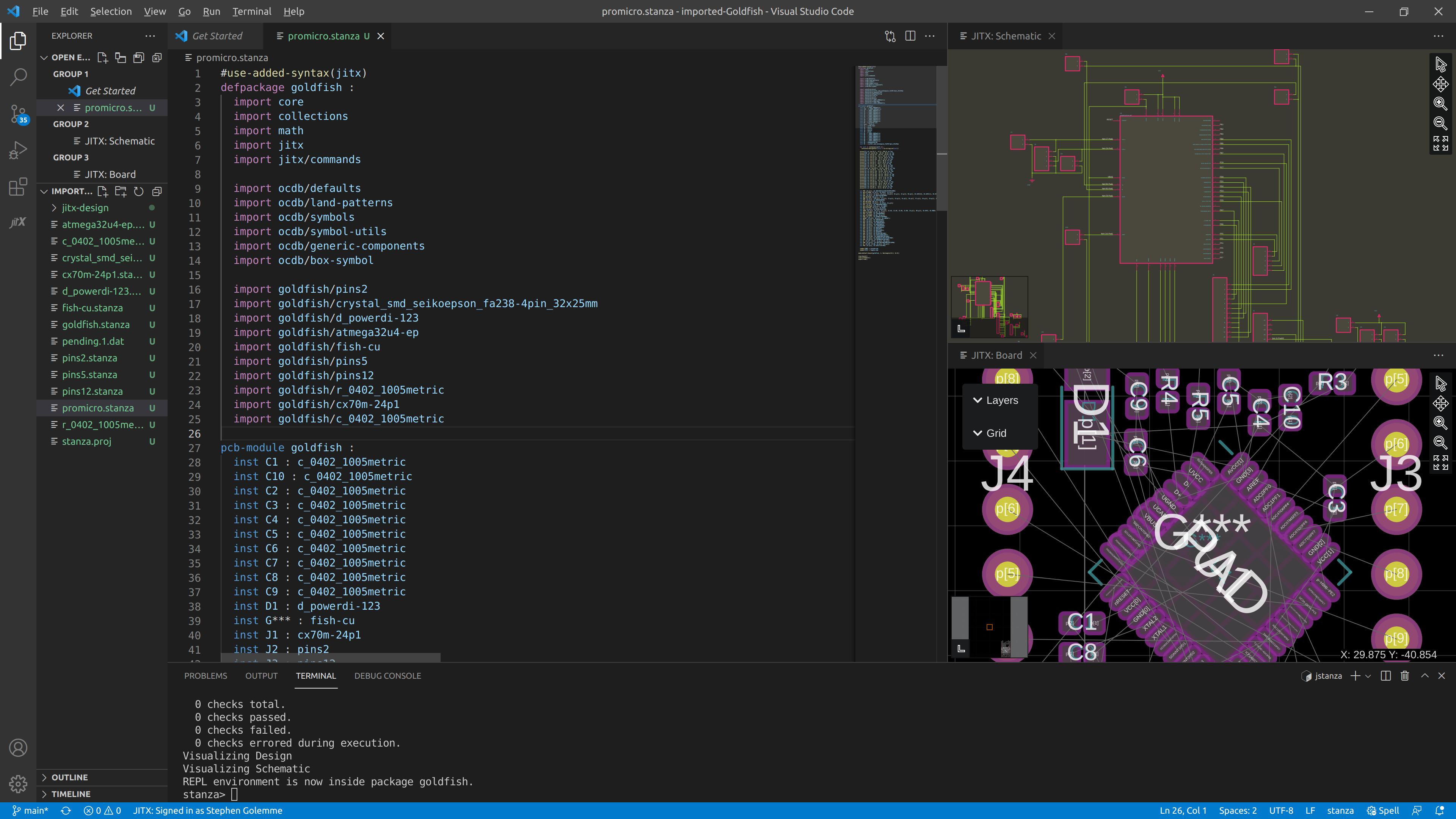
Tip: As we make changes, we can periodically test our code by saving
promicro.stanza, then typingreloadat the stanza prompt.
The last set of imports shows the components imported from KiCAD. A quick glance tells us that all of the resistors and capacitors are brought in as generic r_0402_1005metric or c_0402_1005metric.
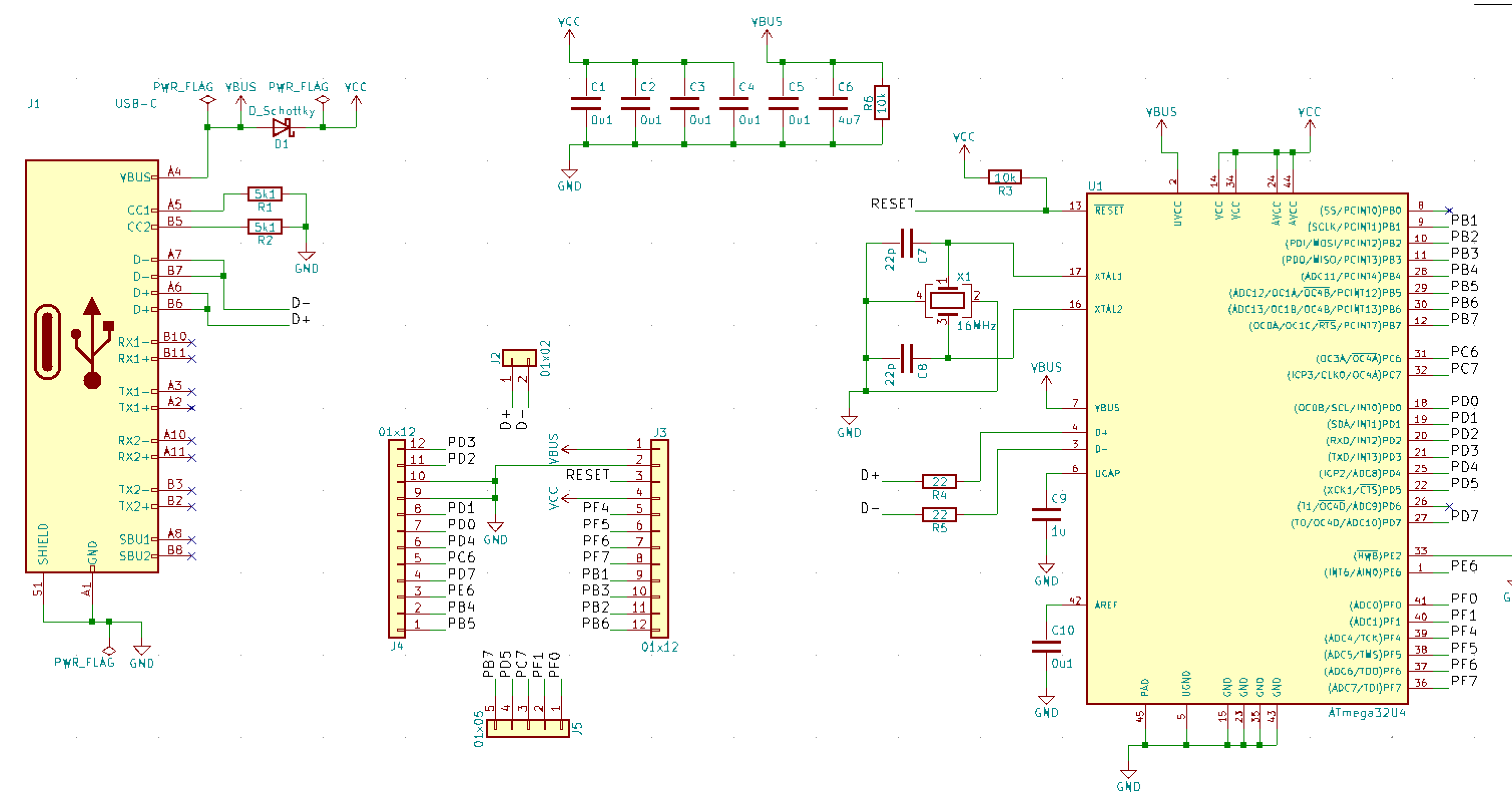
Let's start replacing them with JITX functions for capacitors and resistors that return manufacturer part numbers. We'll have to look at the KiCad schematic for the values that were manually added to each part.
The KiCad schematic:
Change the Capacitors to find in-stock Components
We can update each capacitor instance to use the ceramic-cap( function.
inst C9 : c_0402_1005metric
becomes
inst C9 : ceramic-cap(1.0e-6)
Since the maximum voltage on this board is 5 Volts (with the exception of Vin), We'll specify a project level minimum capacitor voltage of 10.0 volts, specifying a 100% headroom. We also specify a project level operating temperature. You can easily change inputs on a project level scale. If we're comfortable with less headroom, we can specify 6.3 Volts.
Right after the imports section of this file, We'll specify some project level parameters for package size, design quantity, and capacitor voltage. (note indentation):
  import ocdb/utils/design-vars
OPERATING-TEMPERATURE = min-max(0.0 40.0)
OPTIMIZE-FOR = ["area"]
MIN-PKG = "0402"
DESIGN-QUANTITY = 100
MIN-CAP-VOLTAGE = 10.0
This will select the cheapest capacitor that meets our specifications, 0402, with a minimum distributor stock to make 100 of this design, whenever a sourcing tool is called.
We can go through the rest of the design and replace capacitors in this manner. If we want to specify a higher minimum voltage for a specific capacitor, we can add "min-rated-voltage" => 25.0 to the capacitor function.
Change the Resistors to find in-stock Components
Let's update each resistor instance to use the chip-resistor( function.
inst R1 : r_0402_1005metric
becomes
inst R1 : chip-resistor(5.1e3)
Let's save and type reload followed by Enter in the command line to see the results.
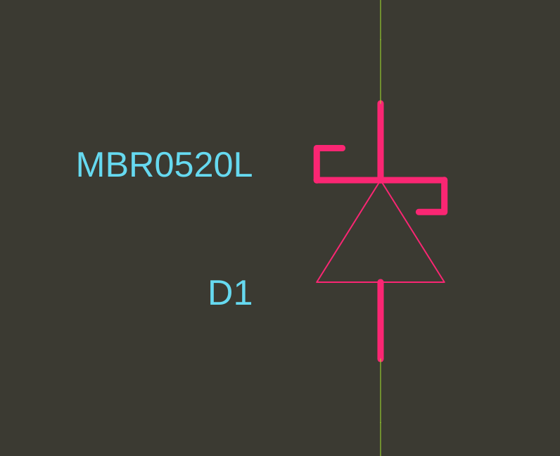
Replace the Schottky diode with one from OCDB
The diode D1 is a generic SOD-123 Schottky diode. We can search file contents for OCDB by pressing Ctrl+Shift+F and searching for schottky. Double-click on a result that's located in open-components-database/ that has SOD123 near the word Schottky. We can copy the MPN and see if it's in stock at our favorite distributor. And we can replace the D1 call with this component by copying the text after defpackage, then calling the component name.
inst D1 : d_powerdi-123
becomes
inst D1 : ocdb/components/on-semiconductor/MBR0520L/component
Let's save and type reload followed by Enter in the command line. to see the results. The command line returns [Error] Cannot access named field 'p'.
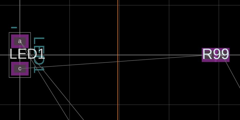
A search of promicro.stanza for D1 with a space before it shows 3 results: where D1 is instantiated, net VCC, and net VBUS. The pins are attached to the net with D1.p[1] and looking at the component we selected, we see the available pins are a and c. We'll change D1.p[1] to D1.c and D1.p[2] to D1.a, press Ctrl+S and then type reload and Enter. Now our design loads. It's also a bit easier to read that VCC is the cathode of the diode.
Add a power LED
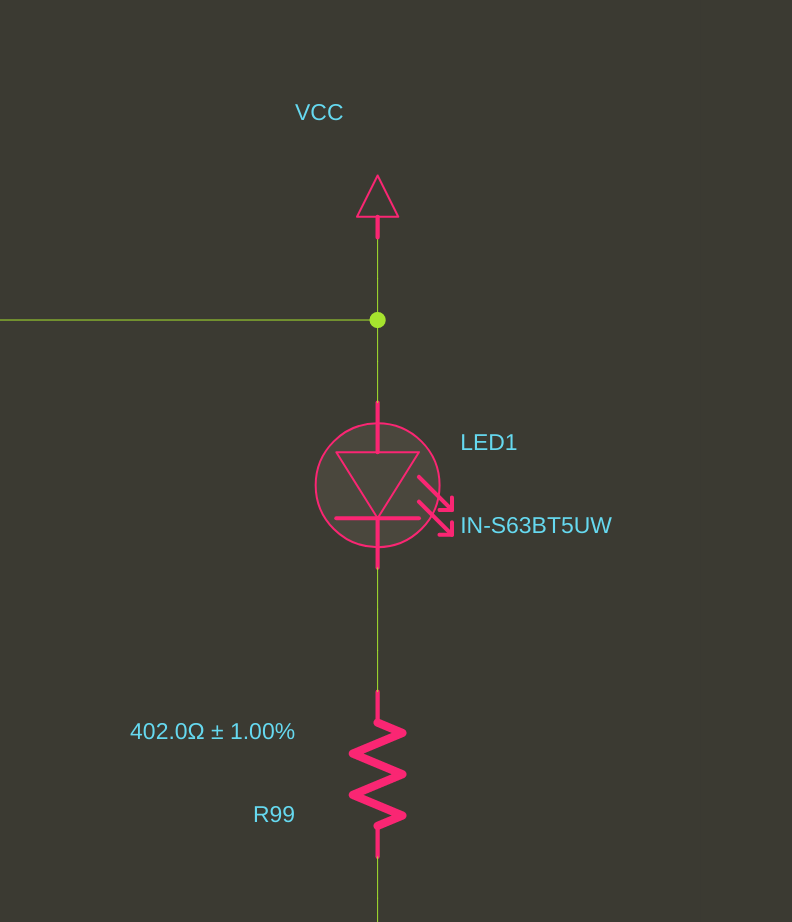
Next, we'll place a power LED circuit. Let's search for an in-stock 5mA 0603 LED on a distributor website and create a part. I found the Inolux IN-S63BT5UW to have a high mcd rating, 0603 package, 5mA, and a Vf of 3V.
We'll open one of the imported component files, d_powerdo-123.stanza, to quickly glance at what we need to create a component. Copy the contents of this file and press Ctrl+N to create a new file. Then paste the contents into this new file.
The second line defined the package name. Replace d_powerdi-123 with our new package name, IN-S63BT5UW. So the line reads:
defpackage goldfish/IN-S63BT5UW :
Then, press Ctrl+S to save the file. We'll save the file as IN-S63BT5UW.stanza.
Next, after public pcb-component change d_powerdi-123 to component so the line reads:
public pcb-component component :
Press Ctrl+S to save again.
To add an instance of this to promicro.stanza, we'll need to add links in 3 places. First, we need to tell the JITX Shell where to look to find this. Open stanza.proj in the imported-goldfish directory and add a line in the same format as the others:
package goldfish/IN-S63BT5UW defined-in "IN-S63BT5UW.stanza"
Don't forget to save! In promicro.stanza, add a new import statement at the end in the same format as the others:
import goldfish/IN-S63BT5UW`
Finally, after pcb-module goldfish :, add an instance of the part and place it at location 0.0, 0.0 with rotation 0.0 so we can easily find it and watch changes:
pcb-module goldfish :
  inst LED1 : goldfish/IN-S63BT5UW/component
  place(LED1) at loc(0.0, 0.0, 0.0) on Top
Note: We defined the LED model in a package named
goldfish/IN-S63BT5UWand in that package named the definitioncomponent. The full path of the component is<package>/<definition>and in this example:goldfish/IN-S63BT5UW/component
Save and type reload at the stanza prompt. If it reloads with no errors, we know we've tied everything together correctly.
Add a Land Pattern
Let's use the IPC land pattern generator for this part. First, open the datasheet to see what part dimensions are specified (we do not use the recommended land pattern):
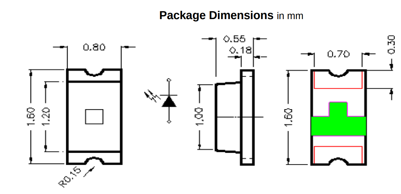
- length = 1.60
- width = 0.80
- lead-length = (1.60 - 1.20)/2 = 0.2
- lead-width = 0.70
- polarized =
true
Press Ctrl++P and open land-patterns.stanza by typing the filename in the box and pressing Enter when the file appears.
Then press Ctrl+F and search for two-pin-chip. Let's take a look at the first function that pops up. It take a lot of variables, and depending on if anode-and-cathode is true or false, will name the pins a and c or p[1] and p[2]. Then it computes a courtyard and draws an optional polarity marker.
We'll cycle through the different function calls until we see the one with only the inputs we want.
We find the following matches our inputs:
public defn make-two-pin-chip-landpattern (length:Toleranced,
                                           width:Toleranced,
                                           lead-length:Toleranced,
                                           lead-width:Toleranced
                                           polarized?:True|False):
The type of several inputs is Toleranced. We can see its reference documentation lists a function called tol ( that enables us to pass toleranced values. Since there are no tolerances given in the datasheet, we'll use a tolerance of 0.
Go back to the new file we're editing, IN-S63BT5UW.stanza. We'll change the name of the pcb-landpattern to IN-S63BT5UW-lp and replace all the indented code below it with the new function.
public pcb-landpattern IN-S63BT5UW-lp :
  make-two-pin-chip-landpattern(tol(1.6,0.0), tol(0.8, 0.0), tol(0.3,0.0), tol(0.7,0.0), true)
Tip: If we ever see the error,
Missing definition: There is a live object that requires the following definition:, this is due to a reference to something that is loaded into the JITX Shell that we have deleted. Kill the JITX Shell by typing Ctrl+C in the terminal and relaunch by pressing UpArrow then Enter.
The documentation for Toleranced shows us a function tol() that takes 2 or 3 values and returns the type Toleranced. We can go ahead and add all the values from the datasheet into the function.
Next, in pcb-component, we'll edit the pin properties to use pins and pads a and c and update the land pattern call in assign-landpattern(.
We don't want a box symbol for an LED, and there's likely an LED symbol somewhere in OCDB, we just have to find it! We can search for a component, or we can see if there's a standard symbol. We already import symbols and symbol-utils, so let's take a look and see if we can find an LED symbol in there.
Press Ctrl+Shift+F and search for defpackage ocdb/utils/symbols. Double click on the result to open the file. Now let's search the file for LED and press enter to cycle through the results.
We find public pcb-symbol diode-sym (d-type:DiodeSymbolType) : has a switch statement that accepts DiodeLED as an input, so let's do a Ctrl+Shift+F* search for diode-sym(DiodeLED) and see an example of it's use.
Since we deleted make-box-symbol(), we can remove import ocdb/utils/box-symbol as well.
We can check the JITX Reference on Component Statements and see different component properties we need to define. Let's add a few.
Finally, let's assign a property called vf of 3.0 to capture the forward voltage.
Here is the final code for our LED model:
#use-added-syntax(jitx)
defpackage goldfish/IN-S63BT5UW :
  import core
  import collections
  import math
  import jitx
  import jitx/commands

  import ocdb/utils/defaults
  import ocdb/utils/landpatterns
  import ocdb/utils/symbols
  import ocdb/utils/symbol-utils
  import ocdb/utils/generic-components
  import ocdb/utils/box-symbol

public pcb-landpattern IN-S63BT5UW-lp :
  make-two-pin-chip-landpattern(tol(1.6,0.0), tol(0.8, 0.0), tol(0.3,0.0), tol(0.7,0.0), true)
public pcb-component component :
  pin-properties :
    [pin:Ref | pads:Ref ...]
    [a | a]
    [c | c]
  val sym = diode-sym(DiodeLED)
  symbol = sym(self.a => sym.a, self.c => sym.c)
  assign-landpattern(IN-S63BT5UW-lp)
  name = "LED white 0603 3.0Vf 5mA"
  description = "LED WHITE CLEAR 0603 SMD"
  manufacturer = "Inolux"
  mpn = "IN-S63BT5UW"
  reference-prefix = "LED"
  property(self.vf) = 3.0
Let's add a resistor and net up the LED circuit. Since we defined the Vf property, we can get clever and make the value of this resistor calculated from that property and then rounded to the closest 5% resistor value. We'll place the resistor near the LED.
  inst R99 : chip-resistor(closest-std-val( (5.0 - property(LED1.vf)) / 5.0e-3,0.5))
  place(R99) at loc(10.0, 0.0, 0.0) on Top
Next, we'll add some net statements to connect everything. We could add pins to existing net statements, but grouping additions together makes for more readable code:
  net (GND R99.p[2])
  net (R99.p[1] LED1.c)
  net (LED1.a VCC)
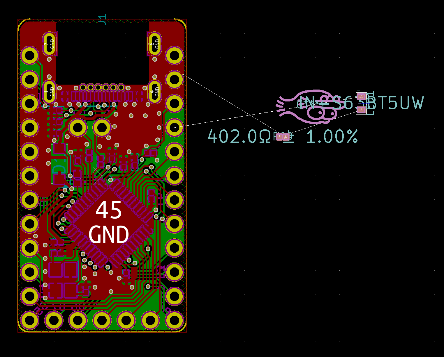
And the results of our 0603 LED and 0402 resistor:
 |  |
|---|
Edit a land pattern
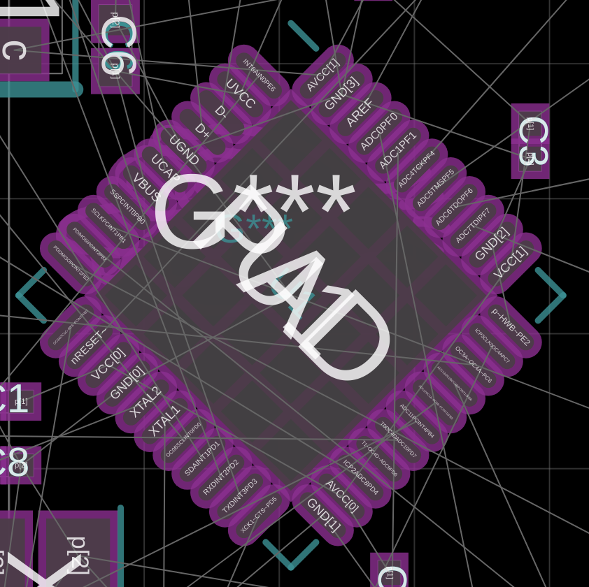
Microcontroller U1 has silkscreen on all 4 corners, and we would like only silkscreen by pin 1. Let's delete the silkscreen on the other corners. In promicro.stanza we see inst U1 : atmega32u4-ep. Let's open atmega32u4-ep.stanza and search for silk. We want to delete all the corners that have 2 silkscreen lines and leave the corner that has 1 silkscreen line. If we are unsure, we can comment out the silkscreen we think we want to delete, save and reload. If the display looks correct, we can permanently remove them. Comment out code by highlighting it and pressing Ctrl+/
  ; layer(Silkscreen("F-SilkS", Top)) = Line(0.12, [ Point(3.62, -3.62), Point(3.62, -2.95) ])
  ; layer(Silkscreen("F-SilkS", Top)) = Line(0.12, [ Point(3.62, -3.62), Point(2.95, -3.62) ])
  ; layer(Silkscreen("F-SilkS", Top)) = Line(0.12, [ Point(3.62, 3.62), Point(3.62, 2.95) ])
  ; layer(Silkscreen("F-SilkS", Top)) = Line(0.12, [ Point(3.62, 3.62), Point(2.95, 3.62) ])
  ; layer(Silkscreen("F-SilkS", Top)) = Line(0.12, [ Point(-3.62, -3.62), Point(-2.95, -3.62) ])
  ; layer(Silkscreen("F-SilkS", Top)) = Line(0.12, [ Point(-3.62, -3.62), Point(-3.62, -2.95) ])
  layer(Silkscreen("F-SilkS", Top)) = Line(0.12, [ Point(-3.62, 3.62), Point(-2.95, 3.62) ])
 |  |
|---|
Export the JITX Project to KiCad
Run export-cad()
The export backend defaults to KiCad.
Tip: More information on the export tool is in the JITX Reference - Export
Update the layout
When we bring a project from JITX to KiCad, it does not preserve the layout. This is simple to fix.
Copy the name of the generated kicad_pcb file and then delete it.
Copy the original kicad_pcb file into the new project folder.
Change the name of the kicad_pcb to the generated name.
Open the KiCad pro file. We should see a `kicad_pcb file in the project.
Open the kicad_pcb file.
Select Tools then Update PCB from Schematic...
Set the Match Method to Re-associate footprints by reference and check the Option to Update footprints
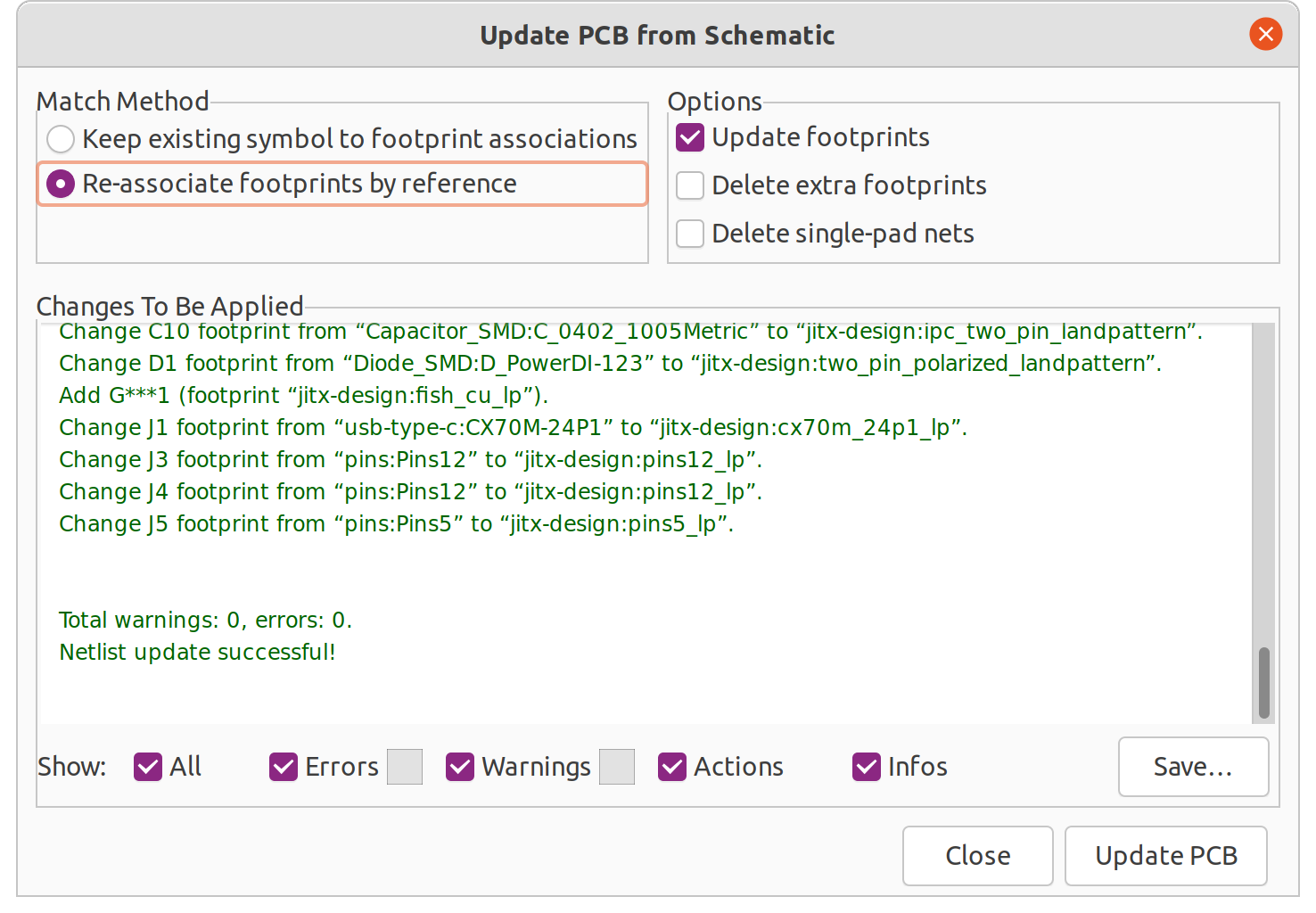
Press Update PCB
We should see the new parts we added. Also, due to the unusual reference designator of the Goldfish artwork, we may see that it moved.
We can now update the layout. We can either unroute the design and shrink the whole board, or we can make another development board and just recenter the tracks to the smaller components.
Rapid changes we can make in JITX
Our first design will be a development board we can order, and maybe our second design will be an even smaller board. We set the design rules for larger or smaller land patterns depending on what we're trying to accomplish. By changing one line of code, we can change all the passive components to be smaller size and the land patterns to be more dense. This will enable us to quickly go from development board to a packaged production design.
Development Board:
MIN-PKG = "0603"
DENSITY-LEVEL = DensityLevelA
Production:
MIN-PKG = "0201"
DENSITY-LEVEL = DensityLevelC
We can continue on this path and merge this board with another pcb-module to make a single, integrated board.
Summary
In this tutorial, we imported a design from KiCad, sourced alternate components for all of the capacitors and resistors, added a power LED circuit, and updated a land pattern. Simply by changing the resistor and capacitor calls, we went from a flat design that did not specify component part numbers, creating a lot of tedious work for us, to a stock-aware system. In other tutorials, we'll explore the additional benefits of software defined electronics.
Benefits:
- rapidly shrink the components on the board
- eliminate out of stock resistors and capacitors on the bill of materials and source in stock components
- specify only the important parameters
- quickly changed an evaluation board schematic to a production design
- improved land patterns