Bundles
A pcb-bundle is a collection of pins. Usually we create bundles to group pins that we want to keep together. For example we can create a bundle for an i2c bus with the following statement:
pcb-bundle i2c:
  pin sda
  pin scl
When to Use Bundles
Bundles are useful when you have any system which has multiple connections that you want to connect at once, such as:
- connectors
- busses
- GPIO
- protocols (SPI, I2C, etc.)
Tutorial
Now that our photodiodes are in order, we want to quickly bring up the rest of our design, which will be connected with interfaces like i2c and spi. We manage those connections in JITX using bundles.
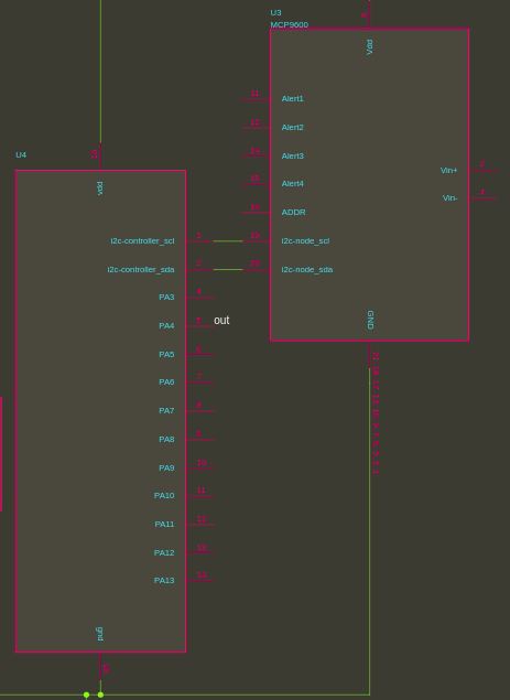
We can use our new bundle to define i2c interfaces on components and wire them up. For example, let's say we want to connect a thermocouple amplifier to a microcontroller using an i2c bus.
pcb-component thermocouple-amplifier :
  manufacturer = "Microchip"
  mpn = "MCP9600"
  description = "Thermocouple EMF to Temperature Converter, ±1.5°C Maximum Accuracy"
  port i2c-node : i2c
  pin-properties :
    [pin:Ref      | pads:Int ...         | side:Dir     ]
    [GND      | 1, 3, 5, 6, 7, 9, 10, 13, 17, 18, 21 | Down  ]
    [Vin+     | 2               | Right   ]
    [Vin-     | 4               | Right   ]
    [Vdd      | 8               | Up      ]
    [Alert[1] | 11              | Left    ]
    [Alert[2] | 12              | Left    ]
    [Alert[3] | 14              | Left    ]
    [Alert[4] | 15              | Left    ]
    [ADDR     | 16              | Left    ]
    [i2c-node.scl  | 19         | Left    ]
    [i2c-node.sda  | 20         | Left    ]

  make-box-symbol()
  assign-landpattern(qfn-landpattern(0.65, 5.0, 20, 0.3, 0.4, [3.25 3.25]))

pcb-component microcontroller :
  port i2c-controller : i2c
  pin-properties :
    [pin:Ref | pads:Int ... | side:Dir]
    [i2c-controller.scl   | 1 | Right]
    [i2c-controller.sda   | 2 | Right]
    for i in 3 to 14 do :
      [PA[i]   | i + 1 | Right]
    [vdd       | 15 | Up]
    [gnd       | 16 | Down]
  make-box-symbol()
  assign-landpattern(soic127p-landpattern(16))

pcb-module my-design :
  inst K : thermocouple-amplifier
  inst mcu : microcontroller
  net (K.i2c-node, mcu.i2c-controller)

  inst high-sensitivity-photodiode : amplified-photodiode(photodiode, 3.3, 500.0,  1.0e6)
  net (high-sensitivity-photodiode.output mcu.PA[4])
In our thermocouple-amplifier component, port i2c-node : i2c defines a port named i2c-node and sets the type to be i2c. i2c-node now has the two pins from the i2c bundle, sda and scl. We can then assign the pins of the i2c-node port to concrete land pattern pads.
We then add a similar port to the MCU named i2c-controller and assign it to concrete pads on the land pattern.
After we instantiate these components in our design, we can directly connect the i2c ports together using the net statement. JITX does the work to go into the bundle and connect scl to scl and sda to sda, so at the end of the day pin 19 on the light sensor gets connected to pin 1 on the micro controller.
This direct connection works with bundles of identical type, no matter how complex. It's an easy way to reduce errors in our design - when we connect i2c ports there is no way to accidentally connect sda to scl.
Here's a link to the complete tutorial code you can run to produce this design. Here is a portion of the schematic showing our i2c connection:
Complex bundles
pcb-bundles can include other bundles hierarchically, with as many layers of hierarchy as we need. Let's create a bundle for a DDR3 interface.
pcb-bundle diff-pair:
  pin P
  pin N

pcb-bundle ddr3-data :
  port ck : diff-pair
  port ldqs : diff-pair
  port udqs : diff-pair
  port ba : pin[3]
  port a : pin[15]
  port dq : pin[16]
  pin cke
  pin odt
  pin nCS
  pin nRAS
  pin nCAS
  pin nWE
  pin dmu
  pin dml
  pin nRESET

pcb-bundle ddr3-power :
  pin vddq
  pin vssq
  pin vdd
  pin vss
  pin vrefdq
  pin vrefca
  pin zq

pcb-bundle ddr3 :
  port data  : ddr3-data
  port power : ddr3-power
We first define a bundle for a differential pair, with pins N and P. We then use that bundle inside a new ddr3-data bundle for the DDR3 clock, and data strobes. The ddr3 data bundle also includes banks of address and data pins and the control pins. We then create a ddr3-power bundle with the supply and reference voltages. Finally we wrap ddr3-data and ddr3-power up into a single ddr3 bundle.
We can still access the low-level pins using the . operator: ddr3.data.ck.P gets us the positive pin of the DDR3 clock. (ddr3.data.clk would get us the differential pair). More importantly, we don't have to fuss with the low-level pins because we can net the top level bundles together:
net (FPGA.ddr3, SDRAM.ddr3)
This net statement connects a total of 56 pins from an FPGA to your SDRAM, making sure everything is connected correctly by recursively connecting all of the sub-bundles.
(You can create parametric bundles if you wanted to capture the full scope of all possible DDR3 connections (x4 x8, etc...).)