Land patterns and symbols
We can use JITX to generate a complete CAD package from our generator code. To generate a board design from our generator, each component we include needs to have an associated land pattern. To generate a schematic, each component also needs to have an associated symbol.
This section shows you how to work with low-level land pattern and symbol definitions. In practice we generate pads, land patterns, and symbols programmatically (as you will see in the next section), but this section will give you the foundations to understand what it being generated. Example code for this section is here.
Land Patterns
We use land patterns to model the geometry that attaches a component to a board. We create a land pattern using the pcb-landpattern statement and add pads to it using the pad statement. Let's define a land pattern for our three-pin-header from the previous section.
Let's first define a pad named round-pth-pad. This is a plated through-hole pad, the copper shape is a circle with an 0.8mm radius and the hole has an 0.5mm radius. We define SolderMask layer of the same shape top and bottom to go along with the copper pad.
pcb-pad round-pth-pad :
  type = TH
  shape = Circle(0.8)
  layer(Cutout()) = Circle(0.5)
  layer(SolderMask(Top)) = Circle(0.8)
  layer(SolderMask(Bottom)) = Circle(0.8)
Next we define a land pattern for our pin-header that includes three of these round-pth-pad pads.
pcb-landpattern pin-header-landpattern :
pad p[1] : round-pth-pad at loc(-2.54, 0.0)
pad p[2] : round-pth-pad at loc(0.0, 0.0)
pad p[3] : round-pth-pad at loc(2.54, 0.0)
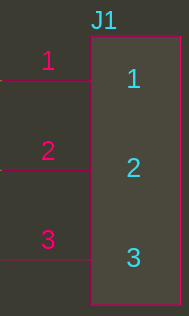
layer(Courtyard(Top)) = Rectangle(6.6, 1.6)
layer(Silkscreen("values", Top)) = Text(">REF", 0.7, C, loc(0.0, -1.2))
pad p[1] : round-pth-pad at loc(-2.54, 0.0) translates to 'create a pad named p[1] of type round-pth-pad, and place it at location x = -2.54mm, y = 0.0mm'.
Notice that we started our pad numbers at 1 (instead of 0) so they would more closely match a real component. We also define a courtyard to define the extents of the land pattern, and place a reference designator on the top silkscreen layer.
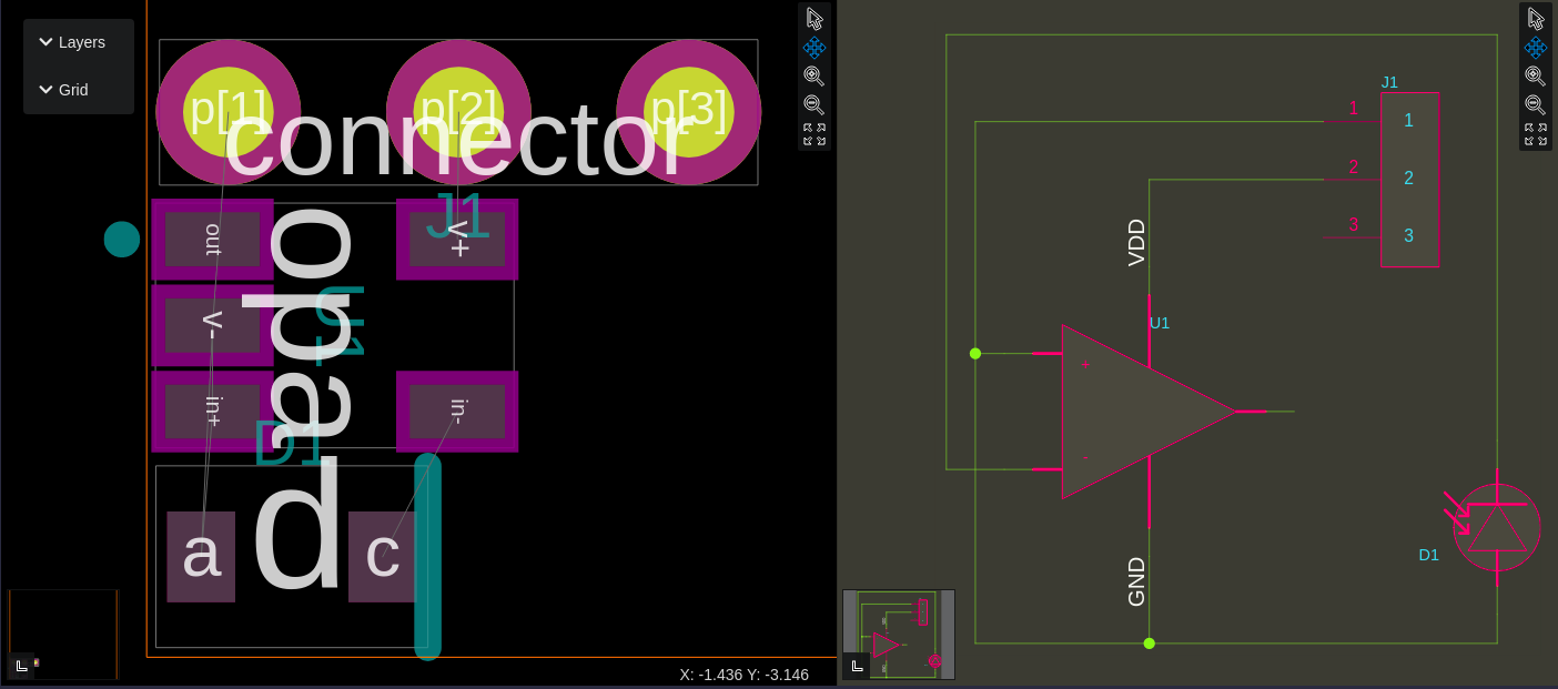
Here is the resulting geometry:

Finally we associate pin-header-landpattern with our three-pin-header component from the previous section:
pcb-component three-pin-header :
  port p : pin[[1 2 3]]
  landpattern = pin-header-landpattern(p[1] => pin-header-landpattern.p[1]
                                       p[2] => pin-header-landpattern.p[2]
                                       p[3] => pin-header-landpattern.p[3])
Notice that we updated to port definition to have pins p[1] p[2] and p[3] to match the land pattern (instead of starting at p[0]).
landpattern = pin-header-landpattern(p[1] => pin-header-landpattern.p[1] translates to:
- The land pattern associated with
three-pin-headerispin-header-landpattern - Pin
p[1]on the component maps to padp[1]onpin-header-landpattern.p[2]maps top[2],p[3]top[3].
So a component definition includes a reference to a land pattern, as well as a mapping that connects component ports to land pattern pads. When we instantiate a component, we can only connect to the components ports -- not the pads on the land pattern.
Symbols
Lastly, we need to define a symbol for our pin-header and associate it with our component. Here is a symbol definition for our header:
pcb-symbol pin-header-symbol :
  layer("foreground") = Rectangle(2.54, 7.62, loc(-1.27, 0.0))
  for i in 0 to 3 do :
    pin p[(i + 1)] at Point(-2.54, (2.54 - (to-double(i) * 2.54))) with :
      direction = Left
      length = 2.54
      number-size = 0.762
      name-size = 0.762
  layer("reference")  = Text(">REF", 0.7056, W, loc(-2.54, 4.2))
  preferred-orientation = PreferRotation([0])
First we add a graphic rectangle to our symbol:
layer("foreground") = Rectangle(2.54, 7.62, loc(-1.27, 0.0))
Then we use a for loop to place three pins on our symbol. The pin statements create connection points on the schematic. In the for loop, when i = 0, this snippet
pin p[(i + 1)] at Point(-2.54, (2.54 - (to-double(i) * 2.54))) with :
      direction = Left
      length = 2.54
      number-size = 0.762
      name-size = 0.762
Creates a pin named p[1] and places it at x = 2.54mm, and y = 2.54mm, sets the direction of the pin to face the left side, sets the length of the pin, and sets font sizes for the labels. To export to CAD correctly, we must use a 2.54mm grid for placing symbol pins. Graphics can be anywhere, but the pins have to be on that 2.54mm grid to be compatible with traditional CAD tools.
This line: layer("reference") = Text(">REF", 0.7056, W, loc(-2.54, 4.2)) sizes and places text for the reference designator. And finally we don't want to allow the schematic drawing algorithms to rotate this symbol, so we lock it in with preferred-orientation = PreferRotation([0]).
And this is how our pin-header-symbol looks:
Finally we associate pin-header-symbol with our component, and map the component pins to the symbol pins.
pcb-component three-pin-header :
  port p : pin[[1 2 3]]
  landpattern = pin-header-landpattern(p[1] => pin-header-landpattern.p[1]
                                       p[2] => pin-header-landpattern.p[2]
                                       p[3] => pin-header-landpattern.p[3])
  symbol =           pin-header-symbol(p[1] => pin-header-symbol.p[1]
                                       p[2] => pin-header-symbol.p[2]
                                       p[3] => pin-header-symbol.p[3])
  reference-prefix = "J"
We also set the reference prefix of this component to be "J" (JITX defaults to "U" if the reference prefix is unspecified).
More examples
We're going to add land patterns and symbols for our op-amp and photodiode as well, but take the more usual approach of drawing on some pre-written functions to generate the symbols and land patterns. The Open Components Database (OCDB), is a library of component models, reusable circuits, example designs, and utilities to make it easy to build new designs using JITX. We're going to import symbol and land pattern generators from OCDB to do some work for us.
Here is example code for this section. (You can run this generator using the instructions in Your first JITX design). In the front matter of that program you can see the new import statements
  import ocdb/utils/symbols
  import ocdb/utils/box-symbol
  import ocdb/utils/landpatterns
  import ocdb/utils/defaults
Here is the model for our photodiode:
pcb-pad rect-smd-pad :
  type = SMD
  val pad-shape = Rectangle(0.75, 1.0)
  shape = pad-shape
  layer(SolderMask(Top)) = pad-shape
  layer(Paste(Top)) = pad-shape

pcb-landpattern polarized-chip-landpattern :
  pad a : rect-smd-pad at loc(1.0, 0.0)
  pad c : rect-smd-pad at loc(-1.0, 0.0)
  layer(Courtyard(Top)) = Rectangle(3.0, 2.0)
  layer(Silkscreen("pol", Top)) = Line(0.30, [Point((- 1.5), (- 1.0)) Point((- 1.5), 1.0)])
  layer(Silkscreen("values", Top)) = Text(">REF", 0.7, C, loc(0.0, -1.2))

pcb-component photodiode :
  pin a
  pin c
  landpattern = polarized-chip-landpattern(a => polarized-chip-landpattern.a,
                                           c => polarized-chip-landpattern.c)
  val sym = diode-sym(DiodePhoto)
  symbol =                             sym(a => sym.a,
                                           c => sym.c)
  reference-prefix = "D"
We defined the land pattern from scratch just to give another example, but the symbol comes from the parametric diode-sym generator in ocdb/utils/symbols.
val sym = diode-sym(DiodePhoto) creates a photodiode symbol for us (this symbol was built with utilities in OCDB that manage the grid correctly).
Here is the model for the op-amp :
pcb-component op-amp :
  pin-properties :
    [pin:Ref | pads:Int ...]
    [in+     | 3 ]
    [in-     | 4 ]
    [out     | 1 ]
    [v+      | 5 ]
    [v-      | 2 ]
  assign-landpattern(SOT95P280X145-5N)
  symbol = op-amp-sym(self.in+ => op-amp-sym.in+
                      self.in- => op-amp-sym.in-
                      self.out => op-amp-sym.out
                      self.v-  => op-amp-sym.v-
                      self.v+  => op-amp-sym.v+)
We use the pin-properties syntax to create pins and map them to the landpattern at the same time. [in+ | 3 ] creates the component pin in+, and maps it to p[3] on a landpattern.
assign-landpattern(SOT95P280X145-5N) associates the pin assignment with a pre-defined SOT land pattern from ocdb/utils/landpatterns.
The op-amp-sym symbol comes from ocdb/utils/symbols.
And when we run the generator, we can now see a schematic and layout for our design:
Now that we have land patterns and symbols, CAD can now be exported from this generator.
This section showed you how to create the lowest-level land patterns and symbols and associate them with components. In practice, we spend very little time creating land patterns and symbols like this. Almost everything is generated from a reusable parameterized function, as you will see in the next section.