Pours
"Pours" fill available space in a region with copper. For nets that need to connect to many different components, a single pour can replace many point-to-point traces. Pours may also distribute power more effectively because they have lower impedance (since they are typically wider than traces), and may help with thermal management by better distributing heat.
JITX provides two different ways to define pours: * Code placed pours: These are pours added with copper-pour statements * Dynamic pours: These are pours created during board layout by configuring a trace as a pour
Code placed pours will typically allow more specific geometry, particularly for defining the transitions from one pour to another. They are also specified programmatically so, e.g. they can be included in modules to ensure they are included any time an instance of that module is used. Code placed pours are a good choice for power or ground plains that fill an entire layer of the board. They are also a good choice for things like shielding or thermal pours that should cover a specific region. The region for code placed pours is a user defined shape such as a Rectangle or Polygon.
Dynamic pours fill regions around traces that are configured as 'generators'. Dynamic pours are a good choice for adding extra width to traces that might carry a lot of current. They can be a good if you need to split a layer into many power planes with a complex boundary. Dynamic pours are computed by dividing up the board based on the closest selected trace. This means that the area between two generator traces will be evenly shared.
Input shapes and computed shapes
The shape specified in code placed pours and the regions computed for dynamic pours are considered 'input shapes'. However, these input shapes will almost always overlap with pads, traces, and other features on the board. To avoid this, only available parts of the input shapes will actually be filled with copper. If a clearance is necessary between a pour and any other feature on the board, the pour will be trimmed rather than adjusting the other feature. This means space will be left around traces, pads, etc. (unless they are part of the same net as the pour). In addition narrow slivers and sharp exterior corners will be removed from pours. If the input shapes of two or more pours overlap, the pour with the lowest rank will be trimmed. Note: If two pours of equal rank overlap, isolate regions will be removed from both so it is typically good to have unique ranks for all pours!
The remainder after the steps above is the 'computed shape' which is what will actually be fabricated when manufacturing a board. The 'computed shape' is what is displayed in the UI and used to check connectivity.
'input shapes' are what will be exported to other ECAD tools.
Reinterpretation of exported pours
Users should be aware that there is significant variation in how different ECAD tools interpret pours. While JITX attempts to ensure compatibility, it is a good idea to verify that external tools have computed equivalent pour shapes in any geometrically sensitive areas. e.g. this can be particularly important if pours have narrow regions where connectivity may be cut off or thermals may not be fully inside of pours. We are actively working to develop higher fidelity export targets.
Code Placed Pours Example
Some typical code placed pours might look like this:
  ; Use the bottom side of the board as a ground plane
  geom(GND) :
    copper-pour(LayerIndex(0, Bottom), isolate = 0., rank = 1) = Rectangle(board-width,board-height)
  ; Use a strip along the right edge of the board for power
  geom(VDD) :
    copper-pour(LayerIndex(0, Bottom), isolate = 0.5, rank = 2) = Rectangle(10, board-height, loc(board-width - 5., 0.))
Some things to note:
- These input shapes overlap, but since the ground pour has a lower rank the power pour will take priority
- Even though the isolate value for the ground pour is zero, other clearance rules will still apply
See copper-pour statements for full details.
Dynamic Pours Example
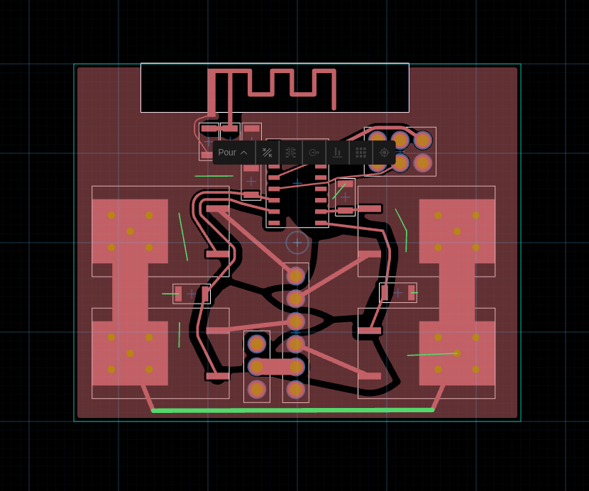
Dynamic pours are created in the physical design GUI. To make one, select a trace from the desired net and select "Pour" from the mode options.
Tips and tricks: * Dynamic pours always have a rank of 10. You can mix dynamic and code placed pours by using a rank greater than 10 * "Trace Width" controls the minimum feature size for the pour. Setting a larger value will round more off of corners and trim away more slivers. * Touching dynamic pours on the same net (i.e. generated from two neighboring traces) will use the largest clearance value. It is not possible to have different clearance values for different parts unless they are separated by something else.
You can combine many different dynamic pours on the same net to get more fine grained control of pour shapes. In this example, several traces (highlighted in green) were added and configured as pours to corral the 4 high current pours in the middle of the board.
Pour shape computation details
Dynamic pours more or less work as follows: * Collect all of the traces configured as dynamic pours * Label each region on the board based on which of those traces is closest * Combine any adjacent regions that are part of the same electrical net * Add a gap between any adjacent regions that are part of different nets based on needed clearance * The remaining regions will then be handled the same as 'input shapes' from code generated pours
Computed shapes more or less work as follows: * Consider each pour (code generated and dynamic) from highest to lowest rank * Start with the input shape * Add a gap around any features on the board that need to be isolated from the pour * Trim away any parts of the pour outside of the board boundary * Remove any thin regions and round off any sharp corners * The remaining shape is the 'computed shape' and is added as an obstacle for lower ranked pours to isolate from
Pour limitations
The following features are currently on our product roadmap but are not yet available:
- Direct editing of pour input shapes
- Generate thermal cutouts around pads as part of computed pour shapes
- Higher fidelity export targets
- More visualization options in board layout to, e.g. show input shapes or unconnected orphans
Pour behaviors tidbits
- If two or more overlapping pours have the same rank neither wins. i.e. isolate regions for pours with the same rank will be computed based on the full input shape of overlapping pours.
- The pin assignment solver does not consider potential connections to pours when selecting assignments. This ensures that pours will typically not restrict options for which traces can be added. e.g. suppose there is a require pin on the same net as a pour; possible support pins will be isolated from that pour until a trace is added from the support pin to something else on that net; after that trace is added (making it unambiguous which support pin should be used) the isolate region will be removed and the pour will be allowed to overlap the support pin.
- Pours are not considered by autorouter and may be cut into disconnected pieces by traces going through them. If you wish to ensure a contiguous connection between two points you can add a trace on top of the pour.
- Pours are not allowed to connect to topologies. Pin assignment will automatically add restrictions to prevent pours from being connected to topologies. If a trace that is already part of a topology is configured as a pour (this is not officially supported), the trace will be isolated from its own generated pour.