Substrate & Stackup#
The Substrate is a class that encapsulates the stackup, fabrication constraints, routing structures, vias, and other physical features that define the primitives of a PCB design. This class is intended to be included at the top-level of a design and be referenced at any point in the design tree. This allows both the end-user and library developers to reference the substrate when programmatically constructing circuits and layouts.
Substrate#
If we reference the SampleSubstrate, we can see the basic structure for a substrate:
class SampleSubstrate(Substrate):
  """Sample substrate using a two layer stackup and the sample fabrication
  constraints."""

  stackup = SampleTwoLayerStackup()
  constraints = SampleFabConstraints()

  class MicroVia(Via):
    ...

  RS_50 = RoutingStructure(
    impedance = 50 * ohm,
    layers = symmetric_routing_layers(...)
  )

  DRS_100 = DifferentialRoutingStructure(
    name = "100 Ohm Differential Routing Structure",
    impedance = 100 * ohm,
    layers = symmetric_routing_layers(...)
  )
The stackup and constraints attributes are required for a substrate. The via and routing structure definitions are optional features. We can add as many via definitions as needed for our design.
The routing structures are registered with the substrate associated with a characteristic impedance. The idea is that the user can use the routing_structure and differential_routing_structure methods to lookup routing structures by impedance. In this example, we have a 50Ω single-ended and a 100Ω differential routing structure. For example:
import jitx

class SomeCircuit(jitx.Circuit):

  def __init__(self):
    rs = jitx.current.substrate.routing_structure(50.0)
The idea here is that we can abstract the details of a particular substrate from the code that needs to know about vias, routing structures, and other primitives. The routing_structure method allows us to query the substrate for the current design for an impedance controlled structure. Whether you are writing a custom circuit for this design, or are developing a general use library to be used in many designs, this provides a common way to query these necessary structures without needing to know the details about the substrate.
Stackup#
The Stackup defines the laminated layers of conductors and dielectrics that make up a PCB. This stackup defines each layers thickness and order, as well as other properties that relate to the physical characteristics of each layer.
The stackup is constructed using the following Material types:
Conductor - The metal layers that conduct signals.
Dielectric - The non-conductive layers that provide isolation between layers.
We build the stackup by declaring an ordered sequence of layers inside a class derived from Stackup. Here is a simple 2-layer example:
from jitx.stackup import Dielectric, Conductor, Stackup

class LPIMask(Dielectric):
    thickness = 0.1 # mm

class FR4Core(Dielectric):
    thickness = 1.5 # mm

class Cu1oz(Conductor):
    thickness = 0.035 # mm

class Basic_Two_Layer(Stackup):
    top_solder_mask = LPIMask()
    top_copper = Cu1oz()
    core = FR4Core()
    bottom_copper = Cu1oz()
    bottom_solder_mask = LPIMask()
This results in the following stackup representation in the physical design view of the board:
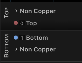
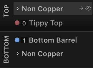
Notice that we get default names Top and Bottom for the copper layers. To customize this, we can add names for each of the Cu1oz instantiations:
    ...
    top_copper = Cu1oz(name="Tippy Top")
    core = FR4Core()
    bottom_copper = Cu1oz(name="Bottom Barrel")
    ...
Multi-layer Stackup#
In most modern designs, you will likely need more than 2 layers. If we were to build on the previous example to create a 4-layer board, it might look something like this:
class FR4Prepreg(Dielectric):
    thickness = 0.25 # mm

class Basic_Four_Layer(Stackup):
    top_solder_mask = LPIMask()
    top_copper = Cu1oz()
    pp1 = FR4Prepreg()
    gnd_copper = Cu1oz()
    core = FR4Core()
    vdd_copper = Cu1oz()
    pp2 = FR4Prepreg()
    bottom_copper = Cu1oz()
    bottom_solder_mask = LPIMask()
Similar structure to the 2-layer board with just more layers. Now if you imagine taking this to 6, 8, or more layers, this ends up being a lot of typing. We can take advantage of the symmetry present in most PCB stackups to reduce the amount of typing we need to do:
from jitx.stackup import Dielectric, Conductor, Symmetric

class Symmetric_Four_Layer(Symmetric):

  solder_mask = LPIMask()
  ext_copper = Cu1oz()
  pp = FR4Prepreg()
  inner_copper = Cu1oz()
  core = FR4Core()
This creates a 4-layer stackup with the same layer entries as Basic_Four_Layer.
Vias#
In JITX, each design can use a finite set of via types. We must define these via types in the Substrate class.
import jitx
from jitx.layerindex import Side
from jitx.via import Via, ViaType

class SampleSubstrate(jitx.Substrate):
  """Sample substrate using a two layer stackup and the sample fabrication
  constraints."""
  ...

  class MicroVia(Via):
    start_layer = 0
    stop_layer = 1
    diameter = 0.3
    hole_diameter = 0.1
    filled = True
    tented = Side.Top
    type = ViaType.LaserDrill

  class THVia(Via):
    start_layer = Side.Top
    stop_layer = Side.Bottom
    diameter = 0.45
    hole_diameter = 0.3
    type = ViaType.MechanicalDrill
Via Properties#
Each via definition supports several properties that control its manufacturing and behavior:
type — Specifies the drilling method:
ViaType.MechanicalDrill— Standard mechanical drilling. Used for through-hole vias and larger buried vias. Typical minimum hole diameter is around 0.2–0.3 mm.ViaType.LaserDrill— Laser-drilled microvias. Used for fine-pitch layer transitions (typically spanning 1–2 layers). Supports smaller hole diameters (down to ~0.075 mm) but is limited in the number of layers it can span.
filled — When True, the via hole is filled with conductive or non-conductive epoxy. Filled vias are required for via-in-pad designs where a component pad sits directly on top of the via. Without filling, solder can wick down through the hole during reflow, creating unreliable joints.
tented — Controls whether soldermask covers the via. Can be set to True (both sides), Side.Top, or Side.Bottom to tent specific sides. Tenting prevents solder from flowing into the via and protects against accidental shorts.
via_in_pad — When True, indicates the via is designed to be placed directly under a component pad. Typically used together with filled = True.
Here are examples illustrating common via configurations:
from jitx.via import Via, ViaType
from jitx.layerindex import Side

class THVia(Via):
    """Standard through-hole via — mechanically drilled, spanning all layers."""
    type = ViaType.MechanicalDrill
    start_layer = Side.Top
    stop_layer = Side.Bottom
    diameter = 0.45
    hole_diameter = 0.3

class FilledVia(Via):
    """Filled and tented via suitable for via-in-pad designs."""
    type = ViaType.MechanicalDrill
    start_layer = Side.Top
    stop_layer = Side.Bottom
    diameter = 0.45
    hole_diameter = 0.3
    filled = True
    tented = True
    via_in_pad = True

class MicroVia(Via):
    """Laser-drilled microvia spanning top two layers only."""
    type = ViaType.LaserDrill
    start_layer = 0
    stop_layer = 1
    diameter = 0.356
    hole_diameter = 0.178
    filled = True
    via_in_pad = True
In the above definitions, the Side.Top and Side.Bottom enumerated values resolve to 0 and -1 integer values, respectively.
To reference a via in code, we need to reference the substrate type by name:
class SomeCircuit(jitx.Circuit):
  def __init__(self):
    # Via Type
    viaType = SampleSubstrate.THVia
    # Instantiating the Via
    self.codePlacedVia = viaType().at(2.0, 3.0)
Via Structures#
When a signal transitions between layers of a PCB, a bare via on its own can introduce impedance discontinuities and crosstalk. A via structure wraps the signal via with surrounding ground vias (a “ground cage”), anti-pad keepout regions, and insertion point markers to create a controlled, well-shielded layer transition.
JITX provides via structure classes in the jitxlib.via_structures module. The key classes are:
SingleViaStructure — For single-ended signals.
DifferentialViaStructure — For differential pair signals.
A via structure is a Circuit with topology ports (sig_in, sig_out) and a COMMON (ground) port. You instantiate it and wire it into your circuit’s topology just like any other component.
Ground Cages#
A ground cage is a ring of vias surrounding the signal via to provide shielding. The PolarViaGroundCage class arranges ground vias in a circular pattern around the signal via.
PolarViaGroundCage is a dataclass — you create instances by passing arguments directly to the constructor:
from jitxlib.via_structures import PolarViaGroundCage

cage = PolarViaGroundCage(
    SampleSubstrate.THVia,  # via_def: which Via type to use for the cage vias
    count=12,               # total positions in the circular pattern
    radius=0.85,            # radius in mm from the signal via center
    skips=[0, 3, 6, 9],    # indices to leave empty (for trace routing escape)
)
The skips parameter is a list of indices (0-based, up to count - 1) indicating positions in the circular pattern where no via should be placed. This is how you create gaps for signal traces to enter and exit the structure.
Optional parameters:
theta— Starting angle in degrees (default0.0, pointing right along the X axis).pose— A Transform to offset the entire cage relative to the via structure origin.
.. note:: PolarViaGroundCage must be instantiated with its constructor arguments. Defining a subclass with class-level attributes will not work because the base class is a dataclass whose __init__ expects positional arguments.
Anti-Pads#
An anti-pad is a keepout region on internal copper layers that prevents the ground plane from shorting to the signal via. Use SimpleAntiPad to define one:
from jitx.layerindex import LayerSet
from jitx.shapes.composites import double_chipped_circle
from jitxlib.via_structures import SimpleAntiPad

antipad = SimpleAntiPad(
    double_chipped_circle(0.5, 0.4),     # keepout shape
    LayerSet.range(start=0, through=3),   # layers to apply to
)
The shape is placed as a KeepOut on the specified layers. The pose parameter (default identity) allows you to offset the anti-pad relative to the via structure origin.
Insertion Points#
Insertion points mark locations where the signal trace should connect to the via structure. They appear as custom layer decorations that guide manual placement adjustments. Use the convenience method to create a standard pair of insertion points above and below the via:
ins_pts = SingleViaStructure.create_std_insertion_points(0.8) # radius in mm
Single-Ended Via Structure#
A SingleViaStructure creates a shielded layer transition for a single-ended signal. It has three ports:
sig_in— Signal input (single Port)sig_out— Signal output (single Port)COMMON— Ground connection (single Port)
Here is a complete example showing how to instantiate a single-ended via structure and wire it into a topology between two components:
from jitx.circuit import Circuit
from jitx.layerindex import LayerSet
from jitx.net import Port
from jitx.sample import SampleSubstrate
from jitx.shapes.composites import double_chipped_circle
from jitxlib.via_structures import PolarViaGroundCage, SimpleAntiPad, SingleViaStructure

class MyCircuit(Circuit):
    # Define the via structure as a class attribute.
    # SampleSubstrate.MicroVia is the signal via definition.
    ssvia = SingleViaStructure(
        SampleSubstrate.MicroVia,
        ground_cages=[
            PolarViaGroundCage(
                SampleSubstrate.THVia,
                count=12,
                radius=0.85,
                skips=[0, 2, 3, 4, 6, 8, 9, 10],
            )
        ],
        antipads=[
            SimpleAntiPad(
                double_chipped_circle(0.5, 0.4),
                LayerSet.range(start=0, through=3),
            )
        ],
        insertion_points=SingleViaStructure.create_std_insertion_points(0.8),
    )

    def __init__(self):
        # Wire the via structure into the signal topology
        self.topo_in = self.comp1.pin >> self.ssvia.sig_in
        self.topo_out = self.ssvia.sig_out >> self.comp2.pin

        # Connect the ground cage to the ground net
        GND = self.comp1.gnd + self.comp2.gnd
        GND += self.ssvia.COMMON
The >> operator creates topology segments that flow through the via structure: comp1 → sig_in → [via] → sig_out → comp2. The COMMON port connects all the ground cage vias to your ground net.
Differential Via Structure#
A DifferentialViaStructure creates a shielded layer transition for a differential pair. It has the same three ports, but sig_in and sig_out are DiffPair ports instead of single ports. It also takes a pitch parameter specifying the distance between the P and N signal vias.
from jitx.net import DiffPair
from jitx.shapes.composites import double_notch_rectangle
from jitxlib.via_structures import DifferentialViaStructure, PolarViaGroundCage, SimpleAntiPad

class MyDiffCircuit(Circuit):
    diffvia = DifferentialViaStructure(
        SampleSubstrate.MicroVia,   # via definition (or a tuple of two for separate P/N vias)
        pitch=0.8,                  # distance between P and N vias in mm
        ground_cages=[
            PolarViaGroundCage(
                SampleSubstrate.THVia,
                count=12,
                radius=0.85,
                skips=[0, 2, 3, 4, 6, 8, 9, 10],
            )
        ],
        antipads=[
            SimpleAntiPad(
                double_notch_rectangle(1.5, 0.85, 0.45, 0.15),
                LayerSet.range(start=0, through=3),
            )
        ],
        insertion_points=DifferentialViaStructure.create_std_insertion_points(0.4),
    )

    def __init__(self):
        # Wire differential topology through the via structure
        self.topo_in = self.dp_in >> self.diffvia.sig_in
        self.topo_out = self.diffvia.sig_out >> self.dp_out

        # Ground cage connection
        GND = self.gnd_pin1 + self.gnd_pin2
        GND += self.diffvia.COMMON
If the P and N signals require different via definitions, pass a tuple:
diffvia = DifferentialViaStructure(
    (MySubstrate.MicroViaP, MySubstrate.MicroViaN),
    pitch=0.8,
    ground_cages=[...],
    antipads=[...],
    insertion_points=[...],
)
Multiple Via Structures#
For bus signals, you can create multiple via structure instances using a list comprehension:
class BusCircuit(Circuit):
    BUS_WIDTH = 4

    vias = [
        SingleViaStructure(
            SampleSubstrate.MicroVia,
            ground_cages=[
                PolarViaGroundCage(SampleSubstrate.THVia, count=12, radius=0.85, skips=[0, 6])
            ],
            antipads=[
                SimpleAntiPad(double_chipped_circle(0.5, 0.4), LayerSet.range(start=0, through=3))
            ],
            insertion_points=SingleViaStructure.create_std_insertion_points(0.8),
        )
        for _ in range(BUS_WIDTH)
    ]

    def __init__(self):
        GND = self.comp1.gnd + self.comp2.gnd
        self.topos = []
        for i in range(self.BUS_WIDTH):
            self.topos.append(self.comp1.pins[i] >> self.vias[i].sig_in)
            self.topos.append(self.vias[i].sig_out >> self.comp2.pins[i])
            GND += self.vias[i].COMMON