Pin Assignment#
One of JITX’s superpowers comes in the form of a feature we call “Pin Assignment.” The idea is to allow the user to define the different configurations of a particular component or circuit where the designer has options.
For example, in most microcontrollers (MCU), each IO pin can be mapped to a general-purpose IO (GPIO) register peripheral or to some other application specific peripheral like I2C, SPI, etc. Its common for the GPIO pins to be mapped into “Ports” consisting of 8, 16, 32, or some other number of pins. This gives the designer options when attempting to maximize the usage of the microcontroller. When designing a PCB in a traditional schematic capture tool, the designer is often forced to pick a single configuration. The additional options may be documented as annotations or not at all. This initial option may or may not be the optimal choice. The designer won’t necessarily know until he/she has done some work on the layout and routing. This can cause churn on the design as the right IO pin is selected for this application.
In JITX, we provide a way of encoding all of the available options as declarative statements. The physical design tool then enforces these options during layout and routing so that the best option can be chosen without churn.
For more details - reference the complete design example for this document.
Two Sides of the Problem#
The pin assignment provide typically consists of two entities:
Provides - These are the available port configurations that a given component or circuit can offer.
Requires - These are the demands made by some consumer who wants to acquire a port offer.
The Provides and Requires communicate their needs through a Bundle. A Bundle is a type derived from Port that demonstrates a signal mapping. For example:
class GPIO(Port):
  gpio = Port()

class DiffPair(Port):
  p = Port()
  n = Port()
Both GPIO and DiffPair are Bundles. The GPIO bundle has only a single signal. The DiffPair
bundle has two signals that can each be accessed individually. A Bundle can be hierarchically constructed
from Port instances or other Bundle instances.
These definitions can both be found in the jitx module - don’t recreate these yourself in your project.
GPIO Example#
Let’s continue with the GPIO example. If we consider the STM32H7, it has 8 ports, lettered A to H, with up to 16 controllable pins in each port. In JITX, we might define a component to look like this:
class STM32H7(jitx.Component):
    manufacturer = "STMicro"
    mpn = "STM32H7A3ZIT6"

    VDD = [Port() for _ in range(12)]
    VSS = [Port() for _ in range(13)]

    PA = [Port() for _ in range(16)]
    PB = [Port() for _ in range(16)]
    PC = [Port() for _ in range(16)]
    PD = [Port() for _ in range(16)]
    PE = [Port() for _ in range(16)]
    PF = {i: Port() for i in [6, 7, 8, 9, 10, 11, 14, 15]}
    PG = {i: Port() for i in [6, 7, 8, 9, 10, 11, 14]}
    PH = {i: Port() for i in [0, 1]}
Notice that I’ve organized the ports of the component to match the structure of the MCU. Ports F, G, and H don’t come with a full accountrement of pins - we only include a subset for those ports.
To provide a GPIO pin assignment for each of these ports, we need to first create a Circuit.
class MCU(jitx.Circuit):
    """STM32H7 Microcontroller Wrapper Circuit"""

    U = STM32H7()
Here we are defining a circuit that contains a single component U from the STM32H7 definition we used above. We need a circuit, because pin assignment problems can only be mapped to the Circuit object via the provide decorators.
To create the first set of GPIO pin assignments, we will use the @provide.all_of decorator:
class MCU(jitx.Circuit):
    """STM32H7 Microcontroller Wrapper Circuit"""

    U = STM32H7()

    @provide.all_of(GPIO)
    def PA_GPIO(self, b: GPIO):
        return [{b.gpio: p} for p in self.U.PA]
The provide.all_of decorator is a flag to indicate that the PA_GPIO method is special. There are typically no cases where you as the end user are going to call this PA_GPIO method. This is strictly about setting up the assignment problem. The PA_GPIO method is going to describe the JITX system what provide port offers are being made available by this circuit.
The PA_GPIO method has the typical self argument followed by one positional argument b:GPIO. The b parameter is not a circuit port in the traditional sense. It is a placeholder for mapping a port configuration. In this particular case, this mapping is trivial - it just has one pin.
The list comprehension over self.U.PA (Port A of the MCU) allows us to easily create one mapping offer per pin for Port A.
When the design for this circuit is run, the JITX system will compile all of the provide decorator marked methods and define the available provide offers for that circuit. In this particular case, we will see 16 GPIO offers available on this component.
What about the rest of the ports…#
There are obviously more GPIO pins on this microcontroller than just Port A. So to include all of them in the pin assignment problem, we need to incorporate Port B-H as well. The most naive way forward would be to just copy and paste our example and create PB_GPIO, PC_GPIO, etc methods with similar structures:
@provide(GPIO)
def PB_GPIO(self, b: GPIO):
    return [{b.gpio: p} for p in self.U.PB]

@provide(GPIO)
def PC_GPIO(self, b: GPIO):
    return [{b.gpio: p} for p in self.U.PC]
But that is very repetitive and tiresome. So let’s figure out a better way:
@provide.all_of(GPIO)
def P_GPIO(self, b: GPIO):
    ports = [
        self.U.PA,
        self.U.PB,
        self.U.PC,
        self.U.PD,
        self.U.PE,
        *[dictPort.values() for dictPort in [self.U.PF, self.U.PG, self.U.PH]],
    ]
    allGPIOs = [x for port in ports for x in port]
    return [{b.gpio: p} for p in allGPIOs]
With this approach, we collect up all of the port definitions and put them int the ports list. Note that for the port F, G, and H which are not fully populated - we need to handle them slightly differently by converting them from dict types to iterables using the values method.
Once we have each of the ports in a given form, we can use another list comprehension to flatten this list of iterators into a single list of Port instances. Then we use one final list comprehension (which should look very similar to what we did in PA_GPIO) to create the GPIO bundle mappings.
Pin Assignment in the Physical Design#
So if we now run this example, we can see the pin assignment configuration manifest in the layout. Select the GPIO in WP from the U2 component and press ctl + A. This will select the “Possible Ends” for the WP signal (outlined in green).
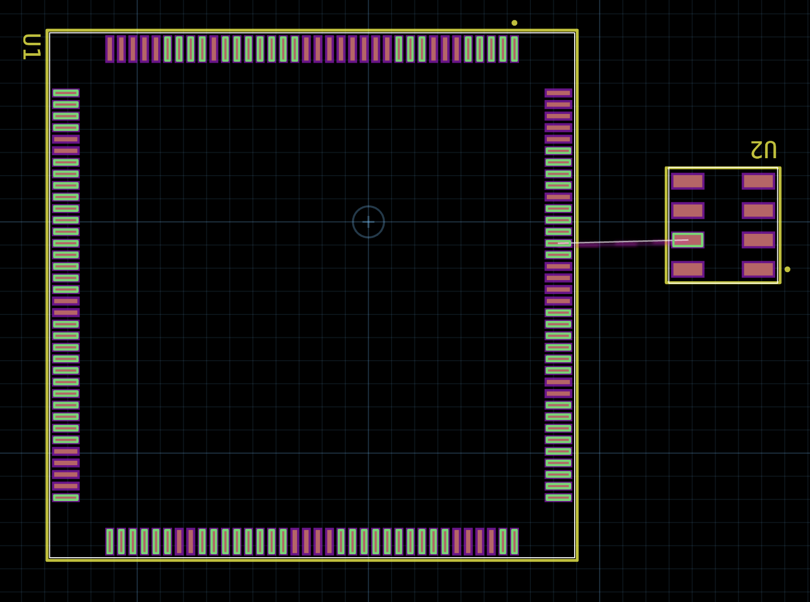
The possible ends of WP are the set of all pads that can satisfy the connection for WP. We can see that this WP pin can be connected to any valid GPIO on the microcontroller as we have defined them in code.
The “Rat’s Nest” line for the WP signal is showing a single possible end. This is a “Potential Solution” to the pin assignment problem for the WP signal. It doesn’t mean that WP must connect to only that pad. The primary purpose of the potential solution is to allow for the user to see one possible rat nest configuration for the circuit. The current heuristic is for this potential solution to use the pad that is closest to the WP pad as the crow flies.
It is a little subtle, but if you look close, you will notice that there is a slight purple color overlay for this rat’s nest line. This is an indication that this signal is participating in a pin assignment problem.
If we complete a route for WP by pressing q and then select WP and press ctl + A again:
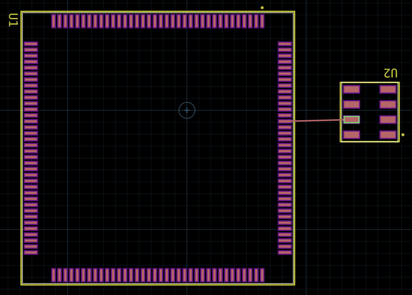
We will see the copper on the top layer connecting WP to the closest pad (in this case PB[4]) and we will see that there are no more possible ends for the WP signal. Since it has been routed, this is no longer a potential solution. We now have established an explicit solution for the WP signal. This signal and its endpoints no longer participate in the pin assignment solution. No matter what other pin assigned signals are present in the design, they will not be able to use PB[4] as a possible end.
Other provide variants#
There are two other provide decorator variants:
one_of- Given a set of N mappings, offer a single provider which can be fulfilled by any of the mappings.subset_of- Given a set of N mappings, offer M providers which can be fulfilled by any of the mappings (M < N).
For example, let’s say that we want to use a set of GPIO pins from the MCU as outputs. For each output we want to drive 5mA. In the datasheet for the STM32H7, it outlines that the max current sourced by all IO pins and control pins is 140mA. If we just ignore the control pins, then that would mean we can use a maximum of (140mA / 5mA) = 28 GPIO pins. To support this, we might use the following pin assignment setup:
@provide.subset_of(GPIO, 28)
def P_GPIO(self, b: GPIO):
    ports = [self.U.PA, self.U.PB, self.U.PC, self.U.PD, self.U.PE]
    allGPIOs = [x for port in ports for x in port]
With 5 ports, the provide.all_of(GPIO) would offer 16 * 5 = 80 total GPIO provide ports. By using provide.subset_of(GPIO, 28), this will limit the total offered provide ports to 28 options. Any of those 28 options can be selected from the 80 total GPIO pins.
Shortcut for all_of#
The @provide.all_of decorator can also be created using the shortcut @provide. For example, this:
@provide.all_of(GPIO)
def PA_GPIO(self, b: GPIO):
  ...
Is equivalent to:
@provide(GPIO)
def PA_GPIO(self, b: GPIO):
  ...
I2C Example#
For a more sophisticated example, we can look at a set of I2C peripherals on the STM32H7. In MCUs, it is common to have a pin multiplexer per IO pin. That multiplexer typically has a limited set of signals that can be piped through it to drive the output. This means that not all peripherals can drive every IO pin. If we consult the datasheet for the STM32H7 we see that for the I2C1 peripheral, there are the following options:
I2C1.SCLcan connect toPB6orPB8I2C1.SDAcan connect toPB7orPB9
To support a single I2C peripheral connection, we need to construct a hierarchical pin assignment problem:
First layer is the pin assignment problems for
SCLandSDASecond layer is the pin assignment problem for the
I2Cbundle consisting of the combinationsclandsda.
Here is an example of how we might do the first layer of the problem for the SCL pin:
class MCU(jitx.Circuit):
    """STM32H7 Microcontroller Wrapper Circuit"""

    U = STM32H7()

    class I2C1_SCL(Port):
        p = Port()

    @provide.one_of(I2C1_SCL)
    def I2C1_SCLs(self, b: I2C1_SCL):
        return [{b.p: p} for p in [self.U.PB[6], self.U.PB[8]]]
There are two things going on in this example:
We define an internal bundle type
I2C1_SCLthat is primarily intended to be used only inside theMCUcircuit class. This bundle type we are going to use to create a single provide offering for theSCLpin of theI2C1peripheral.Using the internal bundle type, we construct a single provide offering that can be satisfied by either
PB6orPB8.
We would do the same thing for I2C1.SDA using its associated ports PB7 and PB9. Duplicated here for completeness:
    class I2C1_SDA(Port):
        p = Port()

    @provide.one_of(I2C1_SDA)
    def I2C1_SDAs(self, b: I2C1_SDA):
        return [{b.p: p} for p in [self.U.PB[7], self.U.PB[9]]]
The second layer is combining these two internal providers to construct the I2C1 offering:
    @provide(I2C)
    def I2C1_Ports(self, b: I2C):
        sclProv = self.require(self.I2C1_SCL)
        sdaProv = self.require(self.I2C1_SDA)
        return [{b.scl: sclProv.p, b.sda: sdaProv.p}]
This state creates a single I2C provide port that selects from one of the options for each of the I2C1_SCL and I2C1_SDA offers. This results in a single port that could connect in one of the following 4 combinations:
Configuration #1:
I2C.scl => PB[6]
I2C.sda => PB[7]
Configuration #2:
I2C.scl => PB[6]
I2C.sda => PB[9]
Configuration #3:
I2C.scl => PB[8]
I2C.sda => PB[7]
Configuration #4:
I2C.scl => PB[8]
I2C.sda => PB[9]
Pin Assignment in Practice#
If we run the example design, we will see the following behavior in the physical design tool. I’ve selected either the SCL or SDA pins and pressed ctl + A to see all “possible ends.” In this case, the possible ends for SCL and SDA are much more limited than in the GPIO case.
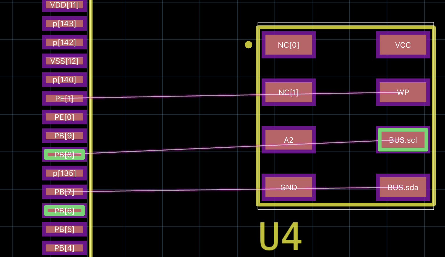
In this example - we see that both SCL and SDA have 2 possible ends. Notice that the sets for each match the code and the description above.
If we compare against the GPIO assignment to WP:
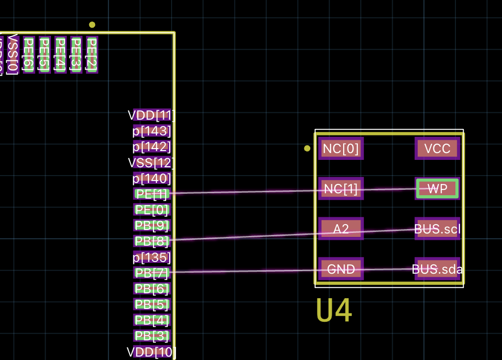
What you will notice is that the GPIO’s possible ends still includes the pads that can be assigned to SCL or SDA. This is the case because no explicit assignment has occurred yet. The assignment will only happen when a valid route connects the SCL and SDA pins.
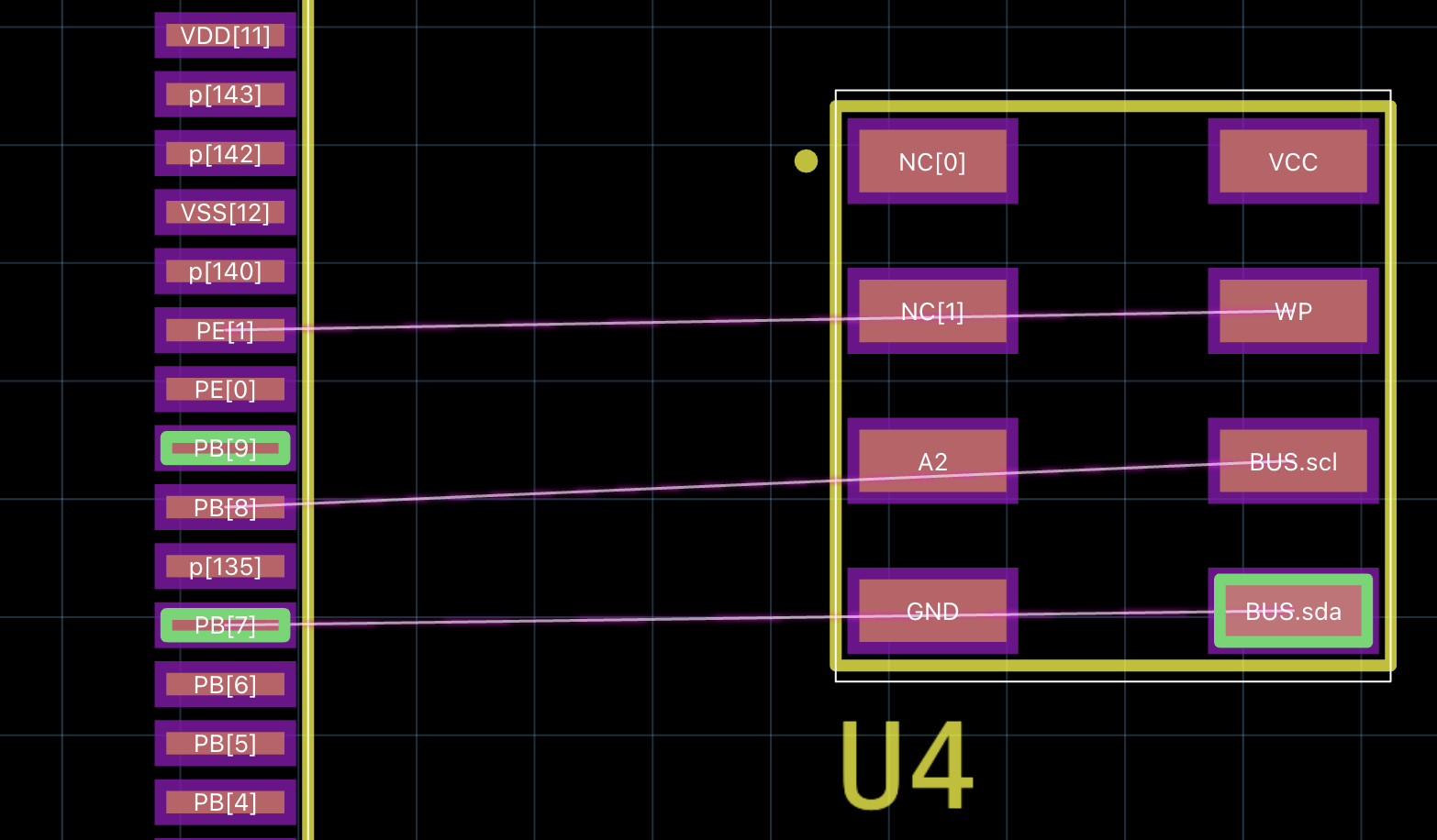
If we arbitrarily route the I2C signals between U2 and the MCU and then re-run ctl + A to see the possible ends for the WP signal - we will see:
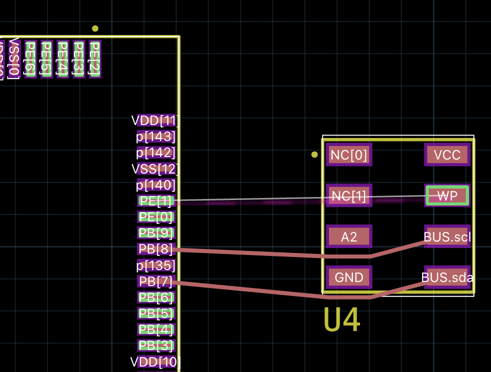
Notice that the pads for PB[7] and PB[8] are now no longer possible ends for the GPIO WP signal.