

Signal Integrity Constraints#
This is Part 1 of the Signal Integrity Essentials series. A signal integrity constraint puts a limit on a signal path: how long the signal may take to arrive, how much of it may be lost on the way, or how far apart two signals may arrive. In JITX we name a path by its two ends, the pad where the signal leaves and the pad where it arrives, and the constraint applies to everything between them. The connections along the way are the ordinary nets you already build with the + operator.
Naming a Signal Path#
Let’s start with a driver sending a signal through an AC coupling capacitor to a receiver. The circuit is two nets, one on each side of the capacitor, and one constraint that names the ends:
class Link(jitx.Circuit):
    def __init__(self):
        ...
        self.n1 = self.drv.o + self.cap.a
        self.n2 = self.cap.b + self.rcv.o

        self.cst = (
            Constrain(Topology(self.drv.o, self.rcv.o))
            .timing(1e-9)          # at most 1 ns from end to end
            .insertion_loss(3)     # at most 3 dB
            .structure(RS_50)      # a 50 ohm RoutingStructure
        )
A Topology only identifies a path by its begin and end ports. It doesn’t create any connection. The Constrain object collects the constraints for that path: timing and insertion_loss set limits on the whole path, and structure applies a RoutingStructure to the segments between the ends (Ends Inside Sub-Circuits shows a case where one segment misses it).
Notice that the Constrain object is assigned to self. Like everything else in a JITX circuit, a constraint is part of the design only when the circuit holds on to it.
The reports on this page come from circuits like these placed on the two-layer sample board, with RS_50 taken from its substrate, SampleSubstrate. Your own routing structure and stackup give different numbers.
JITX works out the path from drv.o to rcv.o on its own: along n1 to the capacitor, through the capacitor, and along n2 to the receiver. Two things have to be in place for that to work. The capacitor needs a pin model, and the nets need routes.
Parts the Signal Passes Through#
A net ends at a pad. For the path to continue on the far side of the capacitor, JITX needs to know that the signal passes through the part, and what that costs in delay and loss. A BridgingPinModel between the two ports says both:
class ACCap(jitx.Component):
    a = Port()
    b = Port()
    ...
    pin_model = BridgingPinModel(a, b, delay=5e-12, loss=0.1)  # seconds, dB
The model can also be added in the circuit, if the component you are using doesn’t already carry one. Give one to each part the signal passes through, such as an AC coupling capacitor or a series resistor. A shunt part, such as a termination resistor to ground, is not on the path between the ends and gets no BridgingPinModel.
If the capacitor has no pin model, the path stops at it, and the design issues say exactly where:
Topology:
  - No path for signal constraint from drv.o to rcv.o: the ends are only connected through the part between cap.a and cap.b, which has no pin model. If the signal is meant to pass through it, give it a pin model between them; otherwise check the wiring.
Pin Models at the Ends and on Vias#
An endpoint may provide a TerminatingPinModel. These models characterize the delay and loss from the silicon through the wire-bonding and out the package via its pins. In complex chips, this delay and loss may be different from one pin to another, so we add one model for each pad:
class Driver(jitx.Component):
    o = Port()
    ...
    o_model = TerminatingPinModel(o, delay=10e-12, loss=0.2)
The delay and loss values are typically found in the component datasheet under package parasitic or IBIS model specifications. These models are not strictly necessary. Without them, the endpoints add no delay or loss. With a 10 ps, 0.2 dB model on both ends of our example, the measured delay rises by 20 ps and the loss by 0.4 dB.
A via adds its own delay and loss when the path changes layers through it. Those come from the via definition’s models, one PinModel for each pair of layers the signal travels between:
class SignalVia(Via):
    ...
    models = {(0, 1): PinModel(delay=7e-12, loss=0.05)}  # layer 0 to layer 1
A via placed from code joins the net through a PortAttachment, and the path then counts its model for the layers its routes use:
        self.via = SignalVia().at(7, 0)
        self.via_attach = PortAttachment(self.cap.b, self.via)
Routes Close the Path#
JITX finds the path between the ends by following routed copper. Before the nets are routed there is nothing to follow, and so nothing to measure. Here is what the example reports with no routes:
Signal Constraint:
  - 2 issues: Unconnected Topology on Path: drv.o, cap.a
      - Unconnected Topology on Path: drv.o, cap.a
      - Unconnected Topology on Path: cap.b, rcv.o
  - 2 issues: Unconnected Topology on Path: drv.o, cap.a
      - Unconnected Topology on Path: drv.o, cap.a
      - Unconnected Topology on Path: cap.b, rcv.o
Routing:
  - Satisfied
The report has one group per constraint, here the timing limit and the loss limit, and each Unconnected Topology line in a group names a segment that has no route yet. You can route the nets in the board view, or from code with Route, which closes the path without opening the board view at all:
        self.routes = [
            Route(self.drv.o, self.cap.a, layer=0),
            Route(self.cap.b, self.rcv.o, layer=0),
        ]
A code Route is copper in your design, just like a route drawn in the board view, and it fixes how that connection runs on the board. Routes written only to check the constraints belong in a separate design: a subclass of your circuit that adds the routes, built as its own Design. That check design has its own placement and routes, so its numbers come from them, not from your board. The circuit you build the board from keeps its routing free, and its report shows the Unconnected Topology lines above until you route it. Whether the board meets each limit is read from the board’s own report once it is routed.
With the routes in place, the same report measures the constraints:
Signal Constraint:
  - Time: 170.785ps - Target: 500ps ± 500ps from drv.o to rcv.o
  - Loss: 0.665db - Target: 1.5db ± 1.5db from drv.o to rcv.o
Routing:
  - Satisfied
Notice that the target is written as a window, center and half-width: timing(1e-9) allows anything from 0 to 1 ns, which reads as 500ps ± 500ps. Notice also that the path runs from drv.o to rcv.o, across the capacitor. If the capacitor model were missing, this line would never appear. Checking Constraints with Design Issues shows how to get this report for your own design.
Ends Inside Sub-Circuits#
The ends can also be circuit ports. A circuit port stands in for the first pad behind it, the one component port it is joined to. When a sub-circuit wires its port straight to its chip, a constraint between two sub-circuits’ ports measures from chip to chip. When a circuit port reaches more than one pad, there is no single pad to stand in for, and the report says No path for signal constraint from a.p to b.p with no part named. Name the pad you mean instead.
A series part inside the sub-circuit is easier to miss. Here each sub-circuit puts an AC coupling capacitor, with its pin model, between its port and its chip, and every segment is routed:
class Endpoint(jitx.Circuit):
    p = Port()

    def __init__(self):
        ...
        self.n0 = self.p + self.ser.a
        self.n1 = self.ser.b + self.chip.o

class Link(jitx.Circuit):
    def __init__(self):
        ...
        self.n = self.a.p + self.b.p
        self.cst = Constrain(Topology(self.a.p, self.b.p)).timing(1e-9).structure(RS_50)
The constraint measures, and nothing in the report looks wrong:
Signal Constraint:
  - Time: 105.674ps - Target: 500ps ± 500ps from a.ser.a to b.ser.a
Routing:
  - Satisfied
Notice the ends in that line: a.ser.a and b.ser.a, the outer pads of the capacitors. Each port stood in for the first pad behind it, so the path stops at the capacitors. The segments from the capacitors to the chips carry neither the timing limit nor the routing structure. The figure shows the same effect on a differential pair through series resistors:
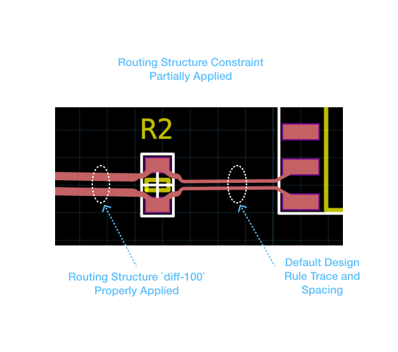
To constrain the whole path, name the chips’ pads as the ends:
self.cst = Constrain(Topology(self.a.chip.o, self.b.chip.o)).timing(1e-9).structure(RS_50)
The report now measures from chip to chip, with one more line:
Signal Constraint:
  - 2 issues: Missing routing structure on Path: a.ser.a, b.ser.a
      - Missing routing structure on Path: a.ser.a, b.ser.a
      - Time: 211.039ps - Target: 500ps ± 500ps from a.chip.o to b.chip.o
Routing:
  - Satisfied
The segment between the two capacitors, from a.ser.a to b.ser.a, did not get the structure. What sets it apart is that its net carries the sub-circuits’ ports. Joining that net at the capacitor pads, self.a.ser.a + self.b.ser.a, leaves the ports on it, and the report shows the same missing structure. Remove the ports from the sub-circuits, so that nothing but the two pads is on that net, and the one constraint covers the segment. A second constraint that names the ports puts the structure there without changing Endpoint:
self.mid = Constrain(Topology(self.a.p, self.b.p)).structure(RS_50)
With both constraints the Time from a.chip.o to b.chip.o drops, and nothing is missing. The delay changed because that segment is now computed with the routing structure. The exact numbers in this example can move by about 2 ps between runs, because the router can draw one of the short routes inside the sub-circuits differently: the one-constraint version has measured 211.039 ps and 213.255 ps, and the two-constraint version 182.253 ps and 184.468 ps. This isn’t optimal: whoever uses Endpoint has to know what is inside it.
Kinds of Constraints#
Constraints come in the form:
Medium Constraints - For example, RoutingStructure encodes the properties of the physical medium to create impedance-controlled single-ended geometry.
Medium Dependent Constraints - These constraints require a valid medium constraint (ie routing structure) to apply correctly.
TimingConstraint - These constraints encode the limits on the delay of the signal through the medium.
TimingDifferenceConstraint - These constraints encode the limits of the difference in signal delay between two signals.
InsertionLossConstraint - These constraints encode the limits on the loss of the signal through the medium.
Medium Constraints#
The medium constraints are primarily geometric constructs that define how a transmission line is formed in the PCB. These provide the broad class of controlled impedance constraints. In addition to geometry, these constraints will often provide necessary data to characterize the PCB transmission medium. These characteristics, like propagation speed, loss, etc, are used by other constraints.
The medium constraints primarily come in two forms:
RoutingStructure - Single-ended routing structure constraints
DifferentialRoutingStructure - differential pair routing structure constraints.
These constraints allow us to create:
Microstrips
Striplines
Edge-Coupled Striplines
And many others.
A constraint without a structure(...) still reports a number, but that number is not computed from your routing structure. Our first example measures 215.793 ps and 0.163 dB without RS_50, against 170.785 ps and 0.665 dB with it. The design issues add a Missing routing structure on Path: drv.o, cap.a line for each segment that has no structure, and each one is something to fix.
NeckDown & Structures#
Each type of medium constraint provides a NeckDown type, for example RoutingStructure.NeckDown or DifferentialRoutingStructure.NeckDown. The goal of neckdown is to provide an automated and constraint-based mechanism for the fan-out or fan-in of an impedance controlled signal. Oftentimes in BGAs or other space constrained packages, the terminations for impedance controlled signals may have narrow spacing. This may violate the typical clearance requirements that we want for our signal. The neckdown provides a way to specify the features of the trace in these areas of the board.
A neckdown is defined as part of a RoutingStructure.Layer or DifferentialRoutingStructure.Layer. It specifies reduced trace width and clearance values that the routing engine is allowed to use in constrained areas.
Single-Ended NeckDown#
from jitx.si import RoutingStructure, symmetric_routing_layers
from jitx.units import ohm
from jitxlib.physics import phase_velocity

vel = phase_velocity((4.4 + 1) / 2)  # microstrip effective Dk

RS_50 = RoutingStructure(
    impedance=50 * ohm,
    layers=symmetric_routing_layers({
        0: RoutingStructure.Layer(
            trace_width=0.12,
            clearance=0.2,
            velocity=vel,
            insertion_loss=0.018,
            neck_down=RoutingStructure.NeckDown(
                trace_width=0.09,   # reduced width in constrained areas
                clearance=0.075,    # reduced clearance in constrained areas
            ),
        )
    }),
)
Differential NeckDown#
For differential pairs, the neckdown also allows reduced pair_spacing. The uncoupled_region should have a matching neckdown for when the P and N traces separate:
from jitx.si import DifferentialRoutingStructure, RoutingStructure, symmetric_routing_layers
from jitx.units import ohm
from jitxlib.physics import phase_velocity

vel = phase_velocity((4.4 + 1) / 2)

DRS_100 = DifferentialRoutingStructure(
    impedance=100 * ohm,
    layers=symmetric_routing_layers({
        0: DifferentialRoutingStructure.Layer(
            trace_width=0.09,
            pair_spacing=0.137,
            clearance=0.2,
            velocity=vel,
            insertion_loss=0.018,
            neck_down=DifferentialRoutingStructure.NeckDown(
                trace_width=0.075,   # reduced trace width
                pair_spacing=0.1,    # reduced P-to-N spacing
                clearance=0.15,      # reduced clearance
            ),
        )
    }),
    uncoupled_region=RoutingStructure(
        impedance=50 * ohm,
        layers=symmetric_routing_layers({
            0: RoutingStructure.Layer(
                trace_width=0.09,
                clearance=0.2,
                velocity=vel,
                insertion_loss=0.018,
                neck_down=RoutingStructure.NeckDown(
                    trace_width=0.075,
                    clearance=0.15,
                ),
            )
        }),
    ),
)
The routing engine automatically activates the neckdown parameters when routing in areas where the standard trace width and clearance cannot be satisfied, such as BGA escape routing or dense connector fan-out regions.
Time-based Constraints#
Users familiar with legacy CAD systems will be familiar with the concepts of “Length Matching.” This is a very intuitive way to think about the propagation of signals. If the length of two signals are the same, then surely the propagation of the signals through the transmission line will be the same. This approximation leaves out of its analysis much of the nuance in high speed circuit design. The propagation delay for a signal through a particular medium is dependent on several factors. Transitioning from a top side microstrip to an internal stripline introduces yet more diversity in the propagation delay.
The problem with the length is that there isn’t really a way to modulate it given the physical characteristics of the medium. You could make arbitrary scaling factors on the length to account for things like vias, stripline vs microstrip, etc, but at the end of the day, these are all just fudge factors. There is no way to align these with the results from a simulation system like HFSS.
The routing structure constraints provide a mechanism to formulate the signal propagation delay for signals on different layers and through other structures. The routing engine can use this information to compute the delays or losses and then optimize the route geometry to meet the applied constraints.
TimingConstraint#
The TimingConstraint is a mechanism for explicitly controlling the delay of a given signal.
A signal propagates from the source to the destination, starting at time t0 and arriving at the receiver at t1. The delay for the signal is t1 - t0. This constraint type sets the limits for this delay.
This functionality is not super common but is useful for many RF applications - like phased array antennas.
  def __init__(self):
    ...

    phase_delay = Toleranced(1.0e-9, 10.0e-12) # 1nS +/- 10pS
    self.phaseCst = Constrain(Topology(self.elem[0].sig, self.elem[1].sig)).timing(phase_delay)
In this example, we establish an element to element phase delay of 1.0ns ± 10ps. The Constrain object identifies the endpoints of the topology we are attempting to apply a constraint to. The timing method applies a particular type of constraint, in this case a TimingConstraint to this topology. These endpoints typically resolve to the pads of the component (in this case, the feed pad of the patch antenna element).
Once the trace with a timing constraint is realized, the constraint will force the routing engine to continuously evaluate the characteristics of the trace. You will see a message in the “Issues List” under “Unsatisfied Signal Constraints”:
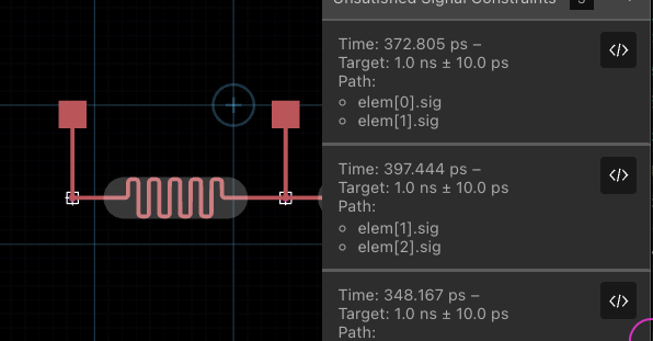
The “Time” meaning the current delay of the signal as calculated by the routing engine.
The “Target” meaning the actual constraint we’re trying to achieve, in this case
1.0ns ± 10ps.The “Path” meaning the endpoints that identify the path on the topology where this constraint is applied.
The shaded section is a “Signal Tuning” section (previously called the “Length Matching” section). Inside this section, the routing engine attempts to match the tuning parameters, primarily delay and loss, to meet the constraint requirements. In the above example, the signal tuning section is too small. So the routing engine makes its best effort and packs the signal tuning section with as many squiggle periods as it can. It then creates the “Unsatisfied Signal Constraint” issue in the issues list.
If the signal tuning section is large enough, the routing engine will typically optimize the length of the trace with variable pitch and amplitude of the “squiggle.” Here are some examples of how the routing engine might create this trace in this case:
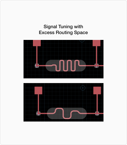
In this example, I’ve changed the signal propagation speed to slow down the signal artificially. This allows the routing engine some breathing room to demonstrate the above cases.
Notice that the period of squiggle changes and eventually the amplitude. The size of the signal tuning region defines the maximum amplitude of the signal. Currently, the other parameters of the squiggle like minimum turn radius, minimum period, and shape are not controllable by the user, but these will come in the future.
When the signal successfully achieves the timing constraint - the “Unsatisfied Signal Constraint” issue will disappear from the list. This is an actively assessed condition and changes in the board may cause it to re-appear.
Timing Difference Constraint#
The TimingDifferenceConstraint introduces a mechanism for controlling the timing skew between two signals.
Two signals propagate down a transmission line and at the end there is a time difference or skew between the two signals (shown below as ∆T):
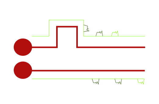
This is a very common constraint in a wide variety of applications:
Differential Pairs
Intra-pair skew - ie, P to N.
Inter-pair skew - for example, in MIPI-CSI for CLK and DATA diff-pair lanes.
Parallel Data Buses
Bus Member to Member
Bus Members to Strobe, for example in DDR memory
For “intra-pair” skew, the timing difference constraint drives the routing engine to use deskew bumps in the “Signal Tuning” regions. These “deskew bumps” attempt to achieve a phase matched relationship between the p and n signals of a differential pair.
  def __init__(self):
    ...
    skew = Toleranced(0.0, 1.0e-12)
    self.skewCst = ConstrainDiffPair(
      Topology(self.MCU.MIPI.CLK, self.IMGR.MIPI.CLK) # DiffPair endpoints
    ).timing_difference(skew)
The ConstrainDiffPair object captures the endpoint of the topology to which we can then apply one or more constraints. In this case, we add only one constraint via the timing_difference method. This method adds a TimingDifferenceConstraint object to our circuit.
Note how the ConstrainDiffPair object is assigned to a class definition using self.skewCst = .... We will see another pattern for this when we introduce the SignalConstraint types.
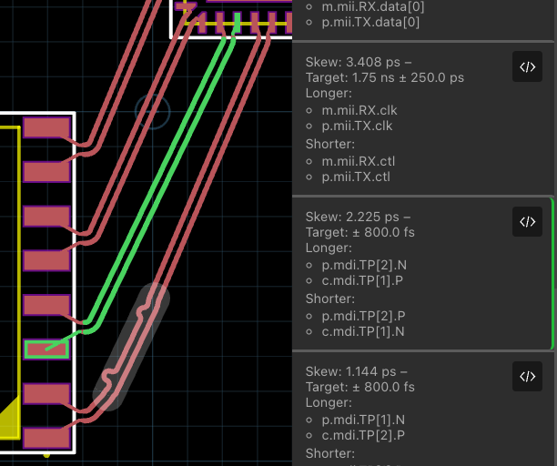
In the image above we can see multiple differential pairs routed in a circuit. The “Issues List” on the left shows the current set of “Unsatisfied Signal Constraints.” In this case, we have selected the first intra-pair skew constraint that is unsatisfied. The board view shows the associated traces highlighted in the board view. It is displaying for useful information for diagnosing and resolving this constraint:
The
Skewis the current total skew between the signals in thisdiff-pairbundle signal.The
Targetis the constraint specified in code. In this case we’re targeting0.0 ± 800.0 fs(femtoseconds).This constraint is likely more restrictive than you will see in practice.
We’ve exaggerated this constraint to make it easier to demonstrate this matching condition in JITX.
LongerandShorterrefer to the delay of the compared signal topologies by endpoint.In this particular example, the PHY side allows for swapping
PandNin the diff-pair.Hovering over the longer or shorter endpoints will highlight those routes on the board.
Beside that differential pair is another differential pair with a signal tuning section applied to it. Notice in that in this signal tuning section, the routing engine has applied two deskewing bumps of different sizes. Notice that the maximum amplitude of the deskew bumps is defined by the signal tuning sections envelope and a hard-coded maximum bump amplitude. The routing engine constructs these deskew bumps to remove the skew between the p and n signals per the user’s constraints.
Deskew Bump Features#
Creating useful deskew bumps is a complex task. There are many knobs and features to tweak to get a reasonable circuit representation. The following section is going to outline some of these features. Keep in mind that in the current implementation, many of these features are hard-coded. Future JITX versions will make more of these features accessible for configuration.
Deskew Bump Amplitude#
As described above, the amplitude for the deskew bumps is defined by the envelope of the signal tuning region. But depending on conditions, the routing engine will attempt to maximize what area it has available to it.
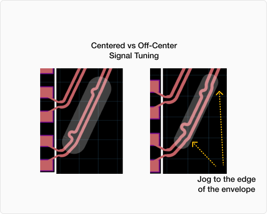
In the example above, if we oversize the envelope, then the differential pair will center itself to take the shortest path. If the envelope is too small, then the router will attempt to shove the differential pair as far to one side as it can in order to maximize the deskew bump amplitude.
Deskew Bump Spacing#
Notice that the deskew bumps are spaced according to the size of the envelope. In addition, the algorithm is currently hard coded with a maximum space between deskew bumps within a given envelope.
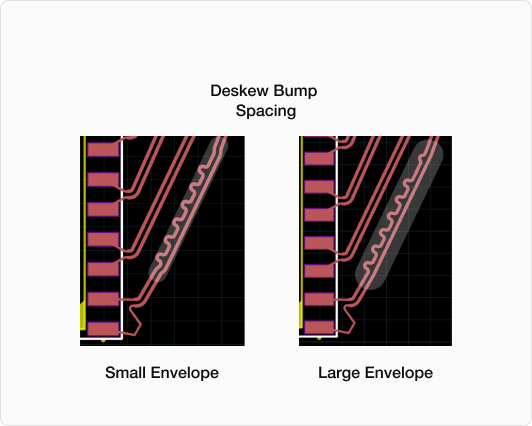
Skew Across a Bundle#
Skew between pairs, such as the lanes of a link that must arrive together, uses ConstrainReferenceDifference. It compares each path in a list against one guide path. The guide has to be a single pin, not a whole differential pair, so for a bundle of pairs we pick one leg as the guide:
  def __init__(self):
    ...
    t1 = Topology(self.drv.tx, self.conn.tx)
    t2 = Topology(self.drv.tx2, self.conn.tx2)
    self.skew = ConstrainDiffPair([t1, t2]).timing_difference(1e-12).timing(1e-9).structure(DRS_100)
    self.bundle = ConstrainReferenceDifference(
        Topology(self.drv.tx.p, self.conn.tx.p),  # the guide: one leg of the first pair
        [Topology(self.drv.tx2.p, self.conn.tx2.p), Topology(self.drv.tx2.n, self.conn.tx2.n)],
    ).timing_difference(2e-12)
Here each of the two pairs runs through AC coupling capacitors with bridging pin models, and the nets are routed. ConstrainDiffPair takes a list of pair topologies, so one object holds the intra-pair skew, timing and structure for both pairs. The reference difference holds both legs of the second pair to within 2 ps of the guide. The report shows every measurement:
Signal Constraint:
  - Time: 170.672ps - Target: 500ps ± 500ps from drv.tx.p to conn.tx.p
  - Time: 169.59ps - Target: 500ps ± 500ps from drv.tx.n to conn.tx.n
  - Time: 169.225ps - Target: 500ps ± 500ps from drv.tx2.p to conn.tx2.p
  - Time: 169.59ps - Target: 500ps ± 500ps from drv.tx2.n to conn.tx2.n
  - Skew: 1.082ps - Target: ± 1ps (longer from drv.tx.p to conn.tx.p, shorter from drv.tx.n to conn.tx.n)
  - Skew: 365.495fs - Target: ± 1ps (longer from drv.tx2.n to conn.tx2.n, shorter from drv.tx2.p to conn.tx2.p)
  - Skew: 1.447ps - Target: ± 2ps (longer from drv.tx.p to conn.tx.p, shorter from drv.tx2.p to conn.tx2.p)
  - Skew: 1.082ps - Target: ± 2ps (longer from drv.tx.p to conn.tx.p, shorter from drv.tx2.n to conn.tx2.n)
Routing:
  - Satisfied
The first two skew lines are the intra-pair constraints, one per pair. Notice that the first pair is outside its target: 1.082 ps against ± 1 ps. Nothing in its line says so; its group’s satisfied is False (Checking Constraints with Design Issues shows how to read it). The last two are the bundle constraint, each leg of the second pair against the guide.
The printed Target also drops the sign of the window. ConstrainReferenceDifference checks the guide’s delay minus each target’s delay against the window you give, and a window of -1 ns to 0 prints as Target: 500ps ± 500ps, the same as 0 to 1 ns. Read group.satisfied for pass or fail against the window as you wrote it, rather than the Target.
Power-based Constraints#
A common first order approximation of loss is the length of the signal. Like with time vs length, this approximation doesn’t take into account many of the non-obvious features of a board. The routing engine uses loss as a metric so that we can implement features similar to a channel operating margin analysis.
Insertion Loss Constraint#
The InsertionLossConstraint provides a mechanism to enforce limits on signal loss. It is common for protocols like USB, PCIe, etc to limit the acceptable insertion loss presented by the PCB.
The most typical application of an insertion loss constraint is to implement a maximum loss restriction on the signal. This constraint depends on a valid routing structure that provides an accurate insertion loss rate for each layer and structure. Without accurate data, this constraint won’t be successfully computed.
  def __init__(self):
    ...

    max_loss = Toleranced.min_max(0.0, 12.0)
    self.lossCst = Constrain(
      Topology(self.MCU.uSD.CLK, self.conn.uSD.CLK)
    ).insertion_loss(max_loss)
The insertion_loss method specifies loss in dB at the frequency of interest. Note that the insertion_loss of the RoutingStructure is assumed to be in dB/mm at this same frequency of interest.
Checking Constraints with Design Issues#
Every report on this page comes from the design issues, which you read from Python. Run a script like this from your project’s root, with the JITX runtime for your project running (if none is, jitx runtime start --background starts one):
import jitx

from myboard.main import MyDesign


def main() -> None:
    with jitx.runtime as rt:
        report = rt.submit(MyDesign).issues(satisfied=True, wait=30)
        if not report.complete:
            print("report incomplete: raise wait and run again")
        for group in report.groups():
            print("met" if group.satisfied else "NOT MET", group.text)
            if len(group.issues) > 1:
                for issue in group:
                    print("   ", issue.text)


if __name__ == "__main__":
    main()
The check sits in main() behind the __name__ test because JITX imports the Python files in your project when it looks for designs, and the guard keeps that import from running the check. submit loads the design into the runtime, and its issues method returns an IssueReport. These come from jitx.run and jitx.issue, which are still marked experimental and may change. Each IssueGroup in the report holds the result of one check, such as one constraint. A group’s text shows only its first issue when it has several, as in 2 issues: Missing routing structure on Path: ..., so the inner loop prints each issue. For the routed example from earlier, the script prints:
met Time: 170.785ps - Target: 500ps ± 500ps from drv.o to rcv.o
met Loss: 0.665db - Target: 1.5db ± 1.5db from drv.o to rcv.o
met Satisfied
The last line is the Routing category’s one group, which reports that routing is satisfied. The other reports on this page are print(report.text()), which prints each group’s text under its category name and, for a group of several issues, each issue below it.
The satisfied=True argument matters here. Without it, the report lists only what is wrong, and a constraint that is met doesn’t appear at all. For our routed example, report.text() then reads:
No design issues.
That reads like good news, but it is the same report you would get from a constraint the design never applied. So we treat a constraint with a timing, loss or skew limit as applied only when its group carries a measurement: a Time, Loss or Skew value naming the two ends. The measurement can sit in any issue of the group. In the sub-circuit example, the Time is the second issue of a group whose text names the missing structure.
Whether that measurement meets the limit is a separate question, and only group.satisfied answers it. The text reads the same for a met constraint and a missed one, as the bundle example shows.
A constraint that carries only a routing structure, such as self.mid in Ends Inside Sub-Circuits, has nothing to measure, so it never appears in the report, met or not. For that one, the constraint in your code is what you check, together with the timing or loss constraint over the same path: once that one measures, no Missing routing structure line should name the segments the structure covers.
wait=30 gives the runtime up to 30 seconds to finish its checks before the report is taken; the default is 5. A category still running when the wait ends comes back pending, and the report’s complete property is False. Check complete before you trust a short report: report.text() leaves out a category that has no groups yet, so it can print No design issues. while checks are still running. For a pass or fail over the whole design, bool(report) is True when the report holds any error, and report.errors lists them.
When a measurement is missing, the report usually says why. These are the messages we have met on this page, and what each one asks for:
Unconnected Topology on Path: drv.o, cap.ameans that segment has no route yet. Route it in the board view or from code.Signal path from drv.o to l1.o is not routed yet: ...can appear when the ends sit on one net of three or more pads and no routes join them. Route the net.No path for signal constraint from drv.o to rcv.o: ...followed by a part name means that part has no pin model. Add aBridgingPinModelif the signal passes through it. With no part named, JITX found no single path between the ends. Check that each end is one pad rather than a circuit port that reaches several, and that the nets between them are routed.Missing routing structure on Path: ...names a segment the constraint gave no routing structure, and the measurement beside it is not computed from your structure.Unassigned Pin on Path: ...means a pin assignment on the path hasn’t resolved yet. The next section covers this case.Code route dropped: it conflicts with other connections, underRouting, means JITX discarded one of your code routes, for example one that matches no offered pin mapping. The path it was meant to close stays open.
Constraints on Pin-Assigned Ports#
The ends of a path can be ports that come from Pin Assignment. Here a sub-circuit holds a part u with two physical pairs, a and b, and offers one differential pair in three ways: pair a, pair b, or pair a with p and n swapped:
class Src(jitx.Circuit):
    def __init__(self):
        self.u = TwoPairPart()

    @provide.one_of(DiffPair)
    def lane(self, dp: DiffPair):
        u = self.u
        return [
            {dp.p: u.a.p, dp.n: u.a.n},  # pair a
            {dp.p: u.b.p, dp.n: u.b.n},  # pair b
            {dp.p: u.a.n, dp.n: u.a.p},  # pair a, inverted
        ]
The circuit that uses it, as self.src = Src(), constrains the port that require() returns:
  def __init__(self):
    ...
    req = self.src.require(DiffPair)
    self.nets = [req.p + self.conn.tx.p, req.n + self.conn.tx.n]
    self.cst = (
        ConstrainDiffPair(Topology(req, self.conn.tx))
        .timing_difference(1e-12)
        .timing(1e-9)
        .structure(DRS_100)
    )
Notice that req is a local variable. A required port can’t be stored on self: the build fails with an error saying it should not be a member field of a circuit.
Until JITX knows which physical pins req lands on, there is no path to measure:
Signal Constraint:
  - Unassigned Pin on Path: nets[0].p
  - Unassigned Pin on Path: nets[0].n
  - 2 issues: Unassigned Pin on Path: nets[0].p
      - Unassigned Pin on Path: nets[0].p
      - Unassigned Pin on Path: nets[0].n
Routing:
  - Satisfied
Routes resolve the assignment. A route can’t end on a required port (the build fails with Using require ports as route ends at circuit.r[0] is not implemented), so we route the physical pins of u inside src:
    u = self.src.u
    self.r = [
        Route(u.a.p, self.conn.tx.p, layer=0),
        Route(u.a.n, self.conn.tx.n, layer=0),
    ]
JITX matches the routes to the first mapping, pair a, and the constraint measures from src.u.a.p to conn.tx.p. Routing u.a.n to conn.tx.p and u.a.p to conn.tx.n instead picks the third mapping, pair a inverted. Routes that match no offered mapping, such as u.b.p to conn.tx.p with u.a.n to conn.tx.n, are not all accepted: the report says Code route dropped: it conflicts with other connections, the p side stays unassigned, and only the n side measures.
Because the routes pick the mapping, a design that carries them has given up its pin-assignment freedom: of the three ways Src offers the pair, the board can use only the one the routes match. Keep routes like these in the separate design you build to check the constraints, as in Routes Close the Path. Its measurements are for that one mapping and its check routes, not for the board. The circuit you build the board from leaves req unrouted, so its report shows the Unassigned Pin lines above, and it keeps all three mappings open.
Daisy Chains#
Everything on this page uses plain nets, because naming the two ends is enough for JITX to find the path. One case asks for more: a daisy chain such as a DDR flyby clock or address bus, where the connection must visit its loads in a fixed order. Daisy-Chain Topologies covers how to state that order.
In the next section, we’re going to introduce higher level functions that use the topology and constraint primitives for effective modular designs.