

Layout Constraints#
Layout constraints are the design constraints that set a board’s copper. We
write each one with design_constraint.
A rule pairs a condition with an
effect. The condition is made of tags, labels
we put on objects to mark them as a power net, a small pad or a pour. The
effect sets what every object with those tags gets: a trace width, a narrower
fanout width at a fine-pitch pad, a clearance from other copper or the board
edge, a thermal relief, stitching vias, a via fence.
JITX applies the rules while it builds the layout, so they shape the copper as it is made: the router moves a trace to keep its clearance, and a pour is cut back around other-net copper.
Defaults above the fab floor#
Under every rule sits the substrate. Its
FabricationConstraints hold the
fabricator’s minimums, such as min_copper_width and min_copper_edge_space,
and where no rule sets a value, copper comes out at that floor. On the
SampleSubstrate, we get a 0.127 mm route
wherever no width rule matches.
Set a few defaults above the floor, and raise the power nets above them with
rules on their tag. On a
SampleDesign, which
brings the sample board and substrate:
class MyDesign(SampleDesign):
    circuit = MyCircuit()

    def __init__(self):
        self.rules = [
            design_constraint(IsTrace).trace_width(0.2),
            design_constraint(IsCopper, IsCopper).clearance(0.2),
            design_constraint(IsPad).thermal_relief(0.25, 0.25, 4),
            design_constraint(PowerTag(), priority=2).trace_width(0.5),
            design_constraint(PowerTag(), AnyObject, priority=2).clearance(0.3),
        ]
The first three are the defaults: a
trace_width for every
trace, a clearance
between any two pieces of IsCopper, and a
thermal_relief for
every pad. The last two give power nets a wider trace and more room from
AnyObject.
At priority 2 the PowerTag() width rule beats the IsTrace default, which
would win at equal priority by
specificity.
When we build this design, the SIG route comes out 0.2 mm wide with the pour 0.21 mm from it, and the VCC route 0.5 mm wide with the pour 0.31 mm away. Notice that against a trace or the board edge, a pour stops about 0.01 mm beyond the clearance.
We also get four 0.25 mm spokes across a 0.25 mm gap between each GND pad and the pour. A pad that no relief rule matches joins its pour solid, which is why we make the relief rule a default.
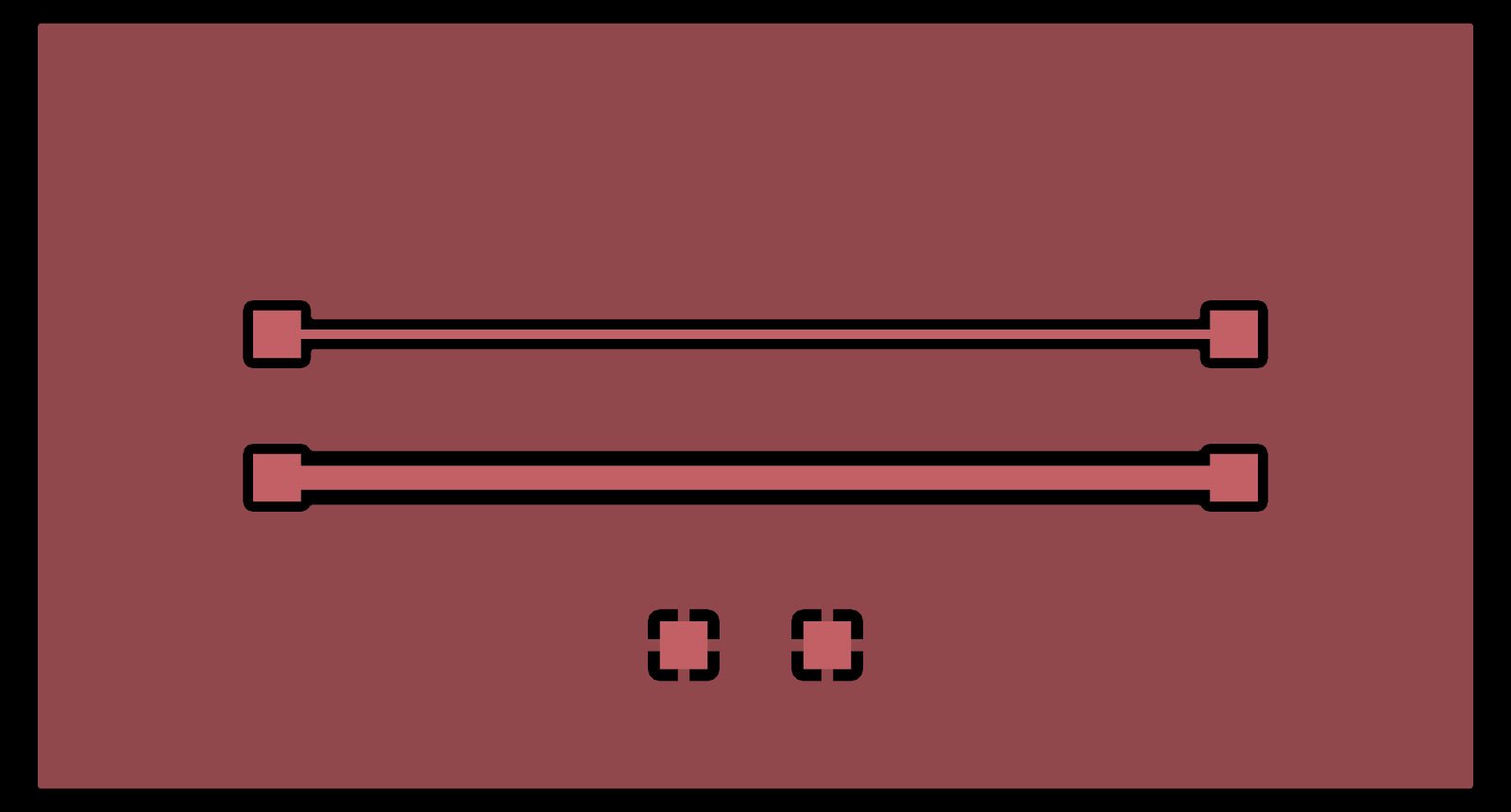
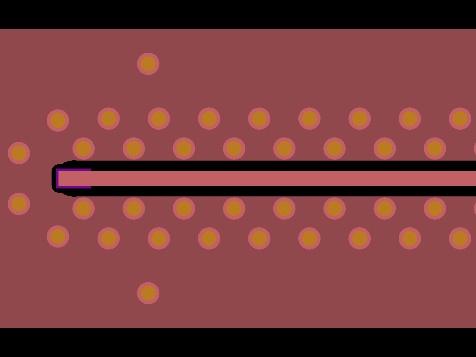
In the image above, notice the gaps along the narrow SIG route at the top and
the wide VCC route below it and around their end pads, and the spokes joining
each GND pad to the pour. The full design is
layout_default_rules,
which passes its rules through
check_against_fab
to raise an error if a width, clearance, relief gap or relief spoke is under
the substrate’s floor.
These rules size the copper JITX builds. A copper shape placed from code with
Copper can break a rule, and it reaches the layout as
written (Copper Shapes, Net Ties and Virtual
Connections).
Fanout from fine-pitch parts#
On a board whose power nets need 0.8 mm, wider than the pads they reach, the trace has to step down for the last stretch. A 0.8 mm trace centered on a 0.17 mm QFN pad at 0.5 mm pitch comes within 0.015 mm of the neighboring pads, under the 0.127 mm floor.
The QFN and derive_escape below come from the jitxexamples package, as do
the helpers in later examples, so to run them, add jitxexamples to the
project’s dependencies. The PowerTag rule still sets the net’s width, and
we make the last stretch a route of its own, with a tag and a higher-priority
rule. Here the two rules are circuit attributes, which apply to the whole board
as entries in self.rules do:
class QfnEscapeTag(Tag):
    """Escape segments into a QFN pad."""

class QfnPowerEscape(Circuit):
    def __init__(self):
        # PlaceholderQfn16 is the 16-lead, 0.5 mm pitch QFN of layout_qfn_escape,
        # at the origin so u1's landpattern frame is the circuit's frame
        self.u1 = PlaceholderQfn16().at(0, 0)
        ...   # a power source and the VDD net
        fab = jitx.current.substrate.constraints
        geo = derive_escape(
            self.u1.landpattern, self.u1.landpattern.p[1], fab,
            escape_clearance=fab.min_copper_copper_space,
        )
        self.transition = RoutePoint(layer=0).at(*geo.transition)
        self.vdd += self.transition.port
        PowerTag().assign(self.vdd)

        self.trunk = Route(self.source.out, self.transition.pad, layer=0)
        self.escape = Route(self.transition.pad, self.u1.VDD, layer=0)
        QfnEscapeTag().assign(self.escape)

        self.power_rule = design_constraint(PowerTag(), priority=2).trace_width(0.8)
        self.escape_rule = design_constraint(QfnEscapeTag(), priority=4).trace_width(
            geo.width
        )
The trunk and the escape meet at a RoutePoint
1.0 mm outside the pad. Both width rules match the escape and priority 4 wins
there, while the trunk keeps 0.8 mm.
derive_escape, from
layout_qfn_escape, takes the
clearance the escape keeps to the other pads, and reads the escape width from the placed pads:
narrower than the pad, and narrow enough to keep that clearance. For this
0.17 mm pad it is 0.15 mm, which leaves 0.34 mm to each neighbor. This board
sets no clearance rule, so we pass the fab floor. On a board that does, pass
the clearance that governs the net.
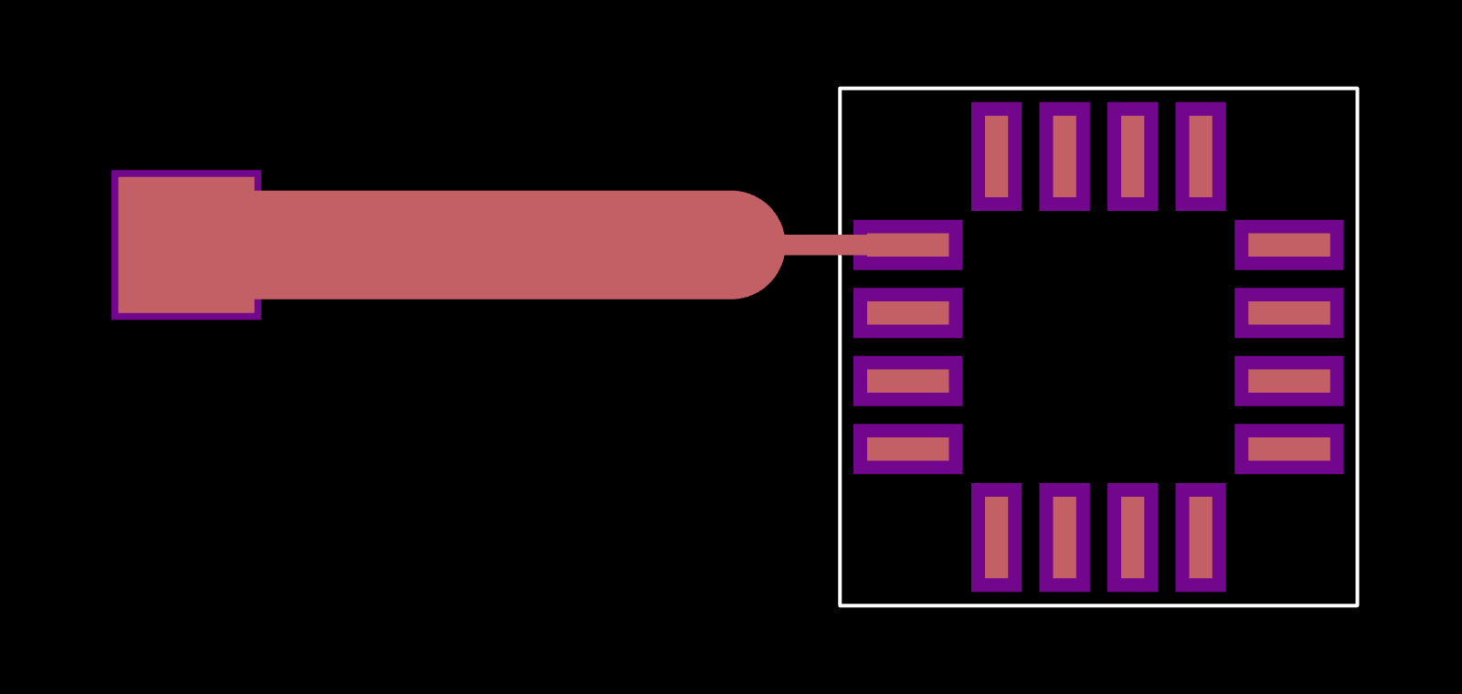
In the image above, notice the step in width at the route point, where the narrow escape leaves the trunk and runs into the top pad of the QFN’s left row.
A BGA ball
(layout_bga_escape) and a
differential pair
(layout_diff_pair_escape)
step down the same way, with rules on tags on their escape routes.
Routing structures by tag#
A
routing_structure
rule applies a RoutingStructure to whatever its
tag matches, the way the PowerTag rule applies a width, so a net can take its
structure with no .structure(...) on its
topology.
Here a rule on the net’s tag gives the line its main structure, and a second
rule, on a tag on the escape route, gives that segment a neck. The two tags,
SignalTag and EscapeNeckTag, are plain Tag subclasses from
layout_routing_structure_by_tag:
def line_structure(name: str, width: float) -> RoutingStructure:
    layer = RoutingStructure.Layer(
        trace_width=width, clearance=0.2, velocity=150e9, insertion_loss=0.01
    )
    return RoutingStructure({0: layer}, impedance=50, name=name)

class NeckedLine(Circuit):
    def __init__(self):
        ...   # two parts, the SIG and GND nets, the transition via, the tags
        self.main = line_structure("MAIN", 0.3)
        self.neck = line_structure("NECK", 0.15)
        SignalTag().assign(self.sig)
        self.escape = Route(self.device.io, self.transition, layer=0)   # pad to via
        self.run = Route(self.transition, self.far.io, layer=0)
        EscapeNeckTag().assign(self.escape)
        self.timing = Constrain(Topology(self.device.io, self.far.io)).timing(1e-9)

        on_net = design_constraint(SignalTag(), priority=2)
        on_escape = design_constraint(EscapeNeckTag(), priority=4)
        self.main_rule = on_net.routing_structure(self.main, ref_net=self.gnd)
        self.neck_rule = on_escape.routing_structure(self.neck, ref_net=self.gnd)
The escape comes out 0.15 mm wide and the main segment 0.3 mm. The timing
constraint on the path, a Constrain, requires a
structure on every segment, and with both rules in place the issues list shows no
Missing routing structure.
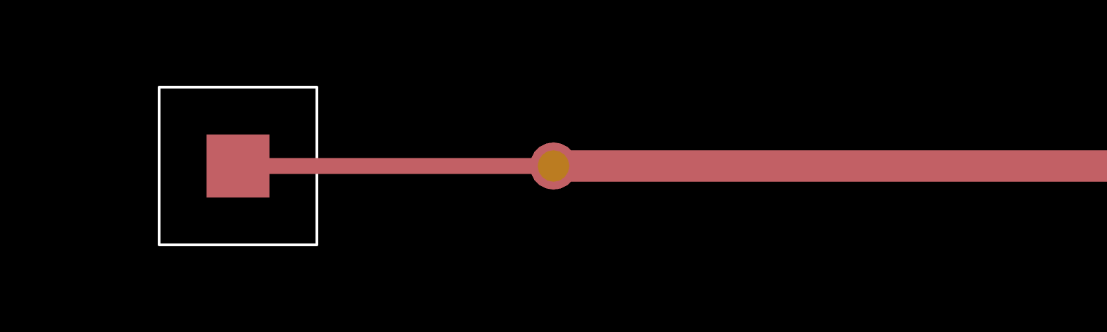
In the image above, notice the narrow escape from the device pad, inside its courtyard outline, to the transition via, and the wider main segment leaving the via to the right.
Put the neck tag on the Route; keyed on the net’s tag, the rule necks the
whole net. If a Constrain with .structure(...) and a rule both apply a
structure to one net, the rule wins with no issue.
Build structures inside a circuit’s __init__ or as class attributes of a
Substrate: one built at module level fails
with TypeError: 'Instantiable' object is not iterable. The whole design is
layout_routing_structure_by_tag.
Stitching a pour#
A stitch_via rule keyed
on a pour tag fills every pour that carries the tag with vias on a grid. The
vias take the pour’s net, and you place none of them by hand:
class StitchedPourTag(Tag):
    """Pours filled with stitch vias."""

class StitchedPour(Circuit):
    def __init__(self):
        ...   # the GND net, a GND plane on layer 1, a SIG route across its top
        self.gnd_pour = Pour(rectangle(12, 9).at(2.3, 1.1), layer=0)
        StitchedPourTag().assign(self.gnd_pour)
        self.GND += self.gnd_pour
        self.gnd_anchor = SampleSubstrate.THVia().at(-2.25, -0.75)
        self.GND += self.gnd_anchor

        self.stitch_rule = design_constraint(StitchedPourTag(), priority=2).stitch_via(
            SampleSubstrate.THVia, SquareViaStitchGrid(pitch=1.5, inset=0.4)
        )
Notice that the vias of a
SquareViaStitchGrid sit on
multiples of the pitch from the board origin, not from the pour.
The inset is the space we ask for between the via pad’s edge and the computed pour boundary, after the pour’s pullback from other-net copper, and a site that fails it is dropped, with no via moved or shrunk. A pitch below the via pad’s size thins the grid to a checkerboard.
A pour region with no pad or via of its own net inside it comes back empty,
even when the net has a pad elsewhere on that layer, so the example places
gnd_anchor, a GND via, inside the pour. Without it, the stitch rule still
places its vias where the removed pour was, and no issue reports it.
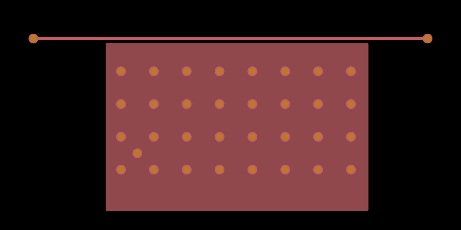
In the image above, notice the four-by-eight grid and the off-grid anchor via at the lower left. The pour stops short of the SIG route along the top, and no via sits between them.
JITX does not check the pitch against the substrate. With the sample
substrate’s via at a 0.5 mm pitch, we get drills 0.2 mm apart, under its
0.254 mm min_hole_to_hole, and no issue.
layout_stitched_pour
refuses, before it builds the rule, a pitch below the via pad’s size, which
would thin the grid, or one that puts the drills closer than
min_hole_to_hole. Stitch vias take the pour’s net, and clearance is not
enforced between copper of the same net, so neighboring via pads need no
copper spacing.
Fencing#
We fence a pour’s outline with a
fence_via rule keyed on
the pour’s tag, which lays rows of vias along the outline by a
ViaFencePattern, as
fenced_pour_outline does
around an antipad.
We fence a route through its routing structure, with
RoutingStructure.Layer.fence. A
fence_via rule fences no route, whether keyed on the route’s tag or its
net’s tag, and raises no issue.
A grounded coplanar line#
A coplanar RF feed with two rows of fence vias takes a routing structure whose layer carries a fence:
class RFLineTag(Tag):
    """RF nets that take the coplanar structure."""

def cpwg_structure() -> RoutingStructure:   # call it inside __init__
    pattern = checked_fence_pattern(
        ViaFencePattern(pitch=1.0, offset=0.6, initial_offset=0.45, num_rows=2),
        SampleSubstrate.THVia,
        coplanar_gap(0.2, 0.2),   # the structure's clearance, the gap rule's
    )
    layer = RoutingStructure.Layer(
        trace_width=0.3, clearance=0.2, velocity=150e9, insertion_loss=0.01
    ).fence(SampleSubstrate.THVia, pattern, reference_layer=0)
    return RoutingStructure({0: layer}, impedance=50, name="CPWG_50")
A routing_structure rule on RFLineTag applies it, as in Routing structures
by tag, to a code route between two RF pads. A GND
pour on layer 0 is the coplanar ground, starting 0.21 mm from the trace edge,
and the fence vias tie it to a GND plane on layer 1.
With no clearance rule between the line’s tag and the ground net’s tag, a board
clearance rule that matches the line and is wider than the structure’s 0.2 mm
clearance widens the gap to its own value plus 0.01 mm at any priority from 0
to 3, and nothing reports it. A keep-away from RFLineTag to AnyObject
widens it too, so write the keep-away against the noisy net’s tag, as the next
section does. Keep board clearance rules no wider than the narrowest gap a line
on the board needs, and set this line’s gap with a rule between its tag and the
ground net’s tag. At priority 2, the rule holds the gap against a wider board
clearance rule lower on the ladder, while a wider board clearance rule higher
on the ladder still widens it:
class GroundTag(Tag):
    """The ground net the coplanar gap is measured to."""

class CPWGLine(Circuit):
    def __init__(self) -> None:
        ...   # the RF and GND nets, the route, the pours, the structure rule
        GroundTag().assign(self.gnd)
        self.gap_rule = design_constraint(
            RFLineTag(), GroundTag(), priority=2
        ).clearance(0.2)
Set the structure’s clearance and the rule to the same value: the gap comes out 0.01 mm past the wider of the two, so lowering the rule alone does not narrow it.
The first row’s pads stay out of the gap when
initial_offset, the
row’s distance from the trace edge, is at least the 0.21 mm gap plus half the
via pad: here 0.45 mm against 0.21 + 0.225 = 0.435 mm. JITX does not check
this, and will place fence pads closer to the trace than the fab floor, so the
structure above passes its pattern through
checked_fence_pattern,
which refuses a pattern that fails it. The gap it checks against comes from
coplanar_gap, given the
structure’s clearance and the clearance of the rule that wins between the line
and its ground.
The coplanar pour runs past both of the line’s pads, so the fence vias that
wrap each end of the line land on ground. Each region of a coplanar pour needs
a ground via of its own, and fence vias do not count. Ended at the centers of
the line’s two pads, the pour is cut in two by the line and its pads; with the
anchor via in one half removed, that half is gone and the design still reports
No design issues. The design’s pour is one region, with an anchor via on
each side of the line.
In the image above, notice the narrow gap between the trace and the ground on
each side, with both fence rows inside the ground along the line, the outer
row wrapping its end, and an anchor via above and below the rows. The full design is
layout_cpwg_two_row_fence.
Keeping an RF line away from a switch node#
To keep an RF line away from one noisy net, we write the clearance between a tag on each net:
class RFTag(Tag):
    """Sensitive RF nets."""

class NoisyTag(Tag):
    """Noisy nets, such as a converter's switch node."""

class RFNearSwitchNode(Circuit):
    def __init__(self):
        ...   # self.rf and self.sw are the RF and switch-node nets; the RF
        # route crosses a switch-node pour and a GND pour
        RFTag().assign(self.rf)
        NoisyTag().assign(self.sw)
        self.rf_to_noisy = design_constraint(
            RFTag(), NoisyTag(), priority=5
        ).clearance(1.0)
The switch-node pour that the RF line crosses stands 1.01 mm from it on both
sides. The rule applies only between copper carrying RFTag and copper
carrying NoisyTag, so the GND pour keeps the spacing the other rules give it.
The design comes from
layout_sensitive_net_clearance.
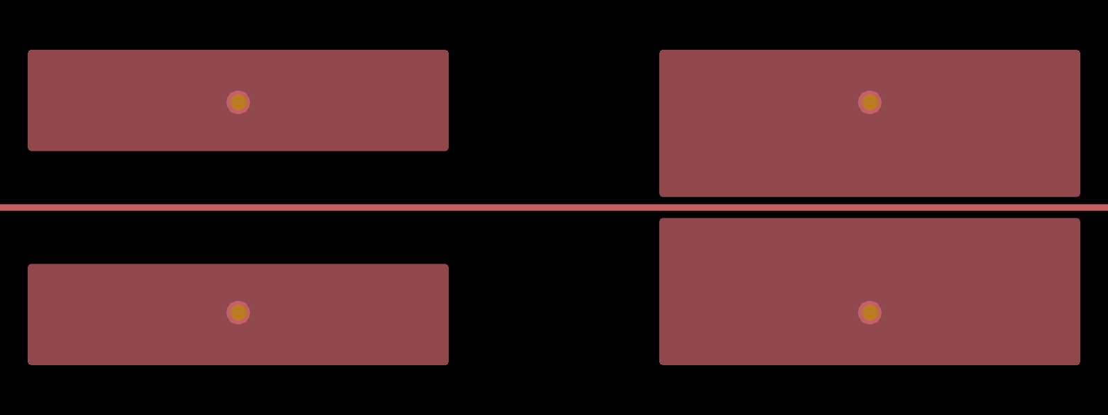
In the image above, notice the wide gap between the line and the switch-node pour on the left, against the narrow gap to the ground pour on the right.
Thermal relief#
A relief rule acts on every pad its condition matches, and the voids and spokes are part of the pour’s computed shape. A rule on a net’s tag relieves all of the net’s pads, and the vias placed on the net in code. To treat some of a net’s pads differently, we tag those pads, their landpattern or their component.
A condition is made of tags and nothing else, so no rule can select pads by
size. To give small and large pads different reliefs, the circuit in
layout_thermal_classes
calls that module’s
tag_pads_by_size,
which walks each part’s Pad objects with
visit and tags each pad
SmallPadRelief
or
LargePadRelief
by its size. Then one rule per class sets the relief:
from jitxexamples.patterns.layout_thermal_classes import (
    LargePadRelief, SmallPadRelief, tag_pads_by_size
)

class ThermalClasses(Circuit):
    def __init__(self):
        ...   # small, large, untagged and power parts on GND in one GND pour
        for part in (self.small, self.large, self.power):
            tag_pads_by_size(part)   # under 1.0 mm on the narrow side is small
        small = design_constraint(SmallPadRelief(), priority=3)
        large = design_constraint(LargePadRelief(), priority=3)
        self.small_relief = small.thermal_relief(0.2, 0.2, 2)
        self.large_relief = large.thermal_relief(0.3, 0.4, 4)
Each small pad gets a 0.2 mm gap and two narrow 0.2 mm spokes, and each large
pad a 0.3 mm gap and four 0.4 mm spokes for current. The untagged part, a
copy of the large part, is left out of the loop, and with no IsPad default
its pads join the pour solid. On a real board, keep the IsPad relief
default from Defaults above the fab floor
under these classes, so a pad the loop misses still gets a relief.
There is no separate direct-connect effect, so the power part’s 3.0 mm exposed
pad joins solid through
DirectConnectTag
and a relief whose spokes overlap until no gap is left, because each is as
wide as the pad’s diagonal. The diagonal comes from the pad’s width and
height, which
pad_size reads
from its copper shape:
from jitxexamples.patterns.layout_thermal_classes import (
    DirectConnectTag, pad_size
)

class ThermalClasses(Circuit):
    def __init__(self):
        ...   # as above, through the class rules
        exposed = self.power.landpattern.exposed
        DirectConnectTag().assign(exposed)
        width, height = pad_size(exposed)
        diagonal = (width**2 + height**2) ** 0.5
        direct = design_constraint(DirectConnectTag(), priority=4)
        self.direct_connect = direct.thermal_relief(0.2, diagonal, 4)
The pad also carries LargePadRelief from its size, and the direct connect
wins at priority 4.
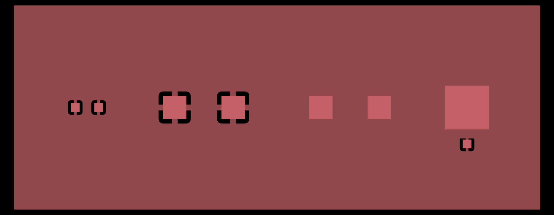
In the image above, from the left, the small part’s pads have two spokes each and the large part’s pads have four. The untagged copy of the large part, third from the left, meets the pour on every side. So does the power part’s exposed pad on the right, while the small sense pad below it has two spokes.
Heavy copper on one layer#
A 2 oz layer needs wider traces and gaps than
a 1 oz one. On a four-layer board whose layer 1 is 2 oz, we give that layer
floors: a width for every trace on it and a clearance for all of its copper,
keyed on OnLayer(1) at priority 1. A floor at 1 loses to every rule higher on
the ladder that matches the same copper, and nothing reports it, so each
PowerTag rule at 2 gets a copy narrowed to layer 1, at priority 3 and at the
floor. The board’s trace-to-pour rule sits at 1, below the net-tag rules, so a
tag’s own clearance to pours wins over it. On layer 1 it would beat the
clearance floor, so it gets a layer 1 form at the larger of its value and the
floor, 0.35 mm:
self.rules = [
    design_constraint(IsTrace).trace_width(0.2),
    design_constraint(IsCopper, IsCopper).clearance(0.15),
    design_constraint(IsTrace, IsPour, priority=1).clearance(0.2),
    design_constraint(PowerTag(), priority=2).trace_width(0.4),
    design_constraint(PowerTag(), AnyObject, priority=2).clearance(0.3),
    # layer 1's floors
    design_constraint(IsTrace & OnLayer(1), priority=1).trace_width(0.5),
    design_constraint(IsCopper & OnLayer(1), AnyObject, priority=1).clearance(0.35),
    design_constraint(IsTrace & OnLayer(1), IsPour, priority=1).clearance(0.35),
    # the PowerTag rules' copies on layer 1
    design_constraint(PowerTag() & OnLayer(1), priority=3).trace_width(0.5),
    design_constraint(PowerTag() & OnLayer(1), AnyObject, priority=3).clearance(0.35),
]
At mid-span, the power route is 0.4 mm wide on layers 0 and 2 with its ground
pour 0.31 mm away, and 0.5 mm wide on layer 1 with the pour 0.36 mm away. An
untagged route is 0.2 mm wide with the pour 0.21 mm away on layer 0, and
0.5 mm with 0.36 mm on layer 1. Built without the copies, the power route on
layer 1 kept its 0.4 mm width and 0.31 mm pullback, below both floors, and
nothing reported it. Written with
OnLayer.internal() in place of
OnLayer(1), the floors would also apply on layer 2, the other inner layer.
The full design is
layout_heavy_copper_layer.
Its
heavy_layer_index finds
the heavy layer from the substrate’s conductor thicknesses, and its
heavy_layer_rules writes
the floors, the trace-to-pour rule’s layer form and the copies from the rules
you pass it.
Keep each requested width at or below the pads the route ends on. Here the
routes end on 1.0 mm PowerVia pads, so the 0.5 mm floor fits. A request
wider than the 1.0 mm pads came back as the convex hull of the two pads, 1.0 mm
wide, and nothing reported it.
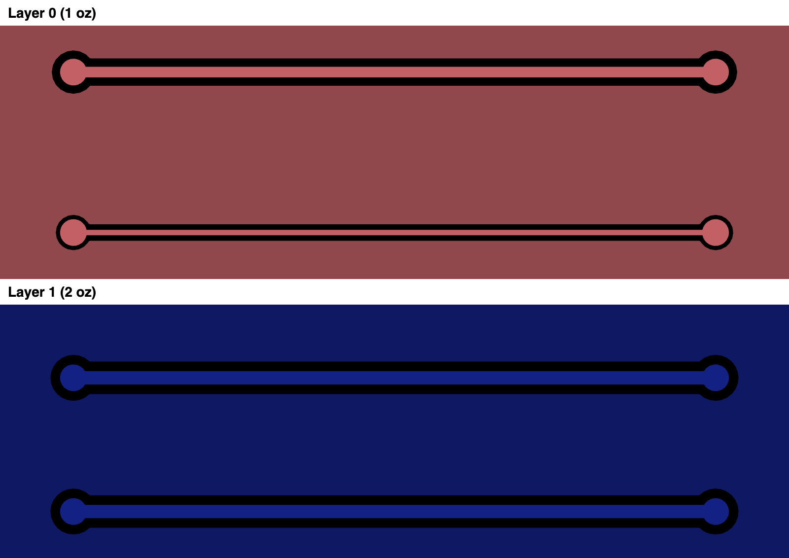
In the image above, the upper route in each strip is the power net and the lower one is untagged. On layer 0 the untagged route is narrower than the power route; on layer 1, at the bottom, both come out at the floor’s width and stand farther from the pour.
Board edge and cutouts#
Two implicit tags name the board’s openings:
IsBoardEdge matches the outer edge of the
outline only, and IsHole matches a hole in the
outline, a Cutout and a via’s
drill. Each takes a
rule:
class EdgeAndCutout(Circuit):
    def __init__(self):
        ...   # a GND pour, its anchor via, a cutout, and a via on another net;
        # the slot is a hole in the board outline's polygon
        edge = design_constraint(IsBoardEdge, AnyObject, priority=5)
        hole = design_constraint(IsHole, AnyObject, priority=5)
        self.edge_rule = edge.clearance(1.5)
        self.hole_rule = hole.clearance(0.5)
A ground pour then stops 1.51 mm from the outer edge and 0.5 mm from a slot, a
cutout and another net’s via drill. Without the rules, it stops 0.51 mm from the
edge, set by min_copper_edge_space, and 0.206 mm from the slot and cutout.
Because IsHole matches via drills, a hole rule also holds pours back from
the drill of every other-net via, even with the other side narrowed to
IsPour. Both rules are in
layout_edge_and_cutout.
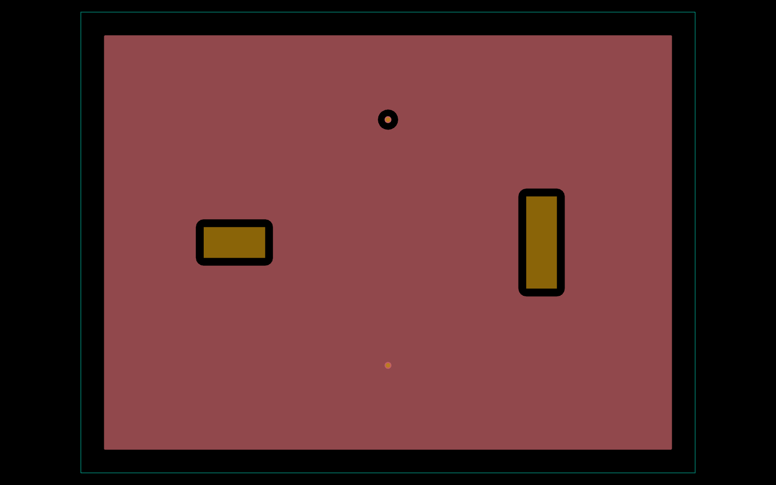
In the image above, notice the band between the pour and the outer edge, and the pullback around the cutout on the left and the slot on the right. The other net’s via near the top sits in a clear ring, and the pour’s own via below it is joined to the pour.
Checking that a rule applied#
The quick look is in the JITX board view. Select a route there and press B, and a Constraints panel shows which width rule the route took.
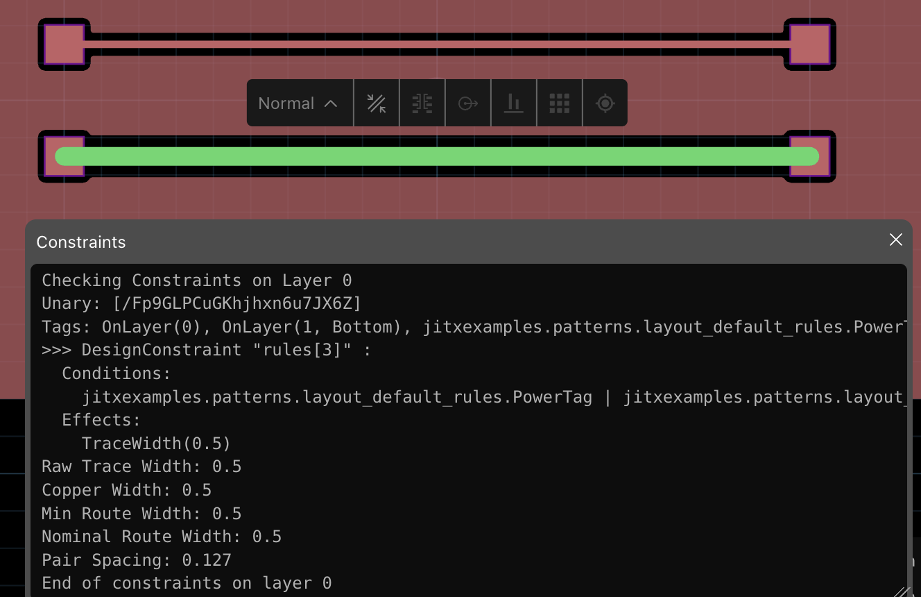
In the image above, taken on layout_default_rules, for the selected VCC
route, notice layer 0 and the route’s tags at the top, then the power width
rule listed as rules[3] from the design’s self.rules, with its
TraceWidth(0.5) effect, and the 0.5 mm widths it resolves to. The module’s
rule covers ground too, keyed on PowerTag() | GroundTag(), so the condition
in the panel goes on past PowerTag where our fragment has PowerTag() alone.
To check a value from a test, we capture the design and read its geometry.
After
capture,
root holds the design as the runtime
built it. Each Pour.shape is then the pour’s computed copper with its holes,
or Empty for a pour the runtime removed, and
a route’s traces hold its copper. With a
runtime started by jitx runtime start --background in the project root, we
submit
layout_default_rules_design,
the design of layout_default_rules:
import jitx
from shapely import union_all
from jitxexamples.patterns.layout_default_rules import layout_default_rules_design

with jitx.runtime as r:
    rd = r.submit(layout_default_rules_design)
    rd.capture(wait=20)
    c = rd.root.circuit

    pour = c.gnd_pour.shape.to_shapely().g   # computed copper, holes included
    shapes = [s for t in c.vcc_route.traces for s in t.shapes]
    print([s.geometry.width for s in shapes])                    # [0.5]
    print(pour.distance(union_all([s.to_shapely().g for s in shapes])))  # about 0.31
    print(rd.issues(satisfied=True).text())
The VCC trace here comes back as a polyline with a width. A trace that comes
back as a polygon, such as the hull in Heavy copper on one
layer, has no width, so measure it from its
geometry.
A query for Via
returns the vias our code placed together with the ones stitch and fence rules
generated, so you can count a stitch grid or measure a fence row.
The rules on this page surface in the
issues report in three ways: a
timing path with a missing routing structure, whether routing is satisfied, and
a route the rules leave no room for, reported as
Unrealizable Route: Insufficient space.
Fence pads closer to the trace than the fab floor, stitch drills closer than
min_hole_to_hole, stitch vias placed where a removed pour was, and a
fence_via rule that placed no vias raise no issue, so we confirm those by
measuring the copper.