Schematic Symbol Statements
The pcb-symbol statement defines an object that encodes the schematic representation of a part. This definition includes:
- The electrical connection points for the symbol (ie, the pins).
- The geometric artwork for the symbol.
- Text annotations such as part number, designator, etc.
Each pcb-symbol defines an internal coordinate frame. All of the geometry, pins, and other features of the symbol are defined with respect to that internal coordinate frame.
The JITX OCDB has a large collection of predefined symbols you can use directly or as templates. The make-box-symbol() function is a powerful tool to quickly create a consistent looking part library.
For more information about how pcb-symbol definitions are used, see the symbol statement as it applies to the pcb-component definition.
Signature
pcb-symbol symbol-name (arg1:Type1, ...) :
  name = <String|False>
  description = <String|False>
  preferred-orientation = <SymbolOrientation|False>
  backend-substitution(<String>) = <SchematicSymbol>
  <PIN-1>
  ...
  <LAYER-1>
  ...
The expression name symbol-name uniquely identifies this symbol definition
in the current context.
The argument list (arg1:Type1, ...) is optional and provides a means of
constructing parameterized symbol definitions.
- Parameters
name- This name is used in the UI as a more human readable name. If this string is not provided, then thesymbol-nameexpression is used as the symbol's name.description- This string provides documentation and further context when needed.- preferred-orientation - Marks the preferred rotational orientation of this symbol. Default is no preference for any particular orientation.
- backend-substitution - Tool for swapping a schematic symbol depending on which export backend is being used.
<PIN-1>- A pin statement which defines a connection point to the symbol in the symbol's coordinate frame.<LAYER-1>- A layer statement which provides a means of inserting symbol artwork into the symbol's coordinate frame.
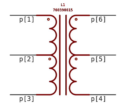
Non-Box Symbol Example
For more unusual components where box symbols may not apply, you can draw symbols the same way you can draw any collections of shapes in JITX. On imported components, the symbols may appear as collections of lines, shapes, and text.
; Wurth 760390015
pcb-symbol sym-760390015 :
  val L = 5.08
  val font-size = 1.0
  pin p[1] at Point(-5.080, 7.620) with :
    direction = Left
    length = L
    name-size = font-size
  pin p[2] at Point(-5.080, 0.0) with :
    direction = Left
    length = L
    name-size = font-size
  pin p[3] at Point(-5.080, -7.620) with :
    direction = Left
    length = L
    name-size = font-size
  pin p[4] at Point(5.080, -7.620) with :
    direction = Right
    length = L
    name-size = font-size
  pin p[5] at Point(5.080, 0.0) with :
    direction = Right
    length = L
    name-size = font-size
  pin p[6] at Point(5.080, 7.620) with :
    direction = Right
    length = L
    name-size = font-size

  layer("value") = Text(">VALUE", 0.7056, C, loc(0.0, 8.620))
  layer("reference") = Text(">REF", 0.7056, C, loc(0.0, 9.620))
  layer("foreground") = Circle(-2.794, 6.858, 0.254)
  layer("foreground") = Circle(2.540, 6.858, 0.254)
  layer("foreground") = Circle(2.540, -0.762, 0.254)
  layer("foreground") = Circle(-2.540, -0.762, 0.254)
  layer("foreground") = Polyline(0.254, [
    Point(-5.080, 7.620)
    Point(-2.540, 7.620)])
  layer("foreground") = Polyline(0.254, [
    Point(-0.6, -7.620)
    Point(-0.6, 7.620)])
  layer("foreground") = Polyline(0.254, [
    Point(0.6, -7.620)
    Point(0.6, 7.620)])
  layer("foreground") = Polyline(0.254, [
    Point(5.080, -7.620)
    Point(2.540, -7.620)])
  ; Coils
  layer("foreground") = Polyline(0.254, [
    Point(-5.080, 0.0) ; Center Tap
    Point(-2.540, 0.0)
    Arc(-2.540, 1.270, 1.270, 270.000, 180.0)
    Arc(-2.540, 3.810, 1.270, 270.000, 180.0)
    Arc(-2.540, 6.350, 1.270, 270.000, 180.0)
    Point(-2.540, 7.620)
    Point(-5.080, 7.620)
  ])
  layer("foreground") = Polyline(0.254, [
    Point(5.080, 7.620)
    Point(2.540, 7.620)
    Arc(2.540, 6.350, 1.270, 90.000, 180.000)
    Arc(2.540, 3.810, 1.270, 90.000, 180.000)
    Arc(2.540, 1.270, 1.270, 90.000, 180.000)
    Point(2.540, 0.0) ; Center Tap
    Point(5.080, 0.0)
  ])
  layer("foreground") = Polyline(0.254, [
    Arc(2.540, -1.270, 1.270, 90.000, 180.000)
    Arc(2.540, -3.810, 1.270, 90.000, 180.000)
    Arc(2.540, -6.350, 1.270, 90.000, 180.000)
    Point(2.540, -7.620)
    Point(5.080, -7.620)
  ])
  layer("foreground") = Polyline(0.254, [
    Point(-5.080, -7.620)
    Point(-2.540, -7.620)
    Arc(-2.540, -6.350, 1.270, 270.000, 180.000)
    Arc(-2.540, -3.810, 1.270, 270.000, 180.000)
    Arc(-2.540, -1.270, 1.270, 270.000, 180.000)
  ])
This generates a symbol that looks like this:
Statements
Here is the list of all of the statements you can use in a pcb-symbol :
| Statement | Description |
|---|---|
backend-substitution | Backend Substition |
description | Description |
layer | Layer |
name | Name |
pin | Pin |
preferred-orientation | Preferred Orientation |