pcb-stackup
The pcb-stackup statement is used to define the physical layer stack for the PCB. This includes the copper, dielectric, and soldermask layers. The definitions inside the pcb-stackup statement are used to inform the JITX runtime about the available copper layers and other features.
Signature
pcb-stackup stackup-name (arg1:Type1, ...) :
  name = <String|False>
  description = <String|False>

  <LAYER-1>
  ...
The expression name stackup-name uniquely identifies this stackup definition
in the current context.
The argument list (arg1:Type1, ...) is optional and provides a means of
constructing parameterized stackup definitions.
- Required Parameters
<LAYER-1>- The stackup is composed of multiple layer() statements which define the construction of the stackup. Each layer can be a different material.
- Optional Parameters
name- This name is used in the UI as a more user friendly name. If this string is not provided then thestackup-nameexpression is used as the stackup's name.description- This string is defining more meta-data for the stackup - such as the fabricator or manufacturer of this stackup.
Usage
A typical stackup will consist of multiple copper layers separated by resin core and prepreg layers. Here is an example of a 8-layer construction typical of controlled impedance applications:
pcb-material soldermask :
  type = Dielectric
  dielectric-coefficient = 3.2
  loss-tangent = 0.012

pcb-material copper:
  type = Conductor

pcb-material prepreg-2x2113:
  type = Dielectric
  dielectric-coefficient = 4.2
  loss-tangent = 0.02

pcb-stackup std-stackup :
  name = "8-layer 1.6mm"
  val cu-1oz = 0.035
  val H = 0.1524
  layer(0.019, soldermask)
  layer(cu-1oz, copper)
  layer(H, prepreg-2x2113)
  layer(cu-1oz, copper, "GND1")
  layer(H, prepreg-2x2113)
  layer(cu-1oz, copper, "SIG1")
  layer(H, prepreg-2x2113)
  layer(cu-1oz, copper, "GND2")
  layer(H, prepreg-2x2113)
  layer(cu-1oz, copper, "PWR1")
  layer(H, prepreg-2x2113)
  layer(cu-1oz, copper, "GND3")
  layer(H, prepreg-2x2113)
  layer(cu-1oz, copper, "SIG2")
  layer(H, prepreg-2x2113)
  layer(cu-1oz, copper)
  layer(0.019, soldermask)
In this example, all of the layers are separated by a 2x2113 ply prepreg dielectric. The copper layers are all 1oz/ft^2 (35um) thickness.
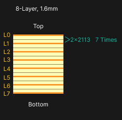
The strings on the inner copper layers provides overriding names for the copper layers. These names will be used in the layer visualizer to provide an easier mnemonic.
Complex Prepreg Ply Structure
In order to achieve the desired dielectric thickness required for some applications, we need to combine different ply constructions together. We can do this by defining separate materials for each prepreg.
Here is a 4-layer construction where the prepreg layer is a combination of a 1x2113 and 1x2116:
pcb-material core-FR4 :
  type = Dielectric
  dielectric-coefficient = 4.5
  loss-tangent = 0.008

pcb-material soldermask :
  type = Dielectric
  dielectric-coefficient = 3.2
  loss-tangent = 0.012

pcb-material copper:
  type = Conductor

pcb-material prepreg-FR4-2113:
  type = Dielectric
  dielectric-coefficient = 4.5
  loss-tangent = 0.008

pcb-material prepreg-FR4-2116:
  type = Dielectric
  dielectric-coefficient = 4.5
  loss-tangent = 0.008

pcb-stackup prepreg-stackup :
  name = "4-layer 1.6mm"
  layer(0.019, soldermask)
  layer(0.035, copper)
  layer(0.0762, prepreg-FR4-2113)
  layer(0.1067, prepreg-FR4-2116)
  layer(0.035, copper)
  layer(1.0, core-FR4)
  layer(0.035, copper)
  layer(0.1067, prepreg-FR4-2116)
  layer(0.0762, prepreg-FR4-2113)
  layer(0.035, copper)
  layer(0.019, soldermask)
Constructs the following stackup:
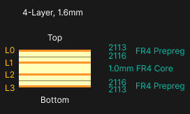
Notice that the 2113 and 2116 ply prepreg layers are adjacent to each other. This will allow us to construct an accurate PCB stackup table in the drawings.
Checks on Invalid Stackups
One limitation of the pcb-stackup is that Conductor type material layers must be separated by a Dielectric layer.
For example, if we construct a pcb-stackup with two adjacent copper layers:
pcb-stackup invalid-stackup :
  name = "2-layer 1.6mm"
  layer(0.019, soldermask)
  layer(0.035, copper)
  ; Invalid Copper Layer Here!
  layer(0.035, copper)
  layer(1.0, core-FR4)
  layer(0.035, copper)
  layer(0.019, soldermask)
This will throw the following exception when we use this stackup in the board for the current design:
Uncaught Exception: Stackups cannot have two adjacent conductor layers.
Using Generators
Generators are method of composition. In the pcb-stackup, we can use a generator to help reduce duplication in our stackup generation.
Note - This is a more complex example. Fear not! These structures will make sense as you gain more experience in the JITX environment.
This example builds on the pcb-material definitions from the 8-layer example stackup above:
defn add-layer (
  H:Double, cu:Double,
  --
  di-mat:Material = prepreg-FR4-2x2113,
  cu-mat:Material = copper
  cu-name:String = ?
  ):
  inside pcb-stackup:
    layer(H, di-mat)
    match(cu-name):
      (cu-n:One<String>):
        layer(cu, cu-mat, value(cu-n))
      (_:None):
        layer(cu, cu-mat)

pcb-stackup prepreg-stackup :
  name = "8-layer 1.6mm"
  val cu-1oz = 0.035
  val H = 0.1524
  layer(0.019, soldermask)
  layer(cu-1oz, copper)
  add-layer(H, cu-1oz, cu-name = "GND1")
  add-layer(H, cu-1oz, cu-name = "SIG1")
  add-layer(H, cu-1oz, cu-name = "GND2")
  add-layer(H, cu-1oz, cu-name = "PWR1")
  add-layer(H, cu-1oz, cu-name = "GND3")
  add-layer(H, cu-1oz, cu-name = "SIG2")
  add-layer(H, cu-1oz)
  layer(0.019, soldermask)
The inside pcb-stackup expression converts the function add-layer into a generator. When this function is called from a pcb-stackup context, it can generate statements into statements like layer() into the parent pcb-stackup context. If you were to call this function from a different context (eg, from a pcb-module), then this function would throw an error because the layer() statement would be unknown in that context.
In this case, the add-layer generator injects a dielectric layer and a copper layer with thicknesses based on the H and cu arguments, respectively. It uses default arguments for the dielectric and conductor materials to reduce the number of arguments we must pass.
The cu-name:String = ? is a special kind of default argument. You can think of cu-name not as a pure String but as a Maybe<String> - see stanza's reference on Maybe for more info. This drives the need for the match statement on the cu-name argument to differentiate between None and One<String>.
The constructed pcb-stackup object from this excerpt should match the 8-Layer stackup defined here.
Statements
| Statement | Description |
|---|---|
layer | Define a layer in the stackup |