JITX Official Documentation
Welcome to the official documentation of JITX. Here you'll find function references, tutorials, how-to guides, FAQs, and all of the information you need to learn and use JITX.
What Is JITX?
JITX is a tool that helps you design PCBs with automation of circuit design, component selection, component modeling, pin assignment, geometric constraints, schematic drafting, schematic verification, and more. You can design at the system level and automate the rest.
New Users / Getting Started / How To Start
If you're new to using JITX, welcome! A background in electrical engineering is all you need to get up and running designing boards in JITX.
For new users, we recommend reading through this page, then starting with the Tutorials, which will give you a quickstart to setting up and using JITX for your designs. Specifically, checkout the workflows below for a path to get started:
Suggested Onboarding Workflows
First Time User - End to End Design
- Setup and install JITX with JITX Installation Instructions.
- Design a basic board in JITX and export to CAD - do Quickstart 1
- Organize your schematic and layout with Quickstart II: Organize a schematic
- Export to CAD (KiCad or Altium) by following Exporting to CAD
- Layout the PCB in CAD the same way that you normally would.
Working with Existing Projects
- Import your design from CAD
- Revise your design in JITX
- Export your design back into CAD
Checking Designs
- Follow Write a check
- Follow Analyze a design
Creating Components
In Depth
- Follow First Time User, Checking Designs, and Creating Components Workflow.
- Follow Learn JITX
- Follow Quickstart III: Check a design
How To Use These Docs
Use the left side bar to move around the documentation (you can open the left side bar by clicking the ☰ in the top left of this page), and use the search bar above to search for functions, questions, tutorials, etc.
Install
Follow this tutorial to get JITX setup on your own system: Installing JITX
How Do I Get Help?
If you haven't been able to answer your questions by looking through the tutorials and using the search bar above, you can get help from JITX Inc. directly using one of the methods below.
VSCode Extension Method
This method assumes you have JITX installed in VSCode.
- Open VSCode.
- Click the "JITX" extension icon in the left side bar.
- Click the hamburger menu in the top left that looks like this: ☰
- Click "Request help"
- Fill out the form. We'll get back to you right away.
Web Method
If the VSCode extension method doesn't work for you, you can fill out this form to request help, we'll get back to you right away: https://support.jitx.com/hc/en-us/requests/new
Resources
- JITX Official Website
- JITX Github
- Learning Stanza (the programming language that JITX uses): http://lbstanza.org/stanzabyexample.html
- JITX Demo Videos
- https://www.youtube.com/watch?v=PkfMr6CSR60 - Software defined electronics.
- https://www.youtube.com/watch?v=ebKaLhxQn8Y - Create a new design.
Documentation Overview/Sections
The organization of the docuementation is as follows (see the side bar for a full index of the documentation).
- JITX Documentation Introduction - intro to the docs.
- Reference
- Reference materials are the low-level documentation of JITX. The Reference materials refer to technical descriptions of JITX's machinery and its operation. Things like descriptions of key classes, functions, and APIs
- Tutorials
- Tutorials are small, rewarding projects that help you learn JITX.
- How-To Guides
- How-to guides take you through a series of steps to help you solve a specific real world problem. They are tools for practitioners who are trying to get something done using JITX.
- Open Component Database (OCDB)
- The Open Components Database (OCDB) is an open database of components and circuit generators for automated circuit board design. This section provides users with quick access to information on how to use everything in OCDB with examples.
- BOM Import Data Format
- Describes how to import a BOM.
- Example Designs
- The example designs consists of projects exemplifying common use cases.
- Frequently Asked Questions
- This section contains questions that users frequently encounter.
Documentation Index
You can access the index of the entire docs in the left hand side panel.
JITX Reference
Reference materials refer to technical descriptions of JITX’s machinery and its operation. Things like descriptions of key classes, functions, and APIs would fall under this umbrella. This includes types, statements, and commands among other things.
- Types are classifications of circuit board concepts and define their possible values and operations.
- Statements are pieces of code, often one line each, that together define a design. Statements are what constructs ESIR (Electronic Systems Intermediate Representation) to create designs.
- Commands are function calls that retrieve information from or modify a design.
Examples
- Commands
pins (obj:JITXObject)retrieves all pins in the given JITXObject.set-rules (rules:Rules)assigns aRulesto your design.
- Statements
mpn = "TRS3122ERGER"assigns a component's mpn.port p : pin[2]creates a port with two pins.
- Types
- Top-level definitions have types including
LandPattern,SchematicSymbol, andBoard. They all subtypeJITXDef, meaning that objects with these types can perform the same operations as aJITXDef. - Local definitions have types including
LandPatternPadandSymbolPin. They all subtypeJITXObject.
- Top-level definitions have types including
JITX Statements
| Statement | Description |
|---|---|
pcb-board | Metadata of the board itself |
pcb-bundle | A collection of other top level statements |
pcb-check | A check on the correctness of our design |
pcb-component | A single device such as an IC or passive element. |
pcb-enum | A store for categorical variables |
pcb-landpattern | A component footprint/land pad. |
pcb-material | A material for a layer in the stackup |
pcb-module | A single reusable module which may contain other top level statements. |
pcb-pad | A single pad on the physical device/footprint |
pcb-rules | Fab house rules (tolerances, trace widths, |
pcb-routing-structure | Single-Ended Routing Structures |
pcb-differential-routing-structure | Differential Routing Structures |
pcb-stackup | The stackup for the board |
pcb-via | The via definition and parameters |
pcb-struct | A way to group several related variables. |
pcb-symbol | A schematic symbol |
Boards
A pcb-board statement defines the physical structure of the circuit board for a design. A board contains a stackup, boundary, signal boundary, and optional layer statements.
Signature
pcb-board board-name (arg1:Type1, ...):
  name = <String|False>
  description = <String|False>

  boundary = <Shape>
  signal-boundary = <Shape|False>
  stackup = <Stackup>

  vias = [<Via>, <Via>, ... ]

  layer(<LayerSpecifier>) = <Shape>
  ...
The expression name board-name uniquely identifies this board definition in the current context.
The argument list (arg1:Type1, ...) is optional and provides a means of constructing parameterized board definitions.
- Required Parameters
boundary- This is aShapethat defines the physical board outline.- This shape must be a simple polygon.
- This means that it must not have any holes or self-intersections.
stackup- User must provide a pcb-stackup definition.- This defines the copper and dielectric layer stackup.
vias- Tuple of pcb-via definitions.- These definitions limit what vias are allowed to be placed on the board.
- Only the vias present in this tuple will populate the drop-down via menu in the board tool.
- Optional Parameters
name- Optional string to provide a human readable name, mostly for the UI. If not present, then the expression name will be used.description- Optional string to describe this object. This is primarily for documentation and use in the UI.signal-boundary- This is an optionalShapethat defines what region of the board the router is allowed to route copper.- This shape must be a simple polygon.
- If not provided, the board definition will re-use the
boundaryshape for this parameter. - If provided, this shape must be no larger than the
boundaryshape. If this shape exceeds theboundaryshape, then the JITX runtime will raise an error.
layer()- Optional layer statements that allow the user to introduce geometry on any of the layers of the board.
Usage
The pcb-board definition is passed to the JITX runtime via the set-board function.
val board-shape = Rectangle(60.0, 40.0)
val my-stackup = ocdb/manufacturers/stackups/jlcpcb-jlc2313

pcb-via default-th:
  start = Top
  stop = Bottom
  diameter = 0.65
  hole-diameter = 0.4
  type = MechanicalDrill
  tented = true

pcb-board my-circuit-board :
  stackup = my-stackup
  boundary = board-shape
  signal-boundary = offset(board-shape, -0.5)
  vias = [default-th]

...

set-board(my-circuit-board)
The OCDB library has many predefined stackups that can be useful for building prototypes.
Notice the use of the offset function to construct a signal-boundary that is slightly inset from the board boundary.
Using Arguments
Parameterized board definitions can be useful when constructing common structures. Building on the previous example:
val STD-FIXTURE-SHAPE = RoundedRectangle(100.0, 40.0, 1.0)

pcb-board fixture-board (
  base-stackup:Stackup,
  --
  outline:Shape = STD-FIXTURE-SHAPE,
  sig-buffer:Double = 0.5
  ) :
  name = to-string("fixture-%_-%_" % [outline, sig-buffer])
  stackup = base-stackup
  boundary = outline
  signal-boundary = offset(outline, (- sig-buffer))
  vias = [default-th]

...

val my-stackup = ocdb/manufacturers/stackups/jlcpcb-jlc2313

; Example #1
val brd = fixture-board(my-stackup)
; Example #2
val brd = fixture-board(my-stackup, sig-buffer = 1.0)

set-board( brd )
In this example, we demonstrate the use of optional keyword arguments for parametrically defining the board for our design.
Here the sig-buffer argument is a keyword argument with a default value of 0.5. This forces the signal-boundary to be 0.5mm smaller than the boundary shape on all sides
of the board.
Making it a keyword argument provides better readability of the code - we don't have to wonder whether that second argument was supposed to be the outline shape or the sig-buffer.
It is often convenient to include a name constructed from the parameters so that we can differentiate two different pcb-board definitions constructed with this function.
Using Generators
Generators are a tool to compose reusable features into a definition.
defn set-boundary (outline:Shape -- sig-buffer:Double = 0.5) :
  inside pcb-board:
    boundary = outline
    signal-boundary = offset(outline, (- sig-buffer))

val board-shape = Rectangle(60.0, 40.0)

pcb-board circuit-board-2 :
  stackup = my-stackup
  vias = [default-th]
  set-boundary(board-shape)

...

set-board(circuit-board-2)
The set-boundary function is a generator. Notice the use of the inside pcb-board syntax. When set-boundary is called from within the context of a pcb-board definition, it can create any of the expected pcb-board parameters. In this particular instance, the set-boundary function sets the boundary and signal-boundary parameters.
The resulting circuit-board-2 definition would be equivalent to:
val board-shape = Rectangle(60.0, 40.0)

pcb-board equivalent-circuit-board :
  stackup = my-stackup
  vias = [default-th]
  boundary = board-shape
  signal-boundary = offset(board-shape, -0.5)
Calling set-boundary from any other context (ie, a regular function or a pcb-module) will elicit an error because the boundary = syntax will be unknown.
Name
name is the optional name field of a JITX object. Use it to store a descriptive name as a String. This name will often be used in the UI in place of the object's expression name for better readability.
Signature
name = <String>
Usage
Literal String Names
pcb-component component :
  name = "ADM7150"

pcb-module band-pass-filter :
  name = "Band-pass filter"
The examples name = "ADM7150" and name = "Band-pass filter" use a String liternal for the name.
Formatted Strings
pcb-pad smd-pad (anchor:Anchor, w:Double, h:Double) :
  name = to-string("%_x%_ %_ SMD Pad" % [w,h,anchor])

pcb-landpattern test-lp:
  pad p[1] : smd-pad(C, 0.6, 0.7) at loc(x0,y0)
We can also construct strings using formatting routes and parameter arguments for a particular definition. In this example, the constructed smd-pad name property would be 0.6x0.7 C SMD Pad
Description
description is the optional descriptive field of a JITX object. Use it to store a description of the object for human designers reading JITX, and to make the object easier to find via text search. This description also shows up in the UI, such as the design explorer, to provide more insight into particular components and modules in the design.
Signature
description = <String>
Examples
; We can use string literals to describe a particular component.
pcb-component analog-devices-ADM7150 :
  description = "800 mA Ultralow Noise, High PSRR, RF Linear Regulator"

; We can use string formatting to construct descriptions based on variables
;   or arguments to a JITX Definition
pcb-module band-pass-filter (high-cut:Double, low-cut:Double) :
  description = to-string("Band-pass Filter - Highpass = %_ Hz and Lowpass = %_ Hz.")
Layer
The layer statement is used to create geometry on the non-copper layers of a circuit board. The layer() statement is valid in the following contexts:
Signature
layer(<LayerSpecifier>) = <Shape>
<LayerSpecifier>- A LayerSpecifier instance that identifies which non-copper layer to apply the provided geometry to.<Shape>- AShapeinstance that defines the geometry that will be created on the specified layer.
Usage
The most common usage of the layer() statement is in pcb-landpattern:
pcb-landpattern diode-lp :
  pad c : smd-pad(0.4, 0.75) at loc(-1.25, 0.0) on Top
  pad a : smd-pad(0.4, 0.75) at loc(1.25, 0.0) on Top

  layer(Silkscreen("body", Top)) = LineRectangle(1.8, 1.0)
  layer(Silkscreen("body", Top)) = Line(0.1, [Point(-0.70, -0.5), Point(-0.70, 0.5)])
  layer(Courtyard(Top)) = Rectangle(3.2, 2.0)

  layer(ForbidCopper(LayerIndex(0))) = Rectangle(2.0, 1.0)
This will construct a landpattern that looks like this:
Notice the silkscreen in yellow with cathode marker. The blue box is the ForbidCopper layer on the Top Layer. Red is the top copper pads for the cathode c and anode a.
The white bounding rectangle is the Courtyard layer.
See LayerSpecifier for more information about specific layers.
Cutouts
When constructing cutouts in the board layout, your best bet is to use a solid region as opposed to a line. A line can confuse the routing engine into thinking that there are two physically separate regions where copper can be placed.
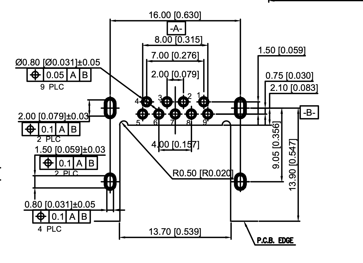
Consider a USB connector part, U231-096N-3BLRT06-SS, Jing Extension of the Electronic Co.
Here is an excerpt from the datasheet:
If we draw the cutout with a line, as shown in the datasheet, we get this:
pcb-landpattern USB-conn:
  ...

  layer(Cutout()) = Line(0.254, [Point(-7.300, -7.650), Point(-8.450, -7.650)])
  layer(Cutout()) = Polyline(0.254, [
    Point(6.850, 4.650)
    Point(6.850, -7.650)
    Point(8.450, -7.650)])
  layer(Cutout()) = Polyline(0.254, [
    Point(-6.850, 4.650)
    Point(-6.850, -7.650)
    Point(-7.300, -7.650)])
  layer(Cutout()) = Line(0.254, [Point(-6.850, 4.650), Point(6.850, 4.650)])
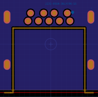
The cutout line is in gold color. Notice that the ground layer (blue) copper is present on both sides of the cut line with some margin in between. The routing engine basically thinks that the cutout is just the line. If we were making a slot - that would probably be reasonable. But for this case, we want the hole region between the cutout line and the board edge (red) to be a cutout region.
The right way is to use a Rectangle or Polygon solid geometry:
pcb-landpattern USB-conn :
  ...

  layer(Cutout()) = Polygon([
    Point(-6.850, 4.650), Point(6.850, 4.650),
    Point(6.850, -7.650), Point(-6.850, -7.65),
  ])
  layer(Cutout()) = Circle(Point(-6.85 + 0.5, 4.65), 0.5)
  layer(Cutout()) = Circle(Point(6.85 - 0.5, 4.65), 0.5)
Notice that the cutout region fills the entire connector region and the blue ground plane is not present in the cutout region.
Bundle Statements
A pcb-bundle definition groups a set of pins. Bundles can include ports and other bundles. You can connect bundles using a net statement, or use supports and require statements with bundles for automated pin assignment.
For example we can create a bundle for an i2c bus with the following statement:
pcb-bundle i2c:
  pin sda
  pin scl
Bundles can be parametric and include other bundles. Here is a definition for a bank of lvds pins of variable size:
pcb-bundle diff-pair :
  pin N
  pin P

pcb-bundle lvds-bank (width:Int) :
  port clk : diff-pair
  port data : diff-pair[width]
You can make bundles parametric to represent optional pins. Here's an example of a parametric SWD bundle, that can optionally include the SWO pin:
pcb-bundle swd (swo:True|False) :
  pin swdio
  pin swclk
  pin reset
  if swo :
    pin swo
Statements
Here is the list of all of the statements you can use in a pcb-bundle :
| Statement | Description |
|---|---|
name | Name of the bundle |
description | Description for the bundle |
ports | Creates elements you can connect to |
Name
name is the optional name field of a JITX object. Use it to store a descriptive name as a String. This name will often be used in the UI in place of the object's expression name for better readability.
Signature
name = <String>
Usage
Literal String Names
pcb-component component :
  name = "ADM7150"

pcb-module band-pass-filter :
  name = "Band-pass filter"
The examples name = "ADM7150" and name = "Band-pass filter" use a String liternal for the name.
Formatted Strings
pcb-pad smd-pad (anchor:Anchor, w:Double, h:Double) :
  name = to-string("%_x%_ %_ SMD Pad" % [w,h,anchor])

pcb-landpattern test-lp:
  pad p[1] : smd-pad(C, 0.6, 0.7) at loc(x0,y0)
We can also construct strings using formatting routes and parameter arguments for a particular definition. In this example, the constructed smd-pad name property would be 0.6x0.7 C SMD Pad
Description
description is the optional descriptive field of a JITX object. Use it to store a description of the object for human designers reading JITX, and to make the object easier to find via text search. This description also shows up in the UI, such as the design explorer, to provide more insight into particular components and modules in the design.
Signature
description = <String>
Examples
; We can use string literals to describe a particular component.
pcb-component analog-devices-ADM7150 :
  description = "800 mA Ultralow Noise, High PSRR, RF Linear Regulator"

; We can use string formatting to construct descriptions based on variables
;   or arguments to a JITX Definition
pcb-module band-pass-filter (high-cut:Double, low-cut:Double) :
  description = to-string("Band-pass Filter - Highpass = %_ Hz and Lowpass = %_ Hz.")
Ports
port is a JITX statement that defines the electrical connection points for a component or module.
The port statement can be used in the following contexts:
Each port statement in any of these contexts is public by default. This means that each port can be accessed externally by using dot notation.
Signature
  ; Single Port Instance
  port <NAME> : <TYPE>
  ; Array Port Instance
  port <NAME> : <TYPE>[<ARRAY:Int|Tuple>]
<NAME>- Symbol name for the port in this context. This name must be unique in the current context.<TYPE>- The type of port to construct. This can be the keywordpinfor a single pin type or any declaredpcb-bundletype.<ARRAY:Int|Tuple>- Optional array initializer argument. This value can be:Int-PortArrayconstructed with lengthARRAY. This array is constructed as a contiguous zero-index array.Tuple-PortArrayconstructed with an explicit set of indexes. This array is not guaranteed to be contiguous.
Watch Out! - There is no space between
<TYPE>and the[opening bracket of the array initializer.
Shortcut Alias
  ; Single Port - Pin Type
  pin <NAME>
The pin name statement is a shortcut for port name : pin
Syntax
There are multiple forms of the port statement to allow for flexible construction of the interface to a particular component. The following sections outline these structures.
Basic Port Declaration
The user has two options when declaring a single pin:
; Single Pin 'a'
port a : pin
; Equivalent to
pin a
The pin a structure is a shorthand version for declaring single pins.
Pin Arrays
To construct a bus of single pins, we use the array constructor:
port contiguous-bus : pin[6]
port non-contiguous-bus : pin[ [2, 5, 6] ]

println(indices(non-contiguous-bus))
; Prints:
; [2 5 6]
The contiguous-bus port is defined as a contiguous array of pins with indices: 0, 1, 2, 3, 4, & 5.
The non-contiguous-bus port is defined an array with explicit indices: 2, 5, & 6. The indices function is a helper function for determining what array indices are available on this port.
Attempting to access a port index that does not exist or is negative will result in an error.
There is no shorthand version for creating PortArray instances with the pin statement.
Bundle Port
A bundle port is a connection point that consolidates multiple individual signals into one entity. The structure of this port is defined by the pcb-bundle type used in its declaration:
pcb-bundle i2c:
  pin sda
  pin scl

pcb-module mcu:
  port data : i2c
In this example, we define the i2c bundle. Notice that this bundle is constructed from same port/pin statements defined above.
The data port is then constructed with the bundle name i2c as the type.
The individual signals of the data port are accessible using dot notation:
pcb-module top-level :

  inst U1 : mcu

  println(port-type(mcu.data.sda))

; Prints:
;  [SinglePin object]
Bundle Array Port
As with the single pin, we can construct port arrays of bundle types:
pcb-bundle i2c:
  pin sda
  pin scl

pcb-module mcu:
  port busses : i2c[3]
In this example, we construct a contiguous array of 3 I2C bus ports. We can access the individual signals of these busses as well:
pcb-module top-level :

  inst U1 : mcu

  println(port-type(mcu.busses[0].scl))

; Prints:
;  [SinglePin object]
Port Types
Each port has a type associated with it. That type can be accessed with the function port-type. This function returns a PortType instance that can be one of the following types:
SinglePin- A port instance of typepinBundle- A port instance of type BundlePortArray- An array of port instances
We would typically use the result of this function with a match statement:
pcb-module amp:

  port vout : pin[4]

  match(port-type(vout)):
    (s:SinglePin): println("Single")
    (b:Bundle): println("Bundle")
    (a:PortArray): println("Array")
This structure allows a different response depending on the type of port.
The Bundle PortType
The Bundle port type provides the user with access to the type of bundle that was used to construct this port:
pcb-bundle i2c:
  pin sda
  pin scl

pcb-module mcu:
  port bus : i2c

pcb-module top-level:
  inst U1 : mcu

  match(port-type(U1.bus)):
    (b:Bundle):
      println("Bundle Type: %_" % [name(b)])
    (x): println("Other")

; Prints:
; Bundle Type: i2c
Notice that the b object is a reference to the pcb-bundle i2c definition. This provides a convenient way to check if a given port matches a particular bundle type.
Walking a PortArray
It is often useful to walk a PortArray instance and perform some operation on each of the SinglePin instances of that PortArray. Because PortArray instances can be constructed from either single pins or bundles, they can form arbitrarily complex trees of signals. To work with trees of this nature, recursion is the tool of choice.
Note: This is a more advanced example with recursion. Fear not brave electro-adventurer - These examples will serve you well as you become more comfortable with the JITX Environment.
defn walk-port (f:(JITXObject -> False), obj:JITXObject) -> False :
  match(port-type(obj)):
    (s:SinglePin): f(obj)
    (b:Bundle|PortArray):
      for p in pins(obj) do:
        walk-port(f, p)

pcb-module top-level:
  port bus : i2c[3]

  var cnt = 0
  for single in bus walk-port :
    cnt = cnt + 1

  println("Total Pins: %_" % [cnt])

; Prints
; Count: 1
; Count: 2
; Count: 3
; Count: 4
; Count: 5
; Count: 6
The i2c bundle has 2 pins and there are 3 i2c ports in the array which results in 6 total pins.
In this example, we construct a Sequence Operator that will allow us to walk the pins of a port. The structure of a Sequence Operator is:
defn seq-op (func, seq-obj) :
  ...
Where the seq-obj is a Sequence of objects. The for statement will iterate over the objects in the seq-obj sequence and then call func on each of the objects in the sequence. The value returned by this function can optionally be captured and returned.
In our example, walk-port is a Sequence Operator that doesn't return any result. Notice how walk-port has replaced the do operator that we normally see in a for loop statement.
So where does the func function come from then? The for statement constructs a function from the body of the for statement. In this example, the function effectively becomes:
defn func (x:JITXObject) -> False :
  cnt = cnt + 1
Notice that this function is a closure. It is leveraging the top-level context to access the cnt variable defined before the for statement.
A similar construction in Python might look like:
  cnt = 0
  def func(signal):
    global cnt
    cnt = cnt + 1

  for x in walk-port(bus):
    func(x)
Where walk-port would need to be implemented as a generator
in python that constructs a sequence.
Check Statements
Checks are how we check our designs for correctness. We can write arbitrary code to scan through our designs, inspect the data and make sure the circuit will work as designed. The checking functions contain code that generates a well formatted report, that prompts us to enter more data or points out errors in our design.
ocdb/utils/checks has a large set of common checks, and code to apply those automatically checks to a design.
We can also define checks that are specific to a circuit or component. The goal is to create circuit generators that check themselves for correctness, making our design work more reusable.
Example check for AEC ratings
pcb-check aec-q200 (component:JITXObject):

    #CHECK(
    name =                 "Automotive rating"
    description =          "Check that a passive component is AEC Q200 rated"
    condition =            has-property?(component.aec-rating),
    category =             "Component Data"
    subcheck-description = "Check that %_ has a defined aec-rating" % [ref(component)],
    pass-message =         "%_ has a property for aec-rating of %_" % [ref(component) property(component.aec-rating)],
    info-message =         "%_ does not have an aec-rating property attached" % [ref(component)],
    locators =             [instance-definition(component)]
    )

    #CHECK(
    name =                 "Automotive rating"
    description =          "Check that a passive component is AEC Q200 rated"
    condition =            property(component.aec-rating) == "Q200",
    category =             "Component Checks"
    subcheck-description = "Check that %_ is AEC Q200 rated." % [ref(component)],
    pass-message =         "%_ is AEC Q200 rated" % [ref(component)],
    fail-message =         "%_ is not AEC Q200 rated. Instead has rating %_." % [ref(component) property(component.aec-rating)],
    locators =             [instance-definition(component)]
    )

    pcb-module checked-design :
      inst r : chip-resistor(1.0)
      check aec-q200(r)
Statements
Here is the list of all of the statements you can use in a pcb-check :
| Statement | Description |
|---|---|
#CHECK | Registers a check to add to report. |
#CHECK
We use #CHECK statements to evaluate conditions in our designs, and then show a Pass Add Info or Fail state.
Syntax
pcb-check aec-q200 (component:JITXObject):

    #CHECK(
    name =                 "Automotive rating"
    description =          "Check that a passive component is AEC Q200 rated"
    condition =            has-property?(component.aec-rating),
    category =             "Component Data"
    subcheck-description = "Check that %_ has a defined aec-rating" % [ref(component)],
    pass-message =         "%_ has a property for aec-rating of %_" % [ref(component) property(component.aec-rating)],
    info-message =         "%_ does not have an aec-rating property attached" % [ref(component)],
    locators =             [instance-definition(component)]
    )

    #CHECK(
    name =                 "Automotive rating"
    description =          "Check that a passive component is AEC Q200 rated"
    condition =            property(component.aec-rating) == "Q200",
    category =             "Component Checks"
    subcheck-description = "Check that %_ is AEC Q200 rated." % [ref(component)],
    pass-message =         "%_ is AEC Q200 rated" % [ref(component)],
    fail-message =         "%_ is not AEC Q200 rated. Instead has rating %_." % [ref(component) property(component.aec-rating)],
    locators =             [instance-definition(component)]
    )
Description
The above #CHECK statements generate this report, when run on a component with instance nae r[0].
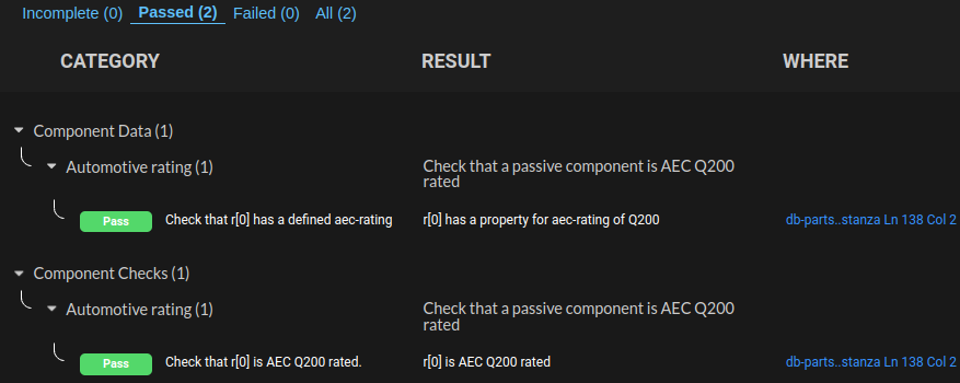
name The name of the check
description The top-level description of the check in the report
condition A boolean expression that evaluates to true or false. This condition defines if the check passes, or fails.
category The top-level category to organize this check in the report.
subcheck-description A detailed description of the result of this specific #CHECK
pass-message What should be printed in the report if condition resolves to true
fail-message What should be printed in the report if condition resolves to false and the #CHECK describes a design error. A #CHECK can have a fail-message or a pass-message but not both.
info-message What should be printed in the report if condition resolves to false and the #CHECK describes missing data. A #CHECK can have a fail-message or a pass-message but not both.
locators A list of code locators that help the reader of the report what specific aspect of the design needs attention when the #CHECK fails.
Components
A pcb-component definition models a single part that can be placed on a board. Components have ports, schematic symbols, a landpattern, and associated metadata.
Here is an example definition for an Epson FC-135 crystal oscillator:
pcb-component epson-fc-135 :
  name = "32.768kHz Crystal"
  description = "CRYSTAL 32.7680KHZ 7PF SMD"
  manufacturer = "Epson"
  mpn = "FC-135 32.768KA-AG0"

  port p : pin[[1 2]]

  val sym = crystal-sym(0)
  symbol = sym(p[1] => sym.p[1], p[2] => sym.p[2])
  landpattern = xtal-2-3215(p[1] => xtal-2-3215.p[1], p[2] => xtal-2-3215.p[2])
  reference-prefix = "Y"

  property(self.load-capacitance) = 7.0e-12
  property(self.shunt-capacitance) = 1.0e-12
  property(self.motional-capacitance) = 3.4e-15
  property(self.ESR) = 70.0e3
  property(self.frequency) = 32.768e3
  property(self.frequency-tolerance) = 20.0e-6
  property(self.max-drive-level) = 0.5e-6
Statements
Here is the list of all of the statements you can use in a pcb-component :
| Statement | Description |
|---|---|
description | Description for the component |
emodel | EModel for the component |
landpattern | Physical land-pattern/footprint for the component. Also mapped to component ports. |
manufacturer | Manufacturer of the component |
mpn | Manufacturer part number of the component |
name | Name of the component |
pin-properties | An easy way to map component ports to pins on a landpattern. |
ports | Ports usable when this component is instantiated in a module |
properties | Properties of the component or its ports. |
reference-prefix | Start of the reference designator (default is "U"). |
supports | Supported peripherals for automated pin solving. |
symbol | Schematic symbol for the component. Mapped to the defined ports. |
Description
description is the optional descriptive field of a JITX object. Use it to store a description of the object for human designers reading JITX, and to make the object easier to find via text search. This description also shows up in the UI, such as the design explorer, to provide more insight into particular components and modules in the design.
Signature
description = <String>
Examples
; We can use string literals to describe a particular component.
pcb-component analog-devices-ADM7150 :
  description = "800 mA Ultralow Noise, High PSRR, RF Linear Regulator"

; We can use string formatting to construct descriptions based on variables
;   or arguments to a JITX Definition
pcb-module band-pass-filter (high-cut:Double, low-cut:Double) :
  description = to-string("Band-pass Filter - Highpass = %_ Hz and Lowpass = %_ Hz.")
EModel
The emodel statement inside a pcb-component associates the component with an electrical model.
Syntax
; define a pcb-component with a resistor EModel
pcb-component my-resisor:
  emodel = Resistor(resistance-ohms, tolerance-%, max-power-watts)
Description
An emodel is a simplified model of electrical properties. More complete simulation models can be defined with spice statements (coming soon).
Introspection Command
The emodel? query command returns the electrical model of an instance or a component. The function returns false if there is no electrical model or the argument is not a single component instance.
Different types of EModel's:
; define a resistor EModel
  emodel = Resistor(resistance-ohms, tolerance-%, max-power-watts)

; define a capacitor EModel
  emodel = Capacitor(capacitance-farads,
                     tolerance-%,
                     max-voltage-volts,
                     polarized?, ; optional boolean
                     low-esr?,   ; optional boolean
                     temperature-coefficient?, ; optional string, eg "X7R" or "X5R"
                     dielectric? ; optional)   ; optional string, eg "Ceramic, "Tantalum", "Electrolytic"

; define an inductor EModel
  emodel = Inductor(inductance-microhenries, tolerance-%, max-current-amps)

; define a diode EModel
  emodel Diode(forward-current-amps,
               forward-voltage-volts,
               max-current-amps,
               max-reverse-voltage-volts,
               color?, ; optional, for LEDs
               luminous-intensity-millicandelas) ; optional, for LEDs
Example Code:
pcb-component cap-component :
  emodel = Capacitor(1.0e-007)
pcb-module my-design :
  inst cap : cap-component
  inst cap-array : cap-component[3]

  println("emodel of cap is %_" % [emodel?(cap)])
  println("emodel of cap-array[0] is %_" % [emodel?(cap-array[0])])
  println("emodel of cap-component is %_" % [emodel?(cap-component)])
The emodel? query returns Capacitor(1.0e-007) for all three calls.
The output is
emodel of cap is Capacitor(1.0e-007)
emodel of cap-array[0] is Capacitor(1.0e-007)
emodel of cap-component is Capacitor(1.0e-007)
Land Pattern
landpattern is an ESIR statement that associates a physical footprint/land-pattern with a component, and maps the ports of the component to the pads of the land-pattern.
Syntax
pcb-component inverted-f-antenna-cmp :
  description = "2.4 GHz Inverted F trace antenna"
  pin launch
  pin gnd
  val lp = ant-2GHz4-inverted-f-geom
  landpattern = lp(launch => lp.p[1], gnd => lp.p[2], gnd => lp.p[3], gnd => lp.p[4])

pcb-component amphenol-minitek127 (n-pins:Int) :
  description = "SMD Female 1.27mm pitch header"
  port p : pin[1 through n-pins]
  val lp = amphenol-minitek127-pkg(n-pins)
  landpattern = lp(for i in 1 through n-pins do: p[i] => lp.p[i])
Description
The land pattern statement specifies a land pattern to use, as well as a pad mapping. The general pattern is:
pcb-component my-component:
  pin component-pin-a
  pin component-pin-b
  landpattern = my-landpattern(component-pin-a => landpattern-pad-a, component-pin-b => landpattern-pad-b)
Where my-landpattern is the name of the pcb-landpattern, which has pads landpattern-pad-a and landpattern-pad-b.
The following snippet matches component port launch to the p[1] pad of the antenna-landpattern, and the component port gnd to three pads on the land pattern p[2], p[3], and p[4]. When we net to inverted-f-antenna-cmp.gnd, all associated land pattern pads will be added to the netlist.
pcb-component inverted-f-antenna-cmp :
  description = "2.4 GHz Inverted F trace antenna"
  pin launch
  pin gnd
  val lp = ant-2GHz4-inverted-f-geom
  landpattern = lp(launch => lp.p[1], gnd => lp.p[2], gnd => lp.p[3], gnd => lp.p[4])
Note that when you instantiate this component in a design, you can only net to the ports of the component, not the pads of the landpattern. e.g.:
inst ant : inverted-f-antenna-cmp
net (ant.gnd) ; Allowed
net (ant.p[2]) ; NOT Allowed, and will cause a compile error.
To save some typing, you can use for loops in the land pattern pad-mapping. The following snippet matches (p[1] => p[1], p[2] => p[2], ... p[n-pins] => p[n-pins]) for a parametric land pattern that has the same pad names as the component.
pcb-component amphenol-minitek127 (n-pins:Int) :
  description = "SMD Female 1.27mm pitch header"
  port p : pin[1 through n-pins]
  val lp = amphenol-minitek127-pkg(n-pins)
  landpattern = lp(for i in 1 through n-pins do: p[i] => lp.p[i])
Manufacturer
manufacturer defines the manufacturer of a component. It is used to create our bill of materials, and to check the sourceability of the pcb-component.
Syntax
manufacturer = "Texas Instruments"
Description
manufacturer = "Texas Instruments" The manufacturer of this component is "Texas Instruments"
Manufacturer
datasheet defines the link to the datasheet of a component.
Syntax
datasheet = "https://www.jitx.com/components/one/datasheet.pdf"
Description
datasheet = "https://www.jitx.com/components/one/datasheet.pdf" The link to the datasheet of this component is "https://www.jitx.com/components/one/datasheet.pdf"
MPN
mpn defines the manufacturer part number of a component. It is used to create our bill of materials, and to check the sourceability of the pcb-component.
Syntax
mpn = "TPD3S014DBVR"

val n-sw = 8
mpn = to-string("219-%_MSTR"%[n-sw])
Description
mpn = "TPD3S014DBVR" The MPN of this component is "TPD3S014DBVR"
Sometimes we model a family of parts with a single pcb-component, so the mpn is constructed parametrically.
val n-sw = 8
mpn = to-string("219-%_MSTR"%[n-sw])
Results in mpn = "219-8MSTR".
Name
name is the optional name field of a JITX object. Use it to store a descriptive name as a String. This name will often be used in the UI in place of the object's expression name for better readability.
Signature
name = <String>
Usage
Literal String Names
pcb-component component :
  name = "ADM7150"

pcb-module band-pass-filter :
  name = "Band-pass filter"
The examples name = "ADM7150" and name = "Band-pass filter" use a String liternal for the name.
Formatted Strings
pcb-pad smd-pad (anchor:Anchor, w:Double, h:Double) :
  name = to-string("%_x%_ %_ SMD Pad" % [w,h,anchor])

pcb-landpattern test-lp:
  pad p[1] : smd-pad(C, 0.6, 0.7) at loc(x0,y0)
We can also construct strings using formatting routes and parameter arguments for a particular definition. In this example, the constructed smd-pad name property would be 0.6x0.7 C SMD Pad
Pin Properties
We created pin-properties to make it easy to quickly model a component from a datasheet, capture the pin assignment, and create a box symbol. pin-properties generates the usual low-level JITX statements for symbols, pin creation, and pin assignment.
Example of Modeling a Component
#use-added-syntax(jitx)
defpackage mygenerator :
  import core
  import collections
  import box-symbol

pcb-component mycomponent :
  ;Each row has format:
  pin-properties :
    [pin:Ref | pads:Int ...   ]
    [a       | 1         ]
    [b       | 2         ]
    [c       | 3         ]
    [gnd     | 4 5 6 7 8 ]
    [d+      | 9         ]
    [d-      | 10        ]

  ;Make a generic box symbol for the pins
  make-box-symbol()

  ;Assign the given land pattern the pad associations
  ;in the table.
  assign-landpattern(mylandpattern)
Note that when the pad name is given as a raw integer, i, then it is assumed that the full pad name is p[i] in the land pattern definition.
Assigning a Direction in the Box Symbol
pcb-component mycomponent :
  ;Each row has format:
  pin-properties :
    [pin:Ref | pads:Int ...   | side:Dir   ]
    [a       | 1              | Left  ]
    [b       | 2              | Left  ]
    [c       | 3              | Left  ]
    [gnd     | 4 5 6 7 8      | Down  ]
    [d+      | 9              | Right ]
    [d-      | 10             | Right ]

  ;Make a generic box symbol for the pins
  make-box-symbol()

  ;Assign the given land pattern the pad associations
  ;in the table.
  assign-landpattern(mylandpattern)
Programmatic Tables
The tables can be generated programmatically:
pcb-component mycomponent :
  ;Each row has format:
  ;  [pin name | pad numbers ... | side]
  pin-properties :
    [pin:Ref | pads:Int ... | side:Dir ]
    for i in 0 to 10 do :
      [A[i] | i, i + 20 | Left]

  ;Make a generic box symbol for the pins
  make-box-symbol()

  ;Assign the given land pattern the pad associations
  ;in the table.
  assign-landpattern(mylandpattern)
Working with Land Patterns with Named Pads
pcb-component mycomponent :
  ;Each row has format:
  ;  [pin name | pad name ... | side]
  pin-properties :
    [pin:Ref | pads:Ref ...   | side:Dir ]
    [a       | A[1]           | Left  ]
    [b       | A[2]           | Left  ]
    [c       | A[3]           | Left  ]
    [gnd     | C[0] C[1] C[2] | Down  ]
    [d+      | B[1]           | Right ]
    [d-      | B[10]          | Right ]

  ;Make a generic box symbol for the pins
  make-box-symbol()

  ;Assign the given land pattern the pad associations
  ;in the table.
  assign-landpattern(mylandpattern)
Multi-bank Box Symbols
Use a fourth column to indicate the bank. The bank can either be given as an integer:
pcb-component mycomponent :
  pin-properties :
    [pin:Ref | pads:Ref ...   | side:Dir | bank:Int]
    [a       | A[1]           | Left     | 0  ]
    [b       | A[2]           | Left     | 0  ]
    [c       | A[3]           | Left     | 0  ]
    [gnd     | C[0] C[1] C[2] | Down     | 1  ]
    [d+      | B[1]           | Right    | 1  ]
    [d-      | B[10]          | Right    | 1  ]
Or the bank can also be given as a Ref, which saves you the hassle of generating unique integers yourself.
pcb-component memory :
  pin-properties :
    [pin:Ref  | pads:Ref ... | side:Dir | bank:Ref ]
    [pwr      | A[1]         | Left     | base         ]
    [gnd      | B[1]         | Down     | base         ]
    [clk      | C[1]         | Left     | base         ]
    [sig      | A[2]         | Right    | base         ]
    [en       | C[2]         | Up       | base         ]
    [data[0]  | A[3]         | Left     | data-bank[0] ]
    [data[1]  | A[4]         | Left     | data-bank[0] ]
    [data[2]  | A[5]         | Left     | data-bank[0] ]
    [data[3]  | B[3]         | Left     | data-bank[0] ]
    [data[4]  | B[4]         | Left     | data-bank[0] ]
    [data[5]  | B[5]         | Left     | data-bank[0] ]
    [data[6]  | C[3]         | Left     | data-bank[1] ]
    [data[7]  | C[4]         | Left     | data-bank[1] ]
    [data[8]  | C[5]         | Left     | data-bank[1] ]
    [data[9]  | D[0]         | Left     | data-bank[1] ]
    [data[10] | D[1]         | Left     | data-bank[1] ]
    [data[11] | D[2]         | Left     | data-bank[1] ]
Ports
port is a JITX statement that defines the electrical connection points for a component or module.
The port statement can be used in the following contexts:
Each port statement in any of these contexts is public by default. This means that each port can be accessed externally by using dot notation.
Signature
  ; Single Port Instance
  port <NAME> : <TYPE>
  ; Array Port Instance
  port <NAME> : <TYPE>[<ARRAY:Int|Tuple>]
<NAME>- Symbol name for the port in this context. This name must be unique in the current context.<TYPE>- The type of port to construct. This can be the keywordpinfor a single pin type or any declaredpcb-bundletype.<ARRAY:Int|Tuple>- Optional array initializer argument. This value can be:Int-PortArrayconstructed with lengthARRAY. This array is constructed as a contiguous zero-index array.Tuple-PortArrayconstructed with an explicit set of indexes. This array is not guaranteed to be contiguous.
Watch Out! - There is no space between
<TYPE>and the[opening bracket of the array initializer.
Shortcut Alias
  ; Single Port - Pin Type
  pin <NAME>
The pin name statement is a shortcut for port name : pin
Syntax
There are multiple forms of the port statement to allow for flexible construction of the interface to a particular component. The following sections outline these structures.
Basic Port Declaration
The user has two options when declaring a single pin:
; Single Pin 'a'
port a : pin
; Equivalent to
pin a
The pin a structure is a shorthand version for declaring single pins.
Pin Arrays
To construct a bus of single pins, we use the array constructor:
port contiguous-bus : pin[6]
port non-contiguous-bus : pin[ [2, 5, 6] ]

println(indices(non-contiguous-bus))
; Prints:
; [2 5 6]
The contiguous-bus port is defined as a contiguous array of pins with indices: 0, 1, 2, 3, 4, & 5.
The non-contiguous-bus port is defined an array with explicit indices: 2, 5, & 6. The indices function is a helper function for determining what array indices are available on this port.
Attempting to access a port index that does not exist or is negative will result in an error.
There is no shorthand version for creating PortArray instances with the pin statement.
Bundle Port
A bundle port is a connection point that consolidates multiple individual signals into one entity. The structure of this port is defined by the pcb-bundle type used in its declaration:
pcb-bundle i2c:
  pin sda
  pin scl

pcb-module mcu:
  port data : i2c
In this example, we define the i2c bundle. Notice that this bundle is constructed from same port/pin statements defined above.
The data port is then constructed with the bundle name i2c as the type.
The individual signals of the data port are accessible using dot notation:
pcb-module top-level :

  inst U1 : mcu

  println(port-type(mcu.data.sda))

; Prints:
;  [SinglePin object]
Bundle Array Port
As with the single pin, we can construct port arrays of bundle types:
pcb-bundle i2c:
  pin sda
  pin scl

pcb-module mcu:
  port busses : i2c[3]
In this example, we construct a contiguous array of 3 I2C bus ports. We can access the individual signals of these busses as well:
pcb-module top-level :

  inst U1 : mcu

  println(port-type(mcu.busses[0].scl))

; Prints:
;  [SinglePin object]
Port Types
Each port has a type associated with it. That type can be accessed with the function port-type. This function returns a PortType instance that can be one of the following types:
SinglePin- A port instance of typepinBundle- A port instance of type BundlePortArray- An array of port instances
We would typically use the result of this function with a match statement:
pcb-module amp:

  port vout : pin[4]

  match(port-type(vout)):
    (s:SinglePin): println("Single")
    (b:Bundle): println("Bundle")
    (a:PortArray): println("Array")
This structure allows a different response depending on the type of port.
The Bundle PortType
The Bundle port type provides the user with access to the type of bundle that was used to construct this port:
pcb-bundle i2c:
  pin sda
  pin scl

pcb-module mcu:
  port bus : i2c

pcb-module top-level:
  inst U1 : mcu

  match(port-type(U1.bus)):
    (b:Bundle):
      println("Bundle Type: %_" % [name(b)])
    (x): println("Other")

; Prints:
; Bundle Type: i2c
Notice that the b object is a reference to the pcb-bundle i2c definition. This provides a convenient way to check if a given port matches a particular bundle type.
Walking a PortArray
It is often useful to walk a PortArray instance and perform some operation on each of the SinglePin instances of that PortArray. Because PortArray instances can be constructed from either single pins or bundles, they can form arbitrarily complex trees of signals. To work with trees of this nature, recursion is the tool of choice.
Note: This is a more advanced example with recursion. Fear not brave electro-adventurer - These examples will serve you well as you become more comfortable with the JITX Environment.
defn walk-port (f:(JITXObject -> False), obj:JITXObject) -> False :
  match(port-type(obj)):
    (s:SinglePin): f(obj)
    (b:Bundle|PortArray):
      for p in pins(obj) do:
        walk-port(f, p)

pcb-module top-level:
  port bus : i2c[3]

  var cnt = 0
  for single in bus walk-port :
    cnt = cnt + 1

  println("Total Pins: %_" % [cnt])

; Prints
; Count: 1
; Count: 2
; Count: 3
; Count: 4
; Count: 5
; Count: 6
The i2c bundle has 2 pins and there are 3 i2c ports in the array which results in 6 total pins.
In this example, we construct a Sequence Operator that will allow us to walk the pins of a port. The structure of a Sequence Operator is:
defn seq-op (func, seq-obj) :
  ...
Where the seq-obj is a Sequence of objects. The for statement will iterate over the objects in the seq-obj sequence and then call func on each of the objects in the sequence. The value returned by this function can optionally be captured and returned.
In our example, walk-port is a Sequence Operator that doesn't return any result. Notice how walk-port has replaced the do operator that we normally see in a for loop statement.
So where does the func function come from then? The for statement constructs a function from the body of the for statement. In this example, the function effectively becomes:
defn func (x:JITXObject) -> False :
  cnt = cnt + 1
Notice that this function is a closure. It is leveraging the top-level context to access the cnt variable defined before the for statement.
A similar construction in Python might look like:
  cnt = 0
  def func(signal):
    global cnt
    cnt = cnt + 1

  for x in walk-port(bus):
    func(x)
Where walk-port would need to be implemented as a generator
in python that constructs a sequence.
Properties
Properties are a flexible way to add data to ports, instances, and nets. We can create and query properties inside components and modules.
Syntax
  import jitx
  import ocdb/utils/property-structs

pcb-component mycomponent :
  pin a
  pin b

  property(a.leakage-current) = 50.0e-6
  has-property?(a.leakage-current) ; returns true
  property(a.leakage-current) ; returns 50.0e-6

  property(b.power-pin) = PowerPin(min-typ-max(4.5, 5.5, 5.0))

  property(self.rated-temperature) = min-max(-55.0 125.0)

pcb-module my-module :
  port i2c : i2c
  inst comp : my-component

  net SDA (i2c.sda comp.a)
  net VDD (i2c.sda comp.b)

  property(comp.rated-temperature) ; returns min-max(-55.0 125.0)
  property(comp.a.leakage-current) ; returns 50.0e-6

  property(comp.no-clean) = false
  has-property?(comp.no-clean) ; returns true
  property(comp.no-clean) ; returns false

  property(VDD.voltage) = min-max(3.0, 3.5)
Description
Component property statements
property(a.leakage-current) = 50.0e-6 Create a property on pin a with name leakage-current and value 50.0e-6.
has-property?(a.leakage-current) Check if pin a has a property named leakage-current.
property(a.leakage-current) Get the value of the property on pin a named leakage-current.
property(b.power-pin) = PowerPin(min-typ-max(4.5, 5.5, 5.0)) Create a property on pin b with name power-pin and value of a pcb-struct from ocdb/utils/property-structs.
property(self.rated-temperature) = min-max(-55.0 125.0) Create a property on the component with name rated-temperature and value of a pcb-struct from ocdb/utils/property-structs.
Module property statements
property(comp.rated-temperature) Get the value of the property named rated-temperature on the instance of comp : my-component.
property(comp.a.leakage-current) Get the value of the property named leakage-current on pin a of the instance of comp : my-component.
property(comp.no-clean) = false Create a property named no-clean on the instance of comp : my-component, and give it the value false.
has-property?(comp.no-clean) Check if a property named no-clean on the instance of comp : my-component exists.
property(comp.no-clean) Get the value of a property named no-clean on the instance of comp : my-component.
property(VDD.voltage) = min-max(3.0, 3.5) Create a property named voltage on the net VDD, and give it the value min-max(3.0, 3.5).
Reference Prefix
The reference prefix sets the prefix of reference designators of component instances in JITX. If no reference-prefix is set, the default prefix is "U". Any string is valid as a reference prefix.
Syntax
pcb-component my-component:
  reference-prefix = "X"

pcb-component my-component:
  reference-prefix = "ESD"
Description
reference-prefix = "X" Set the reference prefix of this component to be "X". The first component would get reference designator X1.
reference-prefix = "ESD" Set the reference prefix of this component to be "ESD". The first component would get reference designator ESD1.
Require
require statements can be used in coordination with supports statements to automate pin assignment. When we use a require statement it creates an abstract port. We can use this abstract port like any other port and JITX will handle mapping that abstract port to a concrete port on a component.
The require statement is valid in the following contexts:
Signature
  ; Implicit `self` form
  require <NAME>:<TYPE>
  require <NAME>:<TYPE>[<ARRAY>]

  ; Explicit form
  require <NAME>:<TYPE> from <INST>
  require <NAME>:<TYPE>[<ARRAY>] from <INST>
<NAME>- Name of the created abstract port in this context. This must be a unique symbol name in the current context.<TYPE>- TheBundletype for the requested abstract port.<ARRAY>- Optional Array Initializer for constructing an array of abstract port.<INST>- TheInstancefrom which we are requesting abstract port.- In the
Implicitform, this value isselfby default. - In the
Explicitform, we must provide a ref to a specific module or component instance in the current context.
- In the
Usage
Basic Pin Assignment
pcb-bundle i2c:
  pin sda
  pin scl

pcb-module top-level:
  inst mcu : stm32f405G7

  require bus:i2c from mcu

  inst sensor : temp-sensor
  net (bus, sensor.i2c-bus)

  inst R : chip-resistor(4.7e3)[2]
  net (bus.sda, R[0].p[1])
  net (bus.scl, R[1].p[1])
This is a typical use case for pin assignment in a microcontroller circuit. Here we are requesting one of the 3 available I2C ports on the SM32F405 and constructing an abstract port that will map to one of them depending on what other require statements exists as well as the board conditions.
The bus abstract port can be used like any other port on a component or module. We can use the net statement to connect it to other ports. We can use dot notation to connect to individual pins of the abstract port.
Abstract Port Array
pcb-bundle gpio:
  pin p

pcb-module top-level:
  inst mcu : stm32f405G7

  val num-sw = 4
  require sw-inputs:gpio[ num-sw ] from mcu

  inst switches : momentary-switch[ num-sw ]
  for i in 0 to num-sw do:
    net (sw-inputs[i].p, switches[i].p[1])
Like other inst or net declarations, we can construct an array of abstract ports withe [] syntax. Here we construct 4 GPIO abstract ports requested from the mcu instance.
We can then connect these individual gpio pins to other instance ports, like the momentary-switch instances.
Use of require inside supports
We often want to cascade the construction of abstract ports by using require statements inside supports statements.
pcb-component stm32:
  port PA : pin[32]
  ...

  pcb-bundle I2C0_SDA:
    pin p

  supports I2C0_SDA:
    option:
      I2C0_SDA.p => self.PA[1]
    option:
      I2C0_SDA.p => self.PA[7]

  pcb-bundle I2C0_SCL:
    pin p

  supports I2C0_SCL:
    option:
      I2C0_SCL.p => self.PA[2]
    option:
      I2C0_SCL.p => self.PA[6]

  supports i2c:
    require sda0:I2C0_SDA
    require scl0:I2C0_SCL
    i2c.sda => sda0
    i2c.sda => scl0

pcb-module top-level:

  inst mcu : stm32
  require bus:i2c from mcu
In this example, we define ad-hoc pcb-bundle definitions I2C0_SDA and I2C0_SCL that are only accessible within this component's context. The supports statements for these two bundle types effectively make private pending ports that can only be used within this context.
Finally - we make a supports i2c: statement that constructs an externally accessible pending port for the i2c bundle type. The bus abstract port that we are ultimately able to connect to the rest of our system consists of:
bus.sda=>mcu.PA[1]ORmcu.PA[7]
bus.scl=>mcu.PA[2]ORmcu.PA[6]
Notice that in the supports i2c: statement, the require statement uses the Implicit form (ie, the lack of a from <INST> part of the statement). This means that this require statement is targeting self. This statement is exactly the same as:
require sda0:I2C0_SDA from self
Check out restrict
There is also the restrict statement which provide another method of defining the constraints for the pin assignment problem. The restrict statement operates on the abstract port instances defined by the require statement.
Supports
supports statements can be used in coordination with require statements to automate pin assignment. We use supports to describe valid ways pins can be assigned. A supports statement creates a pending port.
Often supports are used to describe pin mappings on a processor (e.g. a i2c peripheral can map to pins here or here). The support mechanism is very flexible and can make arbitrarily complex mapping constraints.
The supports statement is valid in the following contexts:
Signature
; Single Option Form
supports <TYPE> :
  <REQUIRE-1>
  ...
  <TYPE>.<PORT-1> => <ASSIGN-1>
  <TYPE>.<PORT-2> => <ASSIGN-2>
  ...

; Multiple Option Form
supports <TYPE> :
  <REQUIRE-1>
  ...
  option:
    <REQUIRE-1>
    ...
    <TYPE>.<PORT-1> => <ASSIGN-1>
    <TYPE>.<PORT-2> => <ASSIGN-2>
    ...
  option:
    <REQUIRE-1>
    ...
    <TYPE>.<PORT-1> => <ASSIGN-3>
    <TYPE>.<PORT-2> => <ASSIGN-4>
    ...
  ...
<TYPE>- Bundle type that identifies what type of pending port will be constructed<REQUIRE-1>- Optionalrequirestatements that can be used to created nested relationships.<TYPE>.<PORT-1>- Target statement for one of theSinglePinports of<TYPE>.<ASSIGN-1>- A ref to aabstract port, component/module port, or- The
<TYPE>.<PORT-1> => <ASSIGN-1>statements areassignments.
Overview
The supports statement provide a means of constructing a pending port. A pending port on a component or module instance is used to satisfy require statement. A pending port isn't an object or instance like a port, abstract port, or net. It is more ethereal. It provides a means of defining the constraints for making a particular connection as opposed to being a particular port or pin.
Supports Example
pcb-bundle reset:
  pin p

pcb-component mcu:

  pin-properties:
    [pin:Ref | pads:Int ...]
    [RESET_n | 5 ]

  supports reset:
    reset.p => self.RESET_n
In this case, the support reset: statement is constructing a single pending port of type reset. It has one port with only one matching option, self.RESET_n. This support reset: statement acts like an interface definition for the reset signal.
Option Statements
The option statement is a mechanism by which we can define a set of acceptable options for this bundle type. You can think of a supports with option statements as a big element-wise OR gate.
Option Example
pcb-bundle gpio:
  pin p

pcb-component mcu:
  port PA : pin[16]

  supports gpio :
    option :
      gpio.p => self.PA[1]
    option :
      gpio.p => self.PA[4]
This supports statement constructs a single pending port of type gpio. This pending port can map to either:
self.PA[1]ORself.PA[4]
In this case, there are only 2 options, but there is no limit. We could add an arbitrary number of option statements.
An Arbitrary Number You Say...
"An arbitrary number seems nice but wouldn't that get rather tedious?" - well yes, but actually no.
This is where typical programming control flow and loop constructs, like for, if, and while, come in. If we take our previous example and expand it from 2 options to 16 options, it might look something like this:
pcb-bundle gpio:
  pin p

pcb-compoent mcu:
  val num-pins = 16
  port PA : pin[ num-pins ]

  supports gpio :
    for i in 0 to num-pins do:
      option:
        gpio.p => self.PA[i]
Here - again - we only get 1 gpio pending port from this statement. But now that one gpio can use any of the available IO pins on the PA port of the microcontroller. Progress - now let's open it up a bit more...
Less is More
If we take one more crack at this example and expand our desire from 1 gpio pending port to 16 gpio pending ports with full pin-assignment across the port, we might end up here:
pcb-bundle gpio:
  pin p

pcb-component mcu:
  val num-pins = 16
  port PA : pin[ num-pins ]

  for i in 0 to num-pins do:
    supports gpio :
      gpio.p => self.PA[i]
We don't actually need the option: statement at all to achieve our goal. Just constructing 16 supports gpio: statements is sufficient to create a full cross-bar. Lets consider an example of how this gets used:
  inst host : mcu
  require switches:gpio[4] from host
This statement basically says, "Give me 4 gpio ports - I don't care which ones right now, we'll decide that later. They just need to be GPIO ports."
This basicaly makes an implicit OR between all of the defined gpio type pending ports that aren't used for some other purpose.
Don't Forget All the Ports
Up to now we've been talking about bundles with a single port, but we can implement supports statements on arbitrarily complex bundles. The key things to remember are:
- Every port of a bundle must have an assignment to form a valid
supportsstatement. - In each
option:statement, every port of a bundle must have an assignment to form a validoptionstatement.
Invalid Support Example
Consider the following as an example that breaks this rule:
pcb-bundle spi:
  pin sclk
  pin poci
  pin pico

pcb-component mcu:
  port PB : pin[16]

  supports spi:
    spi.sclk => self.PB[0]
    option:
      spi.poci => self.PB[1]
      spi.pico => self.PB[2]
    option:
      spi.poci => self.PB[3]
      spi.pico => self.PB[4]
On its face, this looks like a very reasonable structure, but unfortunately it doesn't follow the signatures defined above. The likely goal of this statement is spi.sclk => self.PB[0] for all options. We can implement that logic with explict statements in each option:
Correct Implementation
  supports spi:
    option:
      spi.sclk => self.PB[0]
      spi.poci => self.PB[1]
      spi.pico => self.PB[2]
    option:
      spi.sclk => self.PB[0]
      spi.poci => self.PB[3]
      spi.pico => self.PB[4]
Adding Properties on Assignment
It is often useful to annotate pins that are selected for a particular support function. To support this, properties can be supplied in either the supports statement or the option statements:
pcb-bundle gpio:
  pin p

pcb-bundle i2c:
  pin sda
  pin scl

pcb-component mcu:
  val num-pins = 16
  port PA : pin[ num-pins ]

  for i in 0 to num-pins do:
    supports gpio :
      gpio.p => self.PA[i]
      property(self.PA[i].is-gpio?) = true

  supports i2c:
    option:
      i2c.sda => self.PA[4]
      i2c.scl => self.PA[5]
      property(self.PA[4].is-i2c?) = true
      property(self.PA[5].is-i2c?) = true

    option:
      i2c.sda => self.PA[11]
      i2c.scl => self.PA[12]
      property(self.PA[11].is-i2c?) = true
      property(self.PA[12].is-i2c?) = true
The property statement at the end of the support/option statement only activates if this support/option is selected by the pin assignment solver. Note that this action does not necessarily happen at compile time. It may happen days or weeks later when a component in the layout moves or a route is completed.
Modules Work Too!
Up to now, we've primarily been referencing components, but don't forget that these techniques apply to pcb-module as well. In fact, modules are where pin assignment can really shine.
Whenever you have multiple components that have a strict constraint between them, use of supports statements in the module can help abstract the details of these complex constraints. They make our code more readable and grok-able.
Let's consider an example where we want to make multiple simple RC filters. Here is a module definition for an RC filter.
This example is intentionally simplfied and does not contain a lot of the detailed engineering you might want in a real circuit, like voltage specs, tolerances, etc. This is primarily for demonstration purposes.
pcb-module low-pass (freq:Double, R-val:Double = 10.0e3) :
  port vin : pin
  port vout : pin
  port gnd : pin

  val C-val =   1.0 / ( 2.0 * PI * R-val * freq)
  val C-val* = closest-std-val(C-val, 0.2)

  inst R : chip-resistor(R-val)
  inst C : ceramic-cap(C-val*)

  net (vin, R.p[1])
  net (R.p[2], C.p[1], vout)
  net (C.p[2], gnd)
This filter has a 3-pin interface: vin, vout, and gnd
We want to construct a module that allows us to instantiate some number of these filters, but not necessarily lock ourselves into a specific pin assignment. This is where the supports statements come in at the module level.
We do need to make sure that the input and output pins match though. It would do us no good if the input for channel 1 matched to the output of channel 3. This is where pass-through bundle comes into play:
pcb-bundle pass-through:
  port A : pin
  port B : pin

pcb-module multi-lpf (ch:Int, freq:Double) :
  port gnd : pin

  inst lpfs : low-pass(freq)[ch]

  for i in 0 to ch do:
    net (gnd, lpfs[i].gnd)

  for i in 0 to ch do:
    supports pass-through:
      pass-through.A => lpfs[i].vin
      pass-through.B => lpfs[i].vout
The pass-through bundle defines two ports that are matched. These are our vin/vout pair.
Then we construct a pending port of type pass-through for each channel of the multi-lpf definition. With this construction, we get the ability to use the RC filters in any channel location on the board.
Note that the above video just shows the first solution that the Pin Assignment solver was able to deduce. You can route to any valid pin as defined by the require/supports statements of the pin assignment problem.
Here is a link to a complete code example
Nested Require/Support Statements
To make complex constraints, we will often use a cascade of supports statements. We generally call this a Nested require/supports statement. This structure allows us to break down a complex constraint into several simpler constraints and combine them together.
public val UART:Bundle = uart([UART-RX UART-TX UART-RTS UART-CTS])

public pcb-component my-component :
  port PA : pin[10]

  ; Internal (Private) Bundle Definition
  pcb-bundle io-pin : (pin p)

  for i in 5 to 10 do:
    supports io-pin :
      io-pin.p => PA[i]

  supports UART :
    require pins:io-pin[4]
    UART.tx => pins[0].p
    UART.rx => pins[1].p
    UART.rts => pins[2].p
    UART.cts => pins[3].p
Our goal is to create a UART pending port that uses any of PA[5], PA[6], PA[7], PA[8], or PA[9] as any of the tx, rx, rts, or cts pins of our UART. This is combinatorics problem.
We accomplish this in two steps:
- Define the set of pins from
PAthat we can select from. - Select from that set to full fill one UART
pending port
We create two kinds of supports statements:
io-pin- This is a private bundle type that only exists withinmy-component.- This defines the set of pins from
PAthat we can select from.
- This defines the set of pins from
UART- Customized UART bundle with our specific pin configuration.- This implements the "Select N from K" using a nested
requirestatement.
- This implements the "Select N from K" using a nested
Symbol
symbol is an ESIR statement that associates a schematic symbol with a component, and maps the ports of the component to the pins on the symbol.
Syntax
pcb-component inverted-f-antenna-cmp :
  description = "2.4 GHz Inverted F trace antenna"
  pin launch
  pin gnd
  symbol = antenna-symbol(1,1)(launch => antenna-symbol(1,1).p[1], gnd => antenna-symbol(1,1).p[2])

pcb-component amphenol-minitek127 (n-pins:Int) :
  description = "SMD Female 1.27mm pitch header"
  port p : pin[[1 through n-pins]]
  symbol  = header-symbol(n-pins,2)(for i in 1 through n-pins do: p[i] => header-symbol(n-pins,2).p[i])
Description
The symbol statement specifies a symbol to use, as well as a pin mapping. The general pattern is:
pcb-component my-component:
  pin component-pin-a
  pin component-pin-b
  symbol = my-symbol(component-pin-a => my-symbol.pin-a, component-pin-b => my-symbol.pin-b)
Where my-symbol is the name of the pcb-symbol, which has pins pin-a and pin-b.
The following snippet matches component ports launch and gnd to the pins of the parametric antenna-symbol p[1] and p[2].
pcb-component inverted-f-antenna-cmp :
  description = "2.4 GHz Inverted F trace antenna"
  pin launch
  pin gnd
  symbol = antenna-symbol(1,1)(launch => antenna-symbol(1,1).p[1], gnd => antenna-symbol(1,1).p[2])
Note that when you instantiate this component in a design, you can only net to the ports of the component, not the pins of the symbol. e.g.:
inst ant : inverted-f-antenna-cmp
net (ant.gnd) ; Allowed
net (ant.p[2]) ; NOT Allowed, and will cause a compile error.
To save some typing, you can use for loops in the symbol pin-mapping. The following snippet matches (p[1] => p[1], p[2] => p[2], ... p[n-pins] => p[n-pins]) for a parametric header symbol that has the same pin names as the component.
pcb-component amphenol-minitek127 (n-pins:Int) :
  description = "SMD Female 1.27mm pitch header"
  port p : pin[[1 through n-pins]]
  symbol = my-symbol(component-pin-a => my-symbol.pin-a, component-pin-b => my-symbol.pin-b)
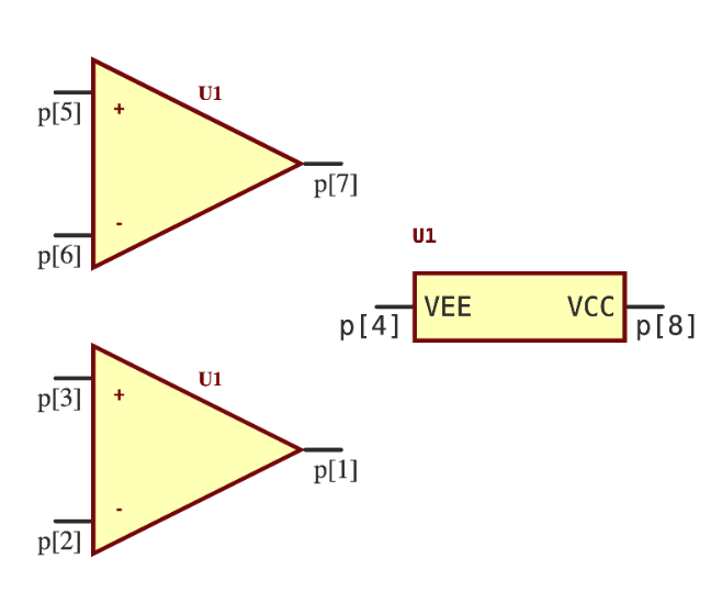
Multi-part Symbols
It is often useful to create symbols that have multiple constituent parts. For example, a dual operational
amplifier like the LM358LV contains two independent operational
amplifiers. JITX provides multi-part symbol support via the unit statement.
Unit Statement Example
Complete design example for multi-part symbols
public defstruct OpAmpBank :
  in+:JITXObject
  in-:JITXObject
  out:JITXObject

public defn make-multi-opamp-symbol (banks:Seqable<OpAmpBank>, VCC:Pin, VEE:Pin) :
  inside pcb-component:
    symbol :
      val psym = ocdb/utils/symbols/power-supply-sym
      unit(0) = psym(VCC => psym.vs+, VEE => psym.vs-)
      for (bank in banks, i in 1 to false) do :
        val sym = ocdb/utils/symbols/multi-op-amp-sym
        unit(i) = sym(
          in+(bank) => sym.vi+,
          in-(bank) => sym.vi-,
          out(bank) => sym.vo
        )
Notice that the unit statement takes a single Int argument as the index into the multi-part symbol array. You can then assign any symbol with the = assignment operator.
; Example use `make-multi-opamp-symbol`
;
pcb-component DualOpAmp:
  pin VCC
  pin VEE

  pin in1+
  pin in1-
  pin out1

  pin in2+
  pin in2-
  pin out2

  ...
  val banks = [
    OpAmpBank(in1+, in1-, out1),
    OpAmpBank(in2+, in2-, out2)
  ]
  make-multi-opamp-symbol(banks, VCC, VEE)
When invoked, this results in a component with 3 parts: a sub-part symbol for the power rails and 2 sub-parts for the op-amp symbols.
Complete listing for Multi-part Symbol Example
; Generated by JITX 2.20.0
#use-added-syntax(jitx)
defpackage main :
  import core
  import jitx
  import jitx/commands

; Define the shape/size of the board
val board-shape = RoundedRectangle(30.0, 18.5, 0.25)

public defstruct OpAmpBank :
  in+:JITXObject
  in-:JITXObject
  out:JITXObject

public defn make-multi-opamp-symbol (banks:Seqable<OpAmpBank>, VCC:Pin, VEE:Pin) :
  inside pcb-component:
    symbol :
      val psym = ocdb/utils/symbols/power-supply-sym
      unit(0) = psym(VCC => psym.vs+, VEE => psym.vs-)
      for (bank in banks, i in 1 to false) do :
        val sym = ocdb/utils/symbols/multi-op-amp-sym
        unit(i) = sym(
          in+(bank) => sym.vi+,
          in-(bank) => sym.vi-,
          out(bank) => sym.vo
        )

pcb-component DualOpAmp :
  pin VCC
  pin VEE

  pin in1+
  pin in1-
  pin out1

  pin in2+
  pin in2-
  pin out2

  val banks = [
    OpAmpBank(in1+, in1-, out1),
    OpAmpBank(in2+, in2-, out2)
  ]
  make-multi-opamp-symbol(banks, VCC, VEE)
  val soic = ocdb/utils/landpatterns/soic127p-landpattern(8)
  landpattern = soic(
    VCC => soic.p[8], VEE => soic.p[4],
    out1 => soic.p[1], in1- => soic.p[2], in1+ => soic.p[3],
    out2 => soic.p[7], in2- => soic.p[6], in2+ => soic.p[5],
  )

; Module to run as a design
pcb-module my-design :
  ; define some pins/ports
  pin gnd
  pin power-5v
  pin signal

  inst opa : DualOpAmp


defn setup-design (name:String, board:Board
                          --
                          rules:Rules = ocdb/utils/defaults/default-rules
                          vendors:Tuple<String|AuthorizedVendor> = ocdb/utils/design-vars/APPROVED-DISTRIBUTOR-LIST
                          quantity:Int = ocdb/utils/design-vars/DESIGN-QUANTITY) :
  set-current-design(name)
  set-board(board)
  set-rules(rules)
  set-bom-vendors(vendors)
  set-bom-design-quantity(quantity)

; Set the design name     - a directory with this name will be generated under the "designs" directory
;     the board           - a Board object
;     [optional] rules    - the PCB design rules (if not givn default rules will be used)
;     [optional] vendors  - Strings or AuthorizedVendors (if not give default vendors will be used)
;     [optional] quantity - Minimum stock quantity the vendor should carry (if not give default quantity will be used)
setup-design(
  "jitx-design",
  ocdb/utils/defaults/default-board(ocdb/manufacturers/stackups/jlcpcb-jlc2313, board-shape)
)

; Set the schematic sheet size
set-paper(ANSI-A)

; Set the top level module (the module to be compile into a schematic and PCB)
set-main-module(my-design)

; View the results
view-board()
view-schematic()
view-design-explorer()
Value Label
value-label can be used to change the value label of a component. value-label can also specify the location, size, orientation, etc. of the value label of a component.
You can set the value-label of a component by setting value-label(my-component) equal to a Text object. This Text object takes a string, text size, anchor location (N, E,S, or W), and the pose (loc) that specifies where to place the value label of the component.
Example usage
    ; name the test point,
    value-label(my-component) = Text("my-component-value", 1.0, W, loc(1.2, 0.0))
Enum Statements
pcb-enum is a way to store categorical variables.
Example
Right now we need to use a fully qualified name to define a new pcb-enum. So if we wanted an enum named:
Antenna
And we're defining it in a package named
defpackage ocdb/components/espressif/esp32-wroom-32
Then the enum needs to be defined as follows:
public pcb-enum ocdb/components/espressif/esp32-wroom-32/Antenna :
All together this is what it looks like to define and use a
pcb-enum:
defpackage ocdb/components/espressif/esp32-wroom-32:
...

public pcb-enum ocdb/components/espressif/esp32-wroom-32/Antenna :
  Integrated
  UMCX


  ; Using the pcb-enum as a type to define land pattern geometry
  pcb-landpattern esp32-wroom (antenna-type:Antenna) :
    switch(antenna-type):
      Integrated :
        package-y = 25.5
        offset = (25.5 - 19.2) / 2.0
      UMCX :
        package-y = 19.2
        offset = 0.0
Length of Enum
Get the length of an enum
When you create a new enum, called my-enum, Stanza (the language JITX uses) creates a new integer which represents the length of that enum, called my-enum-length.
Just add a -length to the end of any enum name to get its length.
Geometry Statements
Geometry statements are used to draw objects in JITX.
Shape
public deftype Shape <: Equalable & Hashable
| Statement | Description |
|---|---|
circle | Circle |
line | Line |
point | Point |
polygon | Polygon |
rectangle | Rectangle |
text | Text |
union | Union |
Circle
public defstruct Circle <: Shape :
  center: Point
  radius: Double with: (ensure => non-negative!)

public defn Circle (x:Double, y:Double, radius:Double) :
  Circle(Point(x,y), radius)

public defn Circle (anchor:Anchor, x:Double, y:Double, radius:Double) :
  val [vt, hr] = components(anchor)
  val x* = match(hr) :
    (hr:W) : x + radius
    (hr:C) : x
    (hr:E) : x - radius
  val y* = match(vt) :
    (vt:S) : y + radius
    (vt:C) : y
    (vt:N) : y - radius
  Circle(Point(x*,y*), radius)

public defn Circle (anchor:Anchor, radius:Double) :
  Circle(anchor, 0.0, 0.0, radius)

public defn Circle (radius:Double) :
  Circle(C, 0.0, 0.0, radius)
Circle(Point(1.0, 3.0), 1.5)
Circle(1.0, 3.0, 1.5)
Circle(C, 1.0, 3.0, 1.5)
Circle(C, 5.0)
Circle(5.0)
Line
public defstruct Line <: Shape  :
  width: Double with: (ensure => non-negative!)
  points: Tuple<Point> with: (ensure => min-length!(2))
with:
  constructor => #Line

public defn Line (width:Double, pts:Seqable<Shape|Seqable>) :
  val pts* = to-tuple(flatten-shapes(pts))
  ensure-points(pts*, "line")
  #Line(width, pts* as Tuple<Point>)
Line(0.15, [
  Point(2.0, 2.0),
  Point(-2.0, 2.0),
  Point(-2.0, -2.0),
  Point(2.0, -2.0)])
Point
public defstruct Point <: Shape :
  x: Double with: (updater => sub-x)
  y: Double with: (updater => sub-y)
Point(5.0, 1.0)
Polygon
public defstruct Polygon <: Shape :
  points: Tuple<Point> with: (ensure => min-length!(3))
with:
  constructor => #Polygon

public defn Polygon (pts:Seqable<Point|Seqable>) :
  val pts* = to-tuple(flatten-shapes(pts))
  ensure-points(pts*, "polygon")
  #Polygon(pts* as Tuple<Point>)
Polygon([
  Point(2.0, 2.0),
  Point(-2.0, 2.0),
  Point(-2.0, -2.0),
  Point(2.0, -2.0)])
Rectangle
public defstruct Rectangle <: Shape :
  width: Double with: (ensure => non-negative!)
  height: Double with: (ensure => non-negative!)
  pose: Pose

public defn Rectangle (w:Double, h:Double) :
  Rectangle(w, h, loc(0.0, 0.0))

public defn Rectangle (anchor:Anchor, w:Double, h:Double) :
  val [vt, hr] = components(anchor)
  val dx = match(hr) :
    (hr:W) : w / 2.0
    (hr:C) : 0.0
    (hr:E) : w / -2.0
  val dy = match(vt) :
    (vt:S) : h / 2.0
    (vt:C) : 0.0
    (vt:N) : h / -2.0
  Rectangle(w, h, loc(dx, dy))
Rectangle(2.0, 3.0, loc(0.0, 0.0))
Rectangle(2.0, 3.0)
Rectangle(C, 2.0, 3.0)
Text
How to create text on the silkscreen of your board and place that text anywhere you want.
The Text function supports placing an arbitrary string on the silkscreen of your board. You can speficy the font size, the anchoring location, and position of the text.
public defstruct Text <: Shape  :
  string: String with: (updater => sub-string)
  size: Double with: (ensure => non-negative!, updater => sub-size)
  anchor: Anchor with: (updater => sub-anchor)
  pose: Pose with: (updater => sub-pose)
anchor sets the anchor for the text object. i.e. is the origin centered (C), south (S), west (W), east (E), or north (N)? NE, NW, SE, SW are also options.
Text("Sample", 2.0, C, loc(1.0, 1.0))
Union
public defstruct Union <: Shape  :
  shapes: Tuple<Shape>
with:
  constructor => #Union

public defn Union (ss:Seqable<Shape|Seqable>) :
  val ss* = generate<Shape> :
    let loop (s:Shape|Seqable = ss) :
      match(s) :
        (s:Union) : do(yield, shapes(s))
        (s:Shape) : yield(s)
        (s:Seqable) : do(loop, s)
  if empty?(ss*) :
    fatal("Cannot form union from no shapes.")
  else :
    val s0 = next(ss*)
    if empty?(ss*) : s0
    else : #Union(to-tuple(cat([s0], ss*)))
Union([Circle(1.0), Rectangle(4.0, 0.5)])
Copper
The copper statement defines geometry on a specified copper layer of the board stackup.
This statement can be used in the following contexts:
- pcb-landpattern
- geom statements in a pcb-module
Signature
copper(<LAYER-INDEX>) = <Shape>
<LAYER-INDEX>- This expects a LayerIndex instance to select which copper layer to apply the created geometry.<Shape>- The geometric Shape to create in this copper layer.
Usage
That are two contexts in which the copper statement can be used. In each context, the usage is slightly different.
Land Pattern Context
In the pcb-landpattern context, the copper statement can be used standalone. This statement is used to create copper structures like an antenna in a landpattern. For example, see the ant-2GHz4-inverted-f-geom land pattern - here is an excerpt:
pcb-landpattern ant-2GHz4-inverted-f-geom :

  pad launch : smd-pad(0.5, 0.5) at loc(0.0, 0.25)
  pad gnd : smd-pad(0.9, 0.5) at loc(-2.1, 0.25)

  copper(LayerIndex(0)) = Line(0.5, [Point(-2.1, 5.15), Point(2.2, 5.15), Point(2.2, 2.51),
                                Point(4.7, 2.51),  Point(4.7, 5.15), Point(6.9, 5.15),
                                Point(6.9, 2.51),  Point(9.4, 2.51), Point(9.4, 5.15),
                                Point(11.6, 5.15), Point(11.6, 0.96)])
  copper(LayerIndex(0)) = Line(0.5, [Point(0.0, 0.0),   Point(0.0, 5.15)])
  copper(LayerIndex(0)) = Rectangle(0.9, 5.4, loc(-2.1, 2.7))
  ...
This will generate a shape that looks like this:
In the following image the 2nd and 3rd copper statements are drawn in a different color to show their position in relation to the pads of this landpattern:
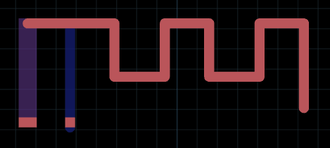
Geom/Module Context
In the pcb-module context, the copper statement can be used from within a geom statement. The geom statement provides the net to which this copper geometry will be assigned. The most common usage of this statement is defining ground planes or similar geometry with explicit shapes:
val board-shape = Rectangle(30.0, 40.0)

pcb-module top-level:
  ...

  geom(GND):
    val sh = offset{_, -1.0} $ RoundedRectangle(30.0, 10.0, 3.0)
    copper(LayerIndex(0, Bottom)) = loc(0.0, -15.0) * sh
Notice the use of offset to shrink the RoundedRectangle shape by 1mm. The loc function is used to transform the shrunken shape into position in the lower half of the PCB.
Constructs a shape on the bottom layer with geometry like this:
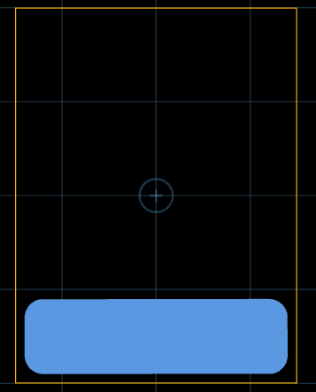
Syntax
geom(my-net):
  copper(LayerIndex(0)) = Circle(0.0, 15.0, 1.0)
  copper(LayerIndex(1)) = Line(1.0, [Point(0.0, -5.0) Point(5.0, -5.0)])
Description
copper(LayerIndex(0)) = Circle(0.0, 15.0, 1.0)Create a copper circle at (x,y) = (0,15mm) of radius 1mm. You can use any Shape with thecopperstatement.copper(LayerIndex(1)) = Line(1.0, [Point(0.0, -5.0) Point(5.0, -5.0)])Create a 1mm wide copper line (results in a trace) on the 2nd copper layer from the top.
Copper Pour
copper-pour is an ESIR statement for creating a filled outline on a copper-layer of our board. It gets exported to a plane in our CAD file.
Syntax
geom(my-net) :
  copper-pour(LayerIndex(0), isolate = 0.1) = Circle(0.0, 15.0, 1.0)
  copper-pour(LayerIndex(1), isolate = 0.1, rank = 1) = Rectangle(5.0, 5.0)
  copper-pour(LayerIndex(1), isolate = 0.1, rank = 1, orphans = true) = Rectangle(5.0, 5.0)
Description
copper-pour(LayerIndex(0), isolate = 0.1) = Circle(0.0, 15.0, 1.0)Create a circularcopper-pouron the top layer with 0.1mm geometric clearance/isolation.isolateis a required parameter for copper-pours. You can use any Shape with thecopper-pourstatement.copper-pour(LayerIndex(1), isolate = 0.1, rank = 1) = Rectangle(5.0, 5.0)Create a rectangular copper-pour on the second layer form the top, with 0.1mm clearance, and rank 1. Rank is an optional parameter that increases the priority of the pour - a higher-ranked pour fills before a lower ranked one.copper-pour(LayerIndex(1), isolate = 0.1, rank = 1, orphans = true) = ``Rectangle(5.0, 5.0)Similar to the previous command, but enable orphaned islands of copper to exist in the pour.
Place - how to place a component or module in JITX
In JITX, we can programmatically place components or modules on our board with a single line of code.
First, we specific place and the component that we want to place. Then we specify the location. Finally, we specifiy if we want to place it on the top or bottom.
Example placement
inst c : my-component
place(c) at loc(2.0, 3.0) on Top
loc
The loc statement is for placement in JITX. It creates an object describing translation and rotations that can be used to create goemetric constraints.
loc statements can be multiplied together (i.e. the transforms can be composed) and used to create trees of kinematic constraints.
pcb-landpatterns and pcb-modules have a right-handed coordinate system with origin at loc(0.0, 0.0, 0.0). Items you place in that coordinate frame will move together. e.g. you can move a land-pattern and all the pads stay in the same relative positions. You can place components in a module, and the relative positions of those components will remain fixed when you place the module.
Syntax
loc(1.0, 5.0)
loc(2.0, 3.0, 90.0)
loc(0.0, (- 3.0), (- 90.0)) on Bottom
loc(2.0, 3.0) on Top (relative-to proc)

pad p[0] : smd-pad(2.0, 1.0) at loc(0.0, 0.0, 90.0) * loc(2.0, 3.0)
pad p[1] : smd-pad(5.0, 1.0) at loc(2.0, 3.0) * loc(0.0, 0.0, 90.0)

inst c : my-component
place(c) at loc(2.0, 3.0) on Top
Description
loc(1.0, 5.0)Create a pose of (x,y) = (1.0mm, 5.0mm)loc(2.0, 3.0, 90.0)Create a pose of (x,y, theta) = (1.0mm, 5.0mm, 90 degrees)loc(2.0, 3.0, (- 90.0)) on TopCreate a pose of (x,y, theta) = (1.0mm, 5.0mm, -90 degrees), specifying that the component is on Top of the board.loc(0.0, (- 3.0), (- 90.0)) on BottomCreate a pose of (x,y, theta) = (0.0mm, -3.0mm, -90 degrees), specifying that the component is on the Bottom of the board.loc(2.0, 3.0) on Top (relative-to proc)Create a pose of (x,y) = (2.0mm, 3.0), defined from the origin of an instance named 'proc'. This is a relative constraint.
pad p[0] : smd-pad(2.0, 1.0) at loc(0.0, 0.0, 90.0) * loc(2.0, 3.0)
pad p[1] : smd-pad(5.0, 1.0) at loc(2.0, 3.0) * loc(0.0, 0.0, 90.0)
These statements create and place two pads at locations found by composing several poses together. The ordering of poses matters when you are composing them.
The pose loc(0.0, 0.0, 90.0) * loc(2.0, 3.0) first rotates the coordinate system by 90 degrees, and then translates it by (x,y) = (2.0mm, 3.0mm) in the new frame, so that the final pose is (x,y,theta) = (-3.0, 2.0, 90.0)
The pose loc(2.0, 3.0) * loc(0.0, 0.0, 90.0) first translates by (x,y) = (2.0mm, 3.0mm), then rotates the coordinate system by 90 degrees, so that the final pose is (x,y,theta) = (2.0, 3.0, 90.0). Here is the resulting pad geometry (origin of the land pattern is the blue cross):
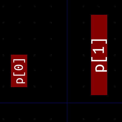
  inst c : my-component
  place(c) at loc(2.0, 3.0) on Top
Via [Deprecated]
The via statement defines a multi-layer via in a landpattern or the board according to the stackup.
This statement can be used in the following contexts:
- pcb-landpattern
- geom statements in a pcb-module
Signature
  via(<VIA-DEF>) at <Point>
  via(<VIA-DEF>, "Key-1" => "Value-1", ... ) at <Point>

  ; Deprecated Form
  via(
    <LayerIndex-1>, <LayerIndex-2>,
    type = <ViaType>
    radius = <Double>
    hole-radius = <Double>
    properties =  [ "Key-1" => "Value-1", ... ]
    ) at <Point>
- Required Parameters
<VIA-DEF- pcb-via definition for constructing the via.<LayerIndex-*>- In the deprecated form, a start and end layer for the via definition must be supplied as the first two arguments. These arguments must be LayerIndex instances.radius- Set the via copper land radius in mmhole-radius- Set the radius of the via hole in mm<Point>- This is expected to be aPointinstance that defines the location of the constructed via in the current context's coordinate frame.
- Optional Parameters
type- Sets the type of via as one ofTHVia|MicroVia|BlindVia. The default value isTHVia.properties- Set ofKeyValue<String, String>pairs for additional properties to set."Key-1" => "Value-1"- Set ofKeyValue<String, String>pairs for additional properties to set.
Usage
This statement is primarily a tool to help the importer successfully bring landpattern definitions from legacy CAD tools like Altium or Kicad.
Land Pattern Context
pcb-via default-via :
  name = "Default TH"
  start = LayerIndex(0, Top)
  stop = LayerIndex(0, Bottom)
  diameter = 0.6
  hole-diameter = 0.3
  type = MechanicalDrill

pcb-landpattern test:
  ...
  via(default-via) at Point(1.0, 2.0)
From the pcb-landpattern context, the via statement can be used directly.
The major ramification is that vias defined with this statement don't connect to nets. We suggest that you do not use this statement when designing PCB landpatterns.
When you encounter this statement in an imported PCB landpattern, you should remove this definition and place vias manually in the board visualization tool.
Geom/Module Context
In the pcb-module context, the via statement can be used from within a geom statement. The geom statement provides the net to which this via will be assigned.
pcb-module test-mod:
  ...
  geom(my-net):
    via(default-via) at Point(1.0, 2.0)

    via(LayerIndex(0), LayerIndex(0, Bottom),
        radius = 0.3, hole-radius = 0.125)
        at Point(0.0, 0.0)

    via(LayerIndex(1), LayerIndex(2),
        radius = 0.3, hole-radius = 0.125,
        type = BlindVia)
        at Point(1.0, 0.0)

    via(LayerIndex(0), LayerIndex(1),
        radius = 0.1, hole-radius = 0.05,
        type = MicroVia)
        at Point(2.0, 0.0)
The last three examples are the deprecated form of this statement. The better way to use the via statement is to use pcb-via definitions and use them by reference.
Land Patterns
A pcb-landpattern statement defines the pads and associated geometry for the interface between an electrical component and the PCB. This is also known as a footprint, package, or land-pattern.
Signature
pcb-landpattern lp-name (arg1:Type1, ...) :
  name = <String|False>
  description = <String|False>

  external-names = <Tuple<String>|False>
  model3d = <Model3D>

  <PAD-1>
  ...
  <LAYER-1>
  ...
The expression name lp-name uniquely identifies this via definition
in the current context.
The argument list (arg1:Type1, ...) is optional and provides a means of
constructing parameterized landpattern definitions.
name- This name is used in the UI as a more user friendly name. If this string is not provided then thelp-nameexpression is used as the landpattern's name.description- This string is defining more meta-data for the landpattern.external-names- Optional tuple ofStringinstances of alternate names for this landpattern.model3d- The model3d statement expects aModel3Dinstance to define the data and pose for the 3D model of this component.<PAD-1>- A pad statement defines a electrical connection interface point.- The landpattern expects zero or more pads.
- The pad reference is part of the
pcb-symbol -> pcb-landpatternmapping in the pcb-component definition.
<LAYER-1>- A layer() statement defines what geometry to create on the non-copper layers.
Usage
Here is a typical land-pattern example, featuring a 3-pin SOT-23 :
pcb-landpattern Static-SOT23 :

  val x0 = 1.0  ; Lead-Span spacing
  val y0 = 0.95 ; Pitch
  ; Pad Definitions
  val pdef = smd-pad(0.8, 0.5)
  pad p[1] : pdef at loc((- x0), y0)
  pad p[2] : pdef at loc((- x0), (- y0))
  pad p[3] : pdef at loc(x0, 0.0)

  ; Non-Copper Geometry
  layer(Courtyard(Top)) = Rectangle(3.3, 3.0)
  layer(Silkscreen("f-silk", Top)) = LineRectangle(3.3, 3.0)
  ; Reference Designator Helper Function
  ref-label()
If we attempt to visualize this landpattern:
view(Static-SOT23)
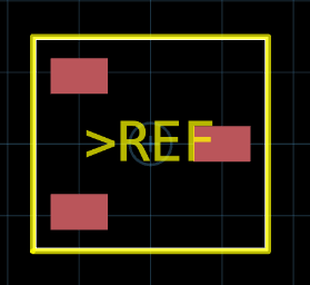
In this definition, notice that you can use standard stanza syntax like defining immutable values (eg, val x0 = -0.95). This can make constructing landpatterns easier because we can use arithmetic directly in the land-pattern definition.
What the >REF?
The
>REFtext in the silkscreen might be a bit jarring at first, but keep in mind that we are defining the land pattern - this isn't what is going to be in the resultant board. The>REFwill get replaced by a reference designator and that designator will be positioned automatically.
Pad Definitions
The definition for smd-pad can be found in OCDB. This defines a typical surface mount pad. There are multiple ways of invoking smd-pad:
; Originating Definitions
pcb-pad smd-pad (copper-layer:Shape, solder-mask-layer:Shape|False, paste-layer:Shape) :
  ...

; Polymorphic Functions
defn smd-pad (s:Shape) -> Pad
defn smd-pad (anchor:Anchor, width:Double, height:Double) -> Pad
defn smd-pad (d:Dims) -> Pad
defn smd-pad (width:Double, height:Double) -> Pad
The top definition is the base pcb-pad definition and then the following functions are all different ways to create that originating definition. These are polymorphic functions.
Poly-Wut? - Polymorphism is a fancy way of saying that the compiler is going take whatever args you give for a particular function and do its level best to call the right function to give you the result you want. It may not be able to satisfy every request. This may be due to a lack of a definition that supports that modality. Or it may be due to an ambiguity in the definition or the invocation.
Big Picture - The
smd-padsymbol encodes the core idea - eg, This function returns a surface mount pad definition. All of the polymorphic versions of this function must adhere to that core idea.
Layer Content
The next section of the pcb-landpattern definition is the non-copper layer() statements. This includes the courtyard, silkscreen, forbid/keepout regions, and any other pertinent content you might wish to include in the land-pattern.
The ref-label function is a generator. Here is an excerpt from the ref-label definitions:
defn ref-label (pose:Pose, anchor:Anchor) :
  inside pcb-landpattern:
    val min-height = clearance(current-rules(), MinSilkscreenTextHeight)
    layer(Silkscreen("values", Top)) = Text(">REF", min-height, anchor, pose)

defn ref-label () :
  ref-label(loc(0.0, 0.0), C)
The inside pcb-landpattern statement is what makes this function a generator. The lines inside this statement effectively get copied in to the parent context (in this case, the Static-SOT23 land-pattern definition).
The idea is that inserting a reference designator label into a pcb-landpattern definition is a pretty common activity. Copying and pasting this into every pcb-landpattern definition would get annoying fast. It also would be pretty significant violation of the "Don't Repeat Yourself" principle. The ref-label generator allows us to inject content into the parent context without necessarily knowing when and where it will get used.
Arguments to a Land Pattern
Arguments to a landpattern can be an effective way to construct highly reusable land patterns:
pcb-landpattern header (num-pins:Int, pitch:Double = 2.54):
  val pdef = pth-pad(0.9, 1.15)
  for i in 1 through num-pins do:
    pad p[i] : pdef at loc(to-double(i  - 1) * pitch, 0.0)
  ...
These arguments allow us to construct an N-pin through-hole single-row header and customize its pitch. The pitch argument has a default value making it optional.
You can find a more advanced example of pcb-landpattern with arguments here.
Statements
Here is the list of all of the statements you can use in a pcb-landpattern :
| Statement | Description |
|---|---|
description | Description for the land pattern |
external-names | Define common names for the land pattern |
layers | Define shapes on layers like SolderMask |
name | Name of the land pattern |
pad | Creates pads you can connect to |
model3d | Associate a 3D model with a landpattern |
copper | Construct unassociated copper geometry in the landpattern |
via | Construct unassociated via placements in the landpattern |
Copper
The copper statement defines geometry on a specified copper layer of the board stackup.
This statement can be used in the following contexts:
- pcb-landpattern
- geom statements in a pcb-module
Signature
copper(<LAYER-INDEX>) = <Shape>
<LAYER-INDEX>- This expects a LayerIndex instance to select which copper layer to apply the created geometry.<Shape>- The geometric Shape to create in this copper layer.
Usage
That are two contexts in which the copper statement can be used. In each context, the usage is slightly different.
Land Pattern Context
In the pcb-landpattern context, the copper statement can be used standalone. This statement is used to create copper structures like an antenna in a landpattern. For example, see the ant-2GHz4-inverted-f-geom land pattern - here is an excerpt:
pcb-landpattern ant-2GHz4-inverted-f-geom :

  pad launch : smd-pad(0.5, 0.5) at loc(0.0, 0.25)
  pad gnd : smd-pad(0.9, 0.5) at loc(-2.1, 0.25)

  copper(LayerIndex(0)) = Line(0.5, [Point(-2.1, 5.15), Point(2.2, 5.15), Point(2.2, 2.51),
                                Point(4.7, 2.51),  Point(4.7, 5.15), Point(6.9, 5.15),
                                Point(6.9, 2.51),  Point(9.4, 2.51), Point(9.4, 5.15),
                                Point(11.6, 5.15), Point(11.6, 0.96)])
  copper(LayerIndex(0)) = Line(0.5, [Point(0.0, 0.0),   Point(0.0, 5.15)])
  copper(LayerIndex(0)) = Rectangle(0.9, 5.4, loc(-2.1, 2.7))
  ...
This will generate a shape that looks like this:

In the following image the 2nd and 3rd copper statements are drawn in a different color to show their position in relation to the pads of this landpattern:

Geom/Module Context
In the pcb-module context, the copper statement can be used from within a geom statement. The geom statement provides the net to which this copper geometry will be assigned. The most common usage of this statement is defining ground planes or similar geometry with explicit shapes:
val board-shape = Rectangle(30.0, 40.0)

pcb-module top-level:
  ...

  geom(GND):
    val sh = offset{_, -1.0} $ RoundedRectangle(30.0, 10.0, 3.0)
    copper(LayerIndex(0, Bottom)) = loc(0.0, -15.0) * sh
Notice the use of offset to shrink the RoundedRectangle shape by 1mm. The loc function is used to transform the shrunken shape into position in the lower half of the PCB.
Constructs a shape on the bottom layer with geometry like this:

Syntax
geom(my-net):
  copper(LayerIndex(0)) = Circle(0.0, 15.0, 1.0)
  copper(LayerIndex(1)) = Line(1.0, [Point(0.0, -5.0) Point(5.0, -5.0)])
Description
copper(LayerIndex(0)) = Circle(0.0, 15.0, 1.0)Create a copper circle at (x,y) = (0,15mm) of radius 1mm. You can use any Shape with thecopperstatement.copper(LayerIndex(1)) = Line(1.0, [Point(0.0, -5.0) Point(5.0, -5.0)])Create a 1mm wide copper line (results in a trace) on the 2nd copper layer from the top.
Description
description is the optional descriptive field of a JITX object. Use it to store a description of the object for human designers reading JITX, and to make the object easier to find via text search. This description also shows up in the UI, such as the design explorer, to provide more insight into particular components and modules in the design.
Signature
description = <String>
Examples
; We can use string literals to describe a particular component.
pcb-component analog-devices-ADM7150 :
  description = "800 mA Ultralow Noise, High PSRR, RF Linear Regulator"

; We can use string formatting to construct descriptions based on variables
;   or arguments to a JITX Definition
pcb-module band-pass-filter (high-cut:Double, low-cut:Double) :
  description = to-string("Band-pass Filter - Highpass = %_ Hz and Lowpass = %_ Hz.")
External Names
external-names is an optional field in a pcb-landpattern to allow us to match the land pattern with parts found at component vendors.
Syntax
external-names = (["0402"])
external-names = (["0402" "0402-01005"])
Description
external-names = (["0402"])Indicate this land pattern matches "0402"-sized SMD componentsexternal-names = (["0402" "0402-01005"])Indicate this land pattern matches "0402" and "0402-01005"-sized SMD components. Each additional string is another alias.
Layer
The layer statement is used to create geometry on the non-copper layers of a circuit board. The layer() statement is valid in the following contexts:
Signature
layer(<LayerSpecifier>) = <Shape>
<LayerSpecifier>- A LayerSpecifier instance that identifies which non-copper layer to apply the provided geometry to.<Shape>- AShapeinstance that defines the geometry that will be created on the specified layer.
Usage
The most common usage of the layer() statement is in pcb-landpattern:
pcb-landpattern diode-lp :
  pad c : smd-pad(0.4, 0.75) at loc(-1.25, 0.0) on Top
  pad a : smd-pad(0.4, 0.75) at loc(1.25, 0.0) on Top

  layer(Silkscreen("body", Top)) = LineRectangle(1.8, 1.0)
  layer(Silkscreen("body", Top)) = Line(0.1, [Point(-0.70, -0.5), Point(-0.70, 0.5)])
  layer(Courtyard(Top)) = Rectangle(3.2, 2.0)

  layer(ForbidCopper(LayerIndex(0))) = Rectangle(2.0, 1.0)
This will construct a landpattern that looks like this:

Notice the silkscreen in yellow with cathode marker. The blue box is the ForbidCopper layer on the Top Layer. Red is the top copper pads for the cathode c and anode a.
The white bounding rectangle is the Courtyard layer.
See LayerSpecifier for more information about specific layers.
Cutouts
When constructing cutouts in the board layout, your best bet is to use a solid region as opposed to a line. A line can confuse the routing engine into thinking that there are two physically separate regions where copper can be placed.
Consider a USB connector part, U231-096N-3BLRT06-SS, Jing Extension of the Electronic Co.
Here is an excerpt from the datasheet:

If we draw the cutout with a line, as shown in the datasheet, we get this:
pcb-landpattern USB-conn:
  ...

  layer(Cutout()) = Line(0.254, [Point(-7.300, -7.650), Point(-8.450, -7.650)])
  layer(Cutout()) = Polyline(0.254, [
    Point(6.850, 4.650)
    Point(6.850, -7.650)
    Point(8.450, -7.650)])
  layer(Cutout()) = Polyline(0.254, [
    Point(-6.850, 4.650)
    Point(-6.850, -7.650)
    Point(-7.300, -7.650)])
  layer(Cutout()) = Line(0.254, [Point(-6.850, 4.650), Point(6.850, 4.650)])

The cutout line is in gold color. Notice that the ground layer (blue) copper is present on both sides of the cut line with some margin in between. The routing engine basically thinks that the cutout is just the line. If we were making a slot - that would probably be reasonable. But for this case, we want the hole region between the cutout line and the board edge (red) to be a cutout region.
The right way is to use a Rectangle or Polygon solid geometry:
pcb-landpattern USB-conn :
  ...

  layer(Cutout()) = Polygon([
    Point(-6.850, 4.650), Point(6.850, 4.650),
    Point(6.850, -7.650), Point(-6.850, -7.65),
  ])
  layer(Cutout()) = Circle(Point(-6.85 + 0.5, 4.65), 0.5)
  layer(Cutout()) = Circle(Point(6.85 - 0.5, 4.65), 0.5)

Notice that the cutout region fills the entire connector region and the blue ground plane is not present in the cutout region.
Name
name is the optional name field of a JITX object. Use it to store a descriptive name as a String. This name will often be used in the UI in place of the object's expression name for better readability.
Signature
name = <String>
Usage
Literal String Names
pcb-component component :
  name = "ADM7150"

pcb-module band-pass-filter :
  name = "Band-pass filter"
The examples name = "ADM7150" and name = "Band-pass filter" use a String liternal for the name.
Formatted Strings
pcb-pad smd-pad (anchor:Anchor, w:Double, h:Double) :
  name = to-string("%_x%_ %_ SMD Pad" % [w,h,anchor])

pcb-landpattern test-lp:
  pad p[1] : smd-pad(C, 0.6, 0.7) at loc(x0,y0)
We can also construct strings using formatting routes and parameter arguments for a particular definition. In this example, the constructed smd-pad name property would be 0.6x0.7 C SMD Pad
Pad
pad statement defines an electrical connection point in a pcb-landpattern. A pad is an object that you can associate with a component pin.
Signature
pad <REF> : <DEF> at <POSE>
pad <REF> : <DEF> at <POSE> on <SIDE>
<REF>- The pad's ref name in thepcb-landpatterncontext. Common ref names arep[1],p[2], etc. Notice the index starting at one instead of zero.<DEF>- A reference to apcb-paddefinition. This will define the geometry and configuration of this specific pad in the land-pattern.<POSE>- APoseinstance that transforms thepcb-paddefinition into the appropriate location in thepcb-landpatternframe of reference.<SIDE>- ASideinstance ofTop|Bottomthat indicates whether this pad is located on the top or bottom side of the board. The default side if theon <SIDE>expression is not provided isTop.
Usage
The pad statement is used as part of a pcb-landpattern definition to define the electrical connection points between the PCB and a component. There are typically multiple pad statements in a pcb-landpattern definition.
Reference Examples
When defining the pad reference, we can use any dot notation or array indexing feature:
pad a : square-pad at loc(0.0, 0.0)
pad p[0] : smd-pad(0.5, 0.5) at loc(5.0, 0.0)

pad dp.P : pth-pad(0.5, 0.9) at loc(-2.0, 0.0)
pad dp.N : pth-pad(0.5, 0.9) at loc(2.0, 0.0)
The dot notation example dp.P and dp.N is particular useful when attempting to create a pcb-landpattern that interfaces to a diff-pair bundle component port. See pcb-component for more information.
Constructing Pads in Loops
We can use typical stanza for-loop constructions inside the pcb-landpattern to make it easier to build many pins:
val pdef = smd-pad(0.8, 0.3)
for i in 1 through num-pins do:
  val pose = loc(to-double(i) * 1.27, 0.0)
  pad p[i] : pdef at pose
Notice the use of 1 through num-pins as the sequence generator. If num-pins = 4 - then this will construct the sequence [1, 2, 3, 4] for a one-based index.
Using on <SIDE>
When constructing a board edge connector (like a PCIe card), we often need to place pads on both side of the board:
pcb-landpattern Card-Edge (num-pins:Int):
  val pdef = smd-pad(0.4, 1.6)
  val pitch = 1.2
  for i in 1 through num-pins do:
    pad A[i] : pdef at loc( to-double(i) * pitch, 0.0) on Top
    pad B[i] : pdef at loc( to-double(i) * pitch, 0.0) on Bottom
Careful with Ref Names
It is an error to create two pads with the same reference. For example, this case:
pcb-landpattern diode-lp :
  pad c : smd-pad(0.4, 0.75) at loc(-1.25, 0.0) on Top
  pad a : smd-pad(0.4, 0.75) at loc(1.25, 0.0) on Top
  pad a : smd-pad(0.4, 0.75) at loc(1.25, 2.0) on Top
Notice the duplicate a pad. This will throw an exception when the design is run:
Uncaught Exception: StmtTable adding duplicate record - key: a ...
Programmatically Generated Ref Names
Often times it can be useful to programmatically generate a ref name for a pad. To do this we need to use a special syntax to force the compiler to interpret a variable as a reference by value instead of a symbol:
val prefix = Ref("RP")
pad (prefix)[4] : bga-pad(1.0) at loc(1.0, 0.0)
This will construct a pad with ref RP[4]. Notice how in this case the prefix value is wrapped in parenthesis (). This forces the compiler to interpret the value of prefix as the reference. Compare this to the case where there is no ():
val prefix = Ref("RP")
pad prefix[4] : bga-pad(1.0) at loc(1.0, 0.0)
In this case the pad would have the literal reference name prefix[4].
Via [Deprecated]
The via statement defines a multi-layer via in a landpattern or the board according to the stackup.
This statement can be used in the following contexts:
- pcb-landpattern
- geom statements in a pcb-module
Signature
  via(<VIA-DEF>) at <Point>
  via(<VIA-DEF>, "Key-1" => "Value-1", ... ) at <Point>

  ; Deprecated Form
  via(
    <LayerIndex-1>, <LayerIndex-2>,
    type = <ViaType>
    radius = <Double>
    hole-radius = <Double>
    properties =  [ "Key-1" => "Value-1", ... ]
    ) at <Point>
- Required Parameters
<VIA-DEF- pcb-via definition for constructing the via.<LayerIndex-*>- In the deprecated form, a start and end layer for the via definition must be supplied as the first two arguments. These arguments must be LayerIndex instances.radius- Set the via copper land radius in mmhole-radius- Set the radius of the via hole in mm<Point>- This is expected to be aPointinstance that defines the location of the constructed via in the current context's coordinate frame.
- Optional Parameters
type- Sets the type of via as one ofTHVia|MicroVia|BlindVia. The default value isTHVia.properties- Set ofKeyValue<String, String>pairs for additional properties to set."Key-1" => "Value-1"- Set ofKeyValue<String, String>pairs for additional properties to set.
Usage
This statement is primarily a tool to help the importer successfully bring landpattern definitions from legacy CAD tools like Altium or Kicad.
Land Pattern Context
pcb-via default-via :
  name = "Default TH"
  start = LayerIndex(0, Top)
  stop = LayerIndex(0, Bottom)
  diameter = 0.6
  hole-diameter = 0.3
  type = MechanicalDrill

pcb-landpattern test:
  ...
  via(default-via) at Point(1.0, 2.0)
From the pcb-landpattern context, the via statement can be used directly.
The major ramification is that vias defined with this statement don't connect to nets. We suggest that you do not use this statement when designing PCB landpatterns.
When you encounter this statement in an imported PCB landpattern, you should remove this definition and place vias manually in the board visualization tool.
Geom/Module Context
In the pcb-module context, the via statement can be used from within a geom statement. The geom statement provides the net to which this via will be assigned.
pcb-module test-mod:
  ...
  geom(my-net):
    via(default-via) at Point(1.0, 2.0)

    via(LayerIndex(0), LayerIndex(0, Bottom),
        radius = 0.3, hole-radius = 0.125)
        at Point(0.0, 0.0)

    via(LayerIndex(1), LayerIndex(2),
        radius = 0.3, hole-radius = 0.125,
        type = BlindVia)
        at Point(1.0, 0.0)

    via(LayerIndex(0), LayerIndex(1),
        radius = 0.1, hole-radius = 0.05,
        type = MicroVia)
        at Point(2.0, 0.0)
The last three examples are the deprecated form of this statement. The better way to use the via statement is to use pcb-via definitions and use them by reference.
model3d
model3d is a JITX statement that defines a 3D model associated with a pcb-landpattern definition.
Syntax
; inside pcb-landpattern :
model3d = Model3D(filename, position, scale, rotation) where :
  val filename = "my-3d-model.wrl"
  val position = Vec3D(0.0, 0.0, 0.0)
  val scale    = Vec3D(0.0, 0.0, 0.0)
  val rotation = Vec3D(0.0, 0.0, 0.0)
Description
The model3d statement associates a 3D model with a pcb-landpattern. Models may be .stp, .step, or .wrl files. The arguments to Model3D are the name of the 3D model file, and 3D vectors for position/translation, scale, and rotation.
The filename argument may be a relative or absolute path. If it is relative, the resolved path will be relative to the directory of the source file that contains the statement. If it is started with ${PROJECT_ROOT} (e.g. ${PROJECT_ROOT}/3DModels/model.step), the resolved path will be relative to the project root directory.
For example :
  ;in project/landpatterns/landpattern.stanza
  ;...
  model3d = Model3D("../3DModels/model.step")
The resolved path will be project/3DModels/model.step.
During import, imported model files are placed in the imported design directory under <imported-design>/3d-models and model3d statements are generated automatically.
Landpattern with Arguments
After designing a few boards, it becomes apparent that while most SOT-23's are about the same, there are always some outliers. One manufacturer might claim a slightly different tolerance to another. This typically results in either a land-pattern that isn't necessarily tuned for each part (ie, one land pattern to rule them all) or a plurality of land patterns for each of those cases. Maintaining this library of land patterns quickly becomes a full-time job.
With the ability to write circuits-as-code, we open a new way to support dynamically generated land-patterns. The following is an excerpt from this complete example:
Note - This is a more complex example. But fear not stalwart electron herder, these examples will serve you well as you become more familiar with the JITX environment.
pcb-landpattern SOT-23 (pad-size:Dims, pad-grid:Dims, margin:Double = 0.2) :
  val x0 = x(pad-grid)
  val y0 = y(pad-grid)

  ; Pad Definitions
  val pdef = smd-pad(pad-size)
  pad p[1] : pdef at loc((- x0), y0)
  pad p[2] : pdef at loc((- x0), (- y0))
  pad p[3] : pdef at loc(x0, 0.0)

  ; Find the bounding box around all of the pads.
  val outline = bounds $ Union $ for pd in pads(self) seq:
    pose(pd) * pad-shape(pdef)

  ; Non-Copper Geometry
  val outline* = offset(outline, margin) as RoundedRectangle
  val courtyard = LineRectangle(width(outline*), height(outline*))
  layer(Courtyard(Top)) = courtyard
  layer(Silkscreen("f-silk", Top)) = courtyard

  ; Construct the Pin #1 marker in the silkscreen
  val r = 0.15
  val marker = loc((width(outline*) / -2.0) - (3.0 * r), y0)
  layer(Silkscreen("f-silk", Top)) = marker * Circle(2.0 * r)
  ; Reference Designator Helper Function
  ref-label()
If we attempt to visualize this landpattern, we should see:
view(SOT-23(Dims(0.8, 0.5), Dims(1.0, 0.95)))
You can still see the skeleton of the static SOT-23 implementation but we've added some new features:
- We've added some arguments to the
pcb-landpatterndefinition that allow us to create a SOT-23 landpattern to our exact specifications. - We compute the bounding rectangle for the pads so that we can construct courtyard and silkscreen outlines dynamically. This reduces the amount of magic numbers in our design.
- We add a "Pin 1" marker that is placed outside the silkscreen boundary.
Arguments
The arguments are encoded at the beginning of the definition as if this were a normal function definition:
pcb-landpattern SOT-23 (pad-size:Dims, pad-grid:Dims -- margin:Double = 0.2) :
  ...
The pad-size defines the width/height of the pads. The pad-grid defines the "Lead Span" (X) and "Pitch" (Y) of the constructed pads. These are both required arguments.
The margin is the extra space between the external boundary of the pads and the constructed courtyard/silkscreen outlines. This argument has a default value of 0.2 which means that it is optional argument.
Boundary Rectangle
The core functionality that makes this routine possible is the following line:
  ; Find the bounding box around all of the pads.
  val outline = bounds $ Union $ for pd in pads(self) seq:
    pose(pd) * pad-shape(pdef)
We can break this down into constituent pieces:
for pd in pads(self) seq:
This is a for-loop, like many we have seen before, but this one has something different at the end - a seq instead of a do. seq is an operating function. In particular, seq will convert all of the values returned by the body of this for-loop into a Sequence (iterator).
The pads function provides a sequence of LandPatternPad instances - one for each of the defined pad statements in the landpattern.
The body of the for-loop consists of:
pose(pd) * pad-shape(pdef)
This takes the shape from the pad definition pdef and then translates it according to the Pose of that pad instance. This translation is so that we don't end up with just 3 rectangles right on top of each other at the origin.
The resultant sequence from the for-loop is passed to the Union shape
constructor function via the Apply Operator, the $ operator.
The Union shape is method of constructing complex shapes. It constructs the geometric union as the name suggests.
The bounds function is similarly invoked via the apply operator. Note how the apply operator allows for chaining a sequence of functions on the output of the for-loop. The bounds function computes the axis-aligned bounding box around the Union shape of all the pads in the land pattern.
That outline result is a Rectangle shape that we can now use to construct our courtyard/silkscreen outline or correctly place the pin-1 marker for our component.
#use-added-syntax(jitx)
defpackage dynamic_landpatterns:
  import core
  import jitx
  import jitx/commands
  import ocdb/utils/landpatterns
  import ocdb/utils/box-symbol

doc: \<DOC>
Static Version
<DOC>
pcb-landpattern Static_SOT23 :

  val x0 = 1.0  ; Lead-Span spacing
  val y0 = 0.95 ; Pitch
  ; Pad Definitions
  val pdef = smd-pad(0.8, 0.5)
  pad p[1] : pdef at loc((- x0), y0)
  pad p[2] : pdef at loc((- x0), (- y0))
  pad p[3] : pdef at loc(x0, 0.0)

  ; Non-Copper Geometry
  layer(Courtyard(Top)) = Rectangle(3.3, 3.0)
  layer(Silkscreen("f-silk", Top)) = LineRectangle(3.3, 3.0)
  ; Reference Designator Helper Function
  ref-label()

doc: \<DOC>
Very Limited Bounding Region Calculation
<DOC>
defn bounds (sh:Union|Shape) -> Rectangle :

  val extrema = to-tuple $ for s in shapes(sh as Union) seq:
    match(s):
      (r:Rectangle):
        val w2 = width(r) / 2.0
        val h2 = height(r) / 2.0
        ; println("W: %_ H: %_ P: %_" % [w2, h2, pose(r)] )
        [pose(r) * Point(w2, h2), pose(r) * Point((- w2), (- h2))]
      (other):
        throw $ Exception("Unhandled Shape")

  val max-x = maximum $ for obj in extrema map:
    x(obj[0])
  val max-y = maximum $ for obj in extrema map:
    y(obj[0])
  val min-x = minimum $ for obj in extrema map:
    x(obj[1])
  val min-y = minimum $ for obj in extrema map:
    y(obj[1])

  val mid-x = (max-x + min-x) / 2.0
  val mid-y = (max-y + min-y) / 2.0
  val w = max-x - min-x
  val h = max-y - min-y
  Rectangle(w, h, loc(mid-x, mid-y))

doc: \<DOC>
Dynamic Version
<DOC>
pcb-landpattern SOT-23 (pad-size:Dims, pad-grid:Dims, margin:Double = 0.2) :
  val x0 = x(pad-grid)
  val y0 = y(pad-grid)

  ; Pad Definitions
  val pdef = smd-pad(pad-size)
  pad p[1] : pdef at loc((- x0), y0)
  pad p[2] : pdef at loc((- x0), (- y0))
  pad p[3] : pdef at loc(x0, 0.0)

  ; Find the bounding box around all of the pads.
  val outline = bounds $ Union $ for pd in pads(self) seq:
    pose(pd) * pad-shape(pdef)

  ; Non-Copper Geometry
  val outline* = offset(outline, margin) as RoundedRectangle
  val courtyard = LineRectangle(width(outline*), height(outline*))
  layer(Courtyard(Top)) = courtyard
  layer(Silkscreen("f-silk", Top)) = courtyard

  val r = 0.15
  val marker = loc((width(outline*) / -2.0) - (3.0 * r), y0)
  layer(Silkscreen("f-silk", Top)) = marker * Circle(2.0 * r)
  ; Reference Designator Helper Function
  ref-label()


; view(Static_SOT23)
view(SOT-23(Dims(0.8, 0.5), Dims(1.0, 0.95)))
Materials
A pcb-material definition represents a material in a pcb-stackup layer.
Signature
pcb-material mat-name (arg1:Type1, ...) :
  name = <String|False>
  description = <String|False>
  type = <MaterialType>

  material-name = <String|False>

  ; For Dielectric Materials
  dielectric-coefficient = <Double|False>
  loss-tangent = <Double|False>

  ; For Conductor Materials
  roughness = <Double|False>
The expression name mat-name uniquely identifies this stackup definition in the current context.
The argument list (arg1:Type1, ...) is optional and provides a means of
constructing parameterized material definitions.
- Required Parameters
type- There are two valid values forMaterialTypeConductorDielectric
- Optional Parameters
name- This name is used in the UI as a more user friendly name. If this string is not provided then themat-nameexpression is used as the stackup's name.description- This string is defining more meta-data for the material - such as manufacturer of this material.material-name- This string label is optional and used only for Kicad Import/Export.DielectricType Optional Parametersdielectric-coefficient- Relative Coefficient of Permittivity for this material. This value is a unit-less instance of typeDoubleand generally should be 1.0 or greater.loss-tangent- The Loss Tangent for this material. This value is a unit-less instance of typeDouble.
ConductorType Optional Parametersroughness- Surface Roughness of the conductor layer. This parameter effects the losses in RF circuits due to the skin effect. This value is in mm.
If you add roughness to a Dielectric type or a loss-tangent to a Conductor type, the JITX runtime will throw an error.
Example:
Uncaught Exception: Dielectrics can only have dielectric-coefficient and loss-tangent attributes.
Usage
The pcb-material statements create definitions that are primarily used by the pcb-stackup statement. These material definitions provide the properties of each material in the stackup.
Below is a trivial example for a 2-layer board:
pcb-material core-45 :
  type = Dielectric
  dielectric-coefficient = 4.5
  loss-tangent = 0.008

pcb-material soldermask :
  type = Dielectric
  dielectric-coefficient = 3.2
  loss-tangent = 0.012

pcb-material copper:
  type = Conductor

pcb-stackup simple-2-layer :
  name = "2-layer 1.6mm"
  layer(0.019, soldermask)
  layer(0.035, copper)
  layer(1.5, core-45)
  layer(0.035, copper)
  layer(0.019, soldermask)
Using Arguments
Often times, a family of prepreg materials will come in multiple different constructions. For example, see Isola 370HR. Here is an excerpt from their core data:
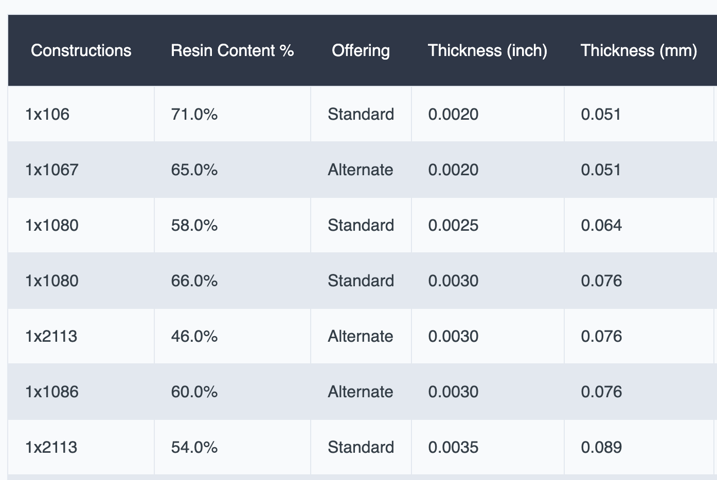
We might want to construct a pcb-material that allows us to label with these different features:
pcb-material isola-370HR (ply:String, Dk:Double, Df:Double) :
  name = to-string("Isola 370HR %_" % [ply])
  type = Dielectric
  dielectric-coefficient = Dk
  loss-tangent = Df

val isola-370hr-1080 = isola-370HR("1x1080", 4.04, 0.021)
This structure allows us to build a material spec for any
of the cores in the Isola catalog. The name for this material will be Isola 370HR 1x1080 which we can use in programmatically generated stackup tables.
Name
name is the optional name field of a JITX object. Use it to store a descriptive name as a String. This name will often be used in the UI in place of the object's expression name for better readability.
Signature
name = <String>
Usage
Literal String Names
pcb-component component :
  name = "ADM7150"

pcb-module band-pass-filter :
  name = "Band-pass filter"
The examples name = "ADM7150" and name = "Band-pass filter" use a String liternal for the name.
Formatted Strings
pcb-pad smd-pad (anchor:Anchor, w:Double, h:Double) :
  name = to-string("%_x%_ %_ SMD Pad" % [w,h,anchor])

pcb-landpattern test-lp:
  pad p[1] : smd-pad(C, 0.6, 0.7) at loc(x0,y0)
We can also construct strings using formatting routes and parameter arguments for a particular definition. In this example, the constructed smd-pad name property would be 0.6x0.7 C SMD Pad
Description
description is the optional descriptive field of a JITX object. Use it to store a description of the object for human designers reading JITX, and to make the object easier to find via text search. This description also shows up in the UI, such as the design explorer, to provide more insight into particular components and modules in the design.
Signature
description = <String>
Examples
; We can use string literals to describe a particular component.
pcb-component analog-devices-ADM7150 :
  description = "800 mA Ultralow Noise, High PSRR, RF Linear Regulator"

; We can use string formatting to construct descriptions based on variables
;   or arguments to a JITX Definition
pcb-module band-pass-filter (high-cut:Double, low-cut:Double) :
  description = to-string("Band-pass Filter - Highpass = %_ Hz and Lowpass = %_ Hz.")
Module Level Statements
A pcb-module definition represents a group of instances, their statuses, their nets, and layers or geoms in a design. Modules form the hierarchy of your design and can be instantiated, placed, and connected via nets.
Syntax
pcb-module my-module :
  port power : ocdb/bundles/power

  inst mcu        : components/manu/CoolCPU-123
  inst peripheral : components/manu/Awesome-Peripheral-456
  inst fuse       : components/manu/broken-fuse
  inst jumper     : components/manu/normal-jumper
  inst dnp-me     : components/manu/normal-jumper

  instance-status(fuse) :
    bom-status = NotInBOM
  instance-status(jumper) :
    board-status = NotOnBoard
  do-not-populate(dnp-me)

  require spi-control  : spi-controller() from mcu
  require spi-periph   : spi-peripheral() from peripheral
  require mcu-power    : power from mcu
  require periph-power : power from peripheral

  net (spi-control.copi, spi-periph.sdi)
  net (spi-control.cipo, spi-periph.sdo)

  net (power, mcu-power, periph-power)

  schematic-group(self) = CoolModule
Statements
Here is the list of all of the statements you can use in a pcb-module :
| Statement | Description |
|---|---|
description | Description |
geom | Custom copper geometry |
inst | Instance |
instance-status | Instance Status |
do-not-populate | Do not Populate |
layer | Layer |
layout-group | Layout Group |
name | Name |
net | Net |
node | Node |
ports | Ports |
place | Pose |
reference | Reference |
require | Require |
restrict | Restrict |
schematic-group | Schematic Group |
short-trace | Short Trace |
symbol | Single-pin Symbol |
supports | Supports |
variants | Variants |
Description
description is the optional descriptive field of a JITX object. Use it to store a description of the object for human designers reading JITX, and to make the object easier to find via text search. This description also shows up in the UI, such as the design explorer, to provide more insight into particular components and modules in the design.
Signature
description = <String>
Examples
; We can use string literals to describe a particular component.
pcb-component analog-devices-ADM7150 :
  description = "800 mA Ultralow Noise, High PSRR, RF Linear Regulator"

; We can use string formatting to construct descriptions based on variables
;   or arguments to a JITX Definition
pcb-module band-pass-filter (high-cut:Double, low-cut:Double) :
  description = to-string("Band-pass Filter - Highpass = %_ Hz and Lowpass = %_ Hz.")
Geometry
geom is used to create custom copper geometry (copper shapes, pours, and vias) and associate it with a net.
Syntax
  geom(mynet) :
    via(LayerIndex(0), LayerIndex(1),
        radius = 0.1, hole-radius = 0.05) at Point(0.0, 0.0)
    copper(LayerIndex(1)) = Rectangle(5.0, 5.0)
Description
geom(mynet) : Creates a geom environment inside of which you can add copper, copper-pour, and via statements and associate the geometry with mynet.
Instance
inst is how we add modules and components to modules.
Syntax
pcb-module my-module:
  inst my-inst : my-component
  inst my-inst-array : my-component[10]

  for i in 0 to 10 do :
    inst r : chip-resistor(1.0e3)

  inst my-module-inst : my-other-module
Description
inst my-inst : my-component Add an instance named my-inst of type my-component to this module.
inst my-inst-array : my-component[10] Add an instance array named my-inst-array of type my-component to this module. This creates ten instances of my-component with names my-inst-array[0] through my-inst-array[9]
  for i in 0 to 10 do :
    inst r : chip-resistor(1.0e3)
Add a instance named r of type chip-resistor(1.0e3) inside a for loop. If we needed to refer to r to connect to its ports, we could only do so inside this loop.
inst my-module-inst : my-other-module Modules can be instantiated just like components. We can nest modules as deeply as we like.
Layer
The layer statement is used to create geometry on the non-copper layers of a circuit board. The layer() statement is valid in the following contexts:
Signature
layer(<LayerSpecifier>) = <Shape>
<LayerSpecifier>- A LayerSpecifier instance that identifies which non-copper layer to apply the provided geometry to.<Shape>- AShapeinstance that defines the geometry that will be created on the specified layer.
Usage
The most common usage of the layer() statement is in pcb-landpattern:
pcb-landpattern diode-lp :
  pad c : smd-pad(0.4, 0.75) at loc(-1.25, 0.0) on Top
  pad a : smd-pad(0.4, 0.75) at loc(1.25, 0.0) on Top

  layer(Silkscreen("body", Top)) = LineRectangle(1.8, 1.0)
  layer(Silkscreen("body", Top)) = Line(0.1, [Point(-0.70, -0.5), Point(-0.70, 0.5)])
  layer(Courtyard(Top)) = Rectangle(3.2, 2.0)

  layer(ForbidCopper(LayerIndex(0))) = Rectangle(2.0, 1.0)
This will construct a landpattern that looks like this:

Notice the silkscreen in yellow with cathode marker. The blue box is the ForbidCopper layer on the Top Layer. Red is the top copper pads for the cathode c and anode a.
The white bounding rectangle is the Courtyard layer.
See LayerSpecifier for more information about specific layers.
Cutouts
When constructing cutouts in the board layout, your best bet is to use a solid region as opposed to a line. A line can confuse the routing engine into thinking that there are two physically separate regions where copper can be placed.
Consider a USB connector part, U231-096N-3BLRT06-SS, Jing Extension of the Electronic Co.
Here is an excerpt from the datasheet:

If we draw the cutout with a line, as shown in the datasheet, we get this:
pcb-landpattern USB-conn:
  ...

  layer(Cutout()) = Line(0.254, [Point(-7.300, -7.650), Point(-8.450, -7.650)])
  layer(Cutout()) = Polyline(0.254, [
    Point(6.850, 4.650)
    Point(6.850, -7.650)
    Point(8.450, -7.650)])
  layer(Cutout()) = Polyline(0.254, [
    Point(-6.850, 4.650)
    Point(-6.850, -7.650)
    Point(-7.300, -7.650)])
  layer(Cutout()) = Line(0.254, [Point(-6.850, 4.650), Point(6.850, 4.650)])

The cutout line is in gold color. Notice that the ground layer (blue) copper is present on both sides of the cut line with some margin in between. The routing engine basically thinks that the cutout is just the line. If we were making a slot - that would probably be reasonable. But for this case, we want the hole region between the cutout line and the board edge (red) to be a cutout region.
The right way is to use a Rectangle or Polygon solid geometry:
pcb-landpattern USB-conn :
  ...

  layer(Cutout()) = Polygon([
    Point(-6.850, 4.650), Point(6.850, 4.650),
    Point(6.850, -7.650), Point(-6.850, -7.65),
  ])
  layer(Cutout()) = Circle(Point(-6.85 + 0.5, 4.65), 0.5)
  layer(Cutout()) = Circle(Point(6.85 - 0.5, 4.65), 0.5)

Notice that the cutout region fills the entire connector region and the blue ground plane is not present in the cutout region.
do-not-populate
do-not-populate
Layout Group
layout-group is used to control the placer in JITX, which arranges our components automatically on our board. The placer will try to place components in a layout group close to each other (with a controllable weighting), and optionally will arrange the layout groups off to the side of the board to make manual placement easier.
Syntax
pcb-module reg
  layout-group(self) = reg

pcb-module my-module
  layout-group(my-inst) = power
  layout-group(my-other-inst) = test
  layout-group([test-points measure]) = test
  layout-group(load) = layout-group(my-inst)
Description
pcb-module reg :
  layout-group(self) = reg
This statement will apply a layout group to all of the components that are instantiated inside the module reg. Multiple instances of reg will be grouped individually.
layout-group(my-inst) = power Set the layout-group of my-inst to be power.
layout-group(my-other-inst) = test Set the layout-group of my-other-inst to be test.
layout-group([test-points measure]) = test Set the layout-group of test-points and measure to also be test.
layout-group(load) = layout-group(my-inst) Set the layout-group of load to be the same as the layout-group of my-inst.
Name
name is the optional name field of a JITX object. Use it to store a descriptive name as a String. This name will often be used in the UI in place of the object's expression name for better readability.
Signature
name = <String>
Usage
Literal String Names
pcb-component component :
  name = "ADM7150"

pcb-module band-pass-filter :
  name = "Band-pass filter"
The examples name = "ADM7150" and name = "Band-pass filter" use a String liternal for the name.
Formatted Strings
pcb-pad smd-pad (anchor:Anchor, w:Double, h:Double) :
  name = to-string("%_x%_ %_ SMD Pad" % [w,h,anchor])

pcb-landpattern test-lp:
  pad p[1] : smd-pad(C, 0.6, 0.7) at loc(x0,y0)
We can also construct strings using formatting routes and parameter arguments for a particular definition. In this example, the constructed smd-pad name property would be 0.6x0.7 C SMD Pad
Net
net is a JITX statement that defines an electrical connection between ports of components and modules. The net statement is only valid inside pcb-module contexts. With the net statement we can connect single pins, bundles, and port arrays, as long as the types match. Optionally, nets can be assigned names.
Signature
The net statement has two basic forms:
- Forward Declaration - This form is used to declare a net by name before using it in a circuit.
- Instantiation - This form is used to cosntruct a net or add ports to an existing net directly in a given statement.
; Forward Declaration
net <NAME>
net <NAME> : <TYPE>

; Instantiation
net (<REF-1>, <REF-2>, ...)
net <NAME> (<REF-1>, <REF-2>, ...)
net <NAME> : <TYPE> (<REF-1>, <REF-2>, ...)
<NAME>- Symbol name for this net that is unique in the current module context. This<NAME>parameter is optional in the instantiation form. If not present, then this is considered an anonymous net.<TYPE>- An optional port type that allows the construction of arbitrary net port types. Typically this type would be apcb-bundletype(<REF-1>, ...)- The list of refs provides the identification of which pins or other nets to form connections with in the instantiation form.
Public Accessibility
By default, all net statements are private. This means that the connection created by the net statement is not accessible from outside the pcb-module context what it was written. A public prefix modifier can be added to a named net statement to allow access by external entities.
Example
pcb-module transceiver:
  ...
  public net OSC (mixer.osc-in, crystal.p[1])

pcb-module top-level:

  inst U1 : transceiver
  inst debug : connector

  net (U1.OSC, debug.p[1])
In this example the net OSC in the transceiver module is marked public which means it is accessible from the parent context top-level. If OSC had not been marked public, then the JITX runtime would have issued a Cannot access named field 'U1.OSC'. error.
Usage
Single Pin Nets
pcb-module v-div:
  port vin
  port vout
  port gnd

  inst R1 : chip-resistor(10.0e3)
  inst R2 : chip-resistor(10.0e3)

  ; Anonymous Net Construction
  net (vin,     R1.p[1])
  net (R1.p[2], R2.p[1], vout)
  net (R2.p[2], gnd)
This is the most common usage pattern for net statements in a circuit. All of the nets are anonymous (ie, they have no specific given name). These nets will each be assigned a name by the JITX runtime as the circuit design is elaborated.
Named net in net
We can use named nets as an element of the reference list in a subsequent net statement.
pcb-module multiple-sensors:
  ; Forward Declaration of the Ground Net
  net GND

  inst U1 : Accelerometer
  net (U1.gnd, GND)

  inst U2 : Temperature-Sensor
  ; This is legal
  net OTHER-NAME (U2.gnd, GND)
In this example, we forward declare the GND net for our circuit so that we can use it connect the ground connection of our various sensor components.
Notice that you can create additional net reference names (ie, OTHER-NAME in this example) that are aliases to the GND net.
Net on Bundles / Arrays
The net statement also works on Bundle and PortArray types.
pcb-bundle SPI:
  pin poci
  pin pico
  pin sclk

pcb-component sd-card:
  port bus : SPI
  ...

pcb-component mcu:
  port bus : SPI
  ...

pcb-module top-level:

  inst host : mcu
  inst dev : sd-card

  net (host.bus, dev.bus)
In this example, the two components host and dev both export ports of type SPI. The net statement in this case constructs 3 distinct connections:
host.bus.poci<=>dev.bus.pocihost.bus.pico<=>dev.bus.picohost.bus.sclk<=>dev.bus.sclk
Attempting to net two ports of different types (ie, a pin to a bundle, or an i2c bundle to an SPI bundle) will result in an error.
PortArray types behave similarly where a net statement makes an element-wise 1:1 connection between the pins of the PortArray ref instances.
Arrays of Nets
With forward declaration, we can construct arrays of nets for usage in a for loop or other sequence:
pcb-bundle MIPI-CSI:
  port clk : diff-pair
  port data : diff-pair

pcb-module my-module:

  val num-cams = 16

  inst host : mcu
  inst cams : camera[ num-cams ]

  net bus:MIPI-CSI[ num-cams ]

  for i in 0 to num-cams do:
    net (bus[i], host.MIPI[i], cams[i].MIPI)
In this example, we forward declare an array of MIPI busses. We then use a for loop to make num-cams connections between the host and the each camera.
In this example we could have skipped the forward declaration of the net and used the following and accomplished the same connections:
net (host.MIPI[i], cams[i].MIPI)
The short comings of this approach are:
- If we wanted to set a name for these nets, then this becomes difficult
- First, We would need to construct a string name for the net
- Example:
val name = to-string("bus-%_" % [i])
- Example:
- Then we would need to apply this name some how to the net construction.
- The easiest way right now is to use the make-net function
make-net(name, [host.MIPI[i], cams[i].MIPI])
- First, We would need to construct a string name for the net
- Unless we somehow save the string
namethat we constructed above, then there is really no way to reference that net at a later time.
By forward declaring the net, we avoid these difficulties.
Node
node creates an artificial electrical attachment point.
Syntax
pcb-module my-module :
  node a:pin
  node b:pin[10]
Description
node a:pin Create a node named a that is one pin.
node b:pin[10] Create a node named b that is of type pin[10]. You can create nodes of any bundle/bundle array type, similar to a port.
Place - how to place a component or module in JITX
In JITX, we can programmatically place components or modules on our board with a single line of code.
First, we specific place and the component that we want to place. Then we specify the location. Finally, we specifiy if we want to place it on the top or bottom.
Example placement
inst c : my-component
place(c) at loc(2.0, 3.0) on Top
loc
The loc statement is for placement in JITX. It creates an object describing translation and rotations that can be used to create goemetric constraints.
loc statements can be multiplied together (i.e. the transforms can be composed) and used to create trees of kinematic constraints.
pcb-landpatterns and pcb-modules have a right-handed coordinate system with origin at loc(0.0, 0.0, 0.0). Items you place in that coordinate frame will move together. e.g. you can move a land-pattern and all the pads stay in the same relative positions. You can place components in a module, and the relative positions of those components will remain fixed when you place the module.
Syntax
loc(1.0, 5.0)
loc(2.0, 3.0, 90.0)
loc(0.0, (- 3.0), (- 90.0)) on Bottom
loc(2.0, 3.0) on Top (relative-to proc)

pad p[0] : smd-pad(2.0, 1.0) at loc(0.0, 0.0, 90.0) * loc(2.0, 3.0)
pad p[1] : smd-pad(5.0, 1.0) at loc(2.0, 3.0) * loc(0.0, 0.0, 90.0)

inst c : my-component
place(c) at loc(2.0, 3.0) on Top
Description
loc(1.0, 5.0)Create a pose of (x,y) = (1.0mm, 5.0mm)loc(2.0, 3.0, 90.0)Create a pose of (x,y, theta) = (1.0mm, 5.0mm, 90 degrees)loc(2.0, 3.0, (- 90.0)) on TopCreate a pose of (x,y, theta) = (1.0mm, 5.0mm, -90 degrees), specifying that the component is on Top of the board.loc(0.0, (- 3.0), (- 90.0)) on BottomCreate a pose of (x,y, theta) = (0.0mm, -3.0mm, -90 degrees), specifying that the component is on the Bottom of the board.loc(2.0, 3.0) on Top (relative-to proc)Create a pose of (x,y) = (2.0mm, 3.0), defined from the origin of an instance named 'proc'. This is a relative constraint.
pad p[0] : smd-pad(2.0, 1.0) at loc(0.0, 0.0, 90.0) * loc(2.0, 3.0)
pad p[1] : smd-pad(5.0, 1.0) at loc(2.0, 3.0) * loc(0.0, 0.0, 90.0)
These statements create and place two pads at locations found by composing several poses together. The ordering of poses matters when you are composing them.
The pose loc(0.0, 0.0, 90.0) * loc(2.0, 3.0) first rotates the coordinate system by 90 degrees, and then translates it by (x,y) = (2.0mm, 3.0mm) in the new frame, so that the final pose is (x,y,theta) = (-3.0, 2.0, 90.0)
The pose loc(2.0, 3.0) * loc(0.0, 0.0, 90.0) first translates by (x,y) = (2.0mm, 3.0mm), then rotates the coordinate system by 90 degrees, so that the final pose is (x,y,theta) = (2.0, 3.0, 90.0). Here is the resulting pad geometry (origin of the land pattern is the blue cross):

  inst c : my-component
  place(c) at loc(2.0, 3.0) on Top
Ports
port is a JITX statement that defines the electrical connection points for a component or module.
The port statement can be used in the following contexts:
Each port statement in any of these contexts is public by default. This means that each port can be accessed externally by using dot notation.
Signature
  ; Single Port Instance
  port <NAME> : <TYPE>
  ; Array Port Instance
  port <NAME> : <TYPE>[<ARRAY:Int|Tuple>]
<NAME>- Symbol name for the port in this context. This name must be unique in the current context.<TYPE>- The type of port to construct. This can be the keywordpinfor a single pin type or any declaredpcb-bundletype.<ARRAY:Int|Tuple>- Optional array initializer argument. This value can be:Int-PortArrayconstructed with lengthARRAY. This array is constructed as a contiguous zero-index array.Tuple-PortArrayconstructed with an explicit set of indexes. This array is not guaranteed to be contiguous.
Watch Out! - There is no space between
<TYPE>and the[opening bracket of the array initializer.
Shortcut Alias
  ; Single Port - Pin Type
  pin <NAME>
The pin name statement is a shortcut for port name : pin
Syntax
There are multiple forms of the port statement to allow for flexible construction of the interface to a particular component. The following sections outline these structures.
Basic Port Declaration
The user has two options when declaring a single pin:
; Single Pin 'a'
port a : pin
; Equivalent to
pin a
The pin a structure is a shorthand version for declaring single pins.
Pin Arrays
To construct a bus of single pins, we use the array constructor:
port contiguous-bus : pin[6]
port non-contiguous-bus : pin[ [2, 5, 6] ]

println(indices(non-contiguous-bus))
; Prints:
; [2 5 6]
The contiguous-bus port is defined as a contiguous array of pins with indices: 0, 1, 2, 3, 4, & 5.
The non-contiguous-bus port is defined an array with explicit indices: 2, 5, & 6. The indices function is a helper function for determining what array indices are available on this port.
Attempting to access a port index that does not exist or is negative will result in an error.
There is no shorthand version for creating PortArray instances with the pin statement.
Bundle Port
A bundle port is a connection point that consolidates multiple individual signals into one entity. The structure of this port is defined by the pcb-bundle type used in its declaration:
pcb-bundle i2c:
  pin sda
  pin scl

pcb-module mcu:
  port data : i2c
In this example, we define the i2c bundle. Notice that this bundle is constructed from same port/pin statements defined above.
The data port is then constructed with the bundle name i2c as the type.
The individual signals of the data port are accessible using dot notation:
pcb-module top-level :

  inst U1 : mcu

  println(port-type(mcu.data.sda))

; Prints:
;  [SinglePin object]
Bundle Array Port
As with the single pin, we can construct port arrays of bundle types:
pcb-bundle i2c:
  pin sda
  pin scl

pcb-module mcu:
  port busses : i2c[3]
In this example, we construct a contiguous array of 3 I2C bus ports. We can access the individual signals of these busses as well:
pcb-module top-level :

  inst U1 : mcu

  println(port-type(mcu.busses[0].scl))

; Prints:
;  [SinglePin object]
Port Types
Each port has a type associated with it. That type can be accessed with the function port-type. This function returns a PortType instance that can be one of the following types:
SinglePin- A port instance of typepinBundle- A port instance of type BundlePortArray- An array of port instances
We would typically use the result of this function with a match statement:
pcb-module amp:

  port vout : pin[4]

  match(port-type(vout)):
    (s:SinglePin): println("Single")
    (b:Bundle): println("Bundle")
    (a:PortArray): println("Array")
This structure allows a different response depending on the type of port.
The Bundle PortType
The Bundle port type provides the user with access to the type of bundle that was used to construct this port:
pcb-bundle i2c:
  pin sda
  pin scl

pcb-module mcu:
  port bus : i2c

pcb-module top-level:
  inst U1 : mcu

  match(port-type(U1.bus)):
    (b:Bundle):
      println("Bundle Type: %_" % [name(b)])
    (x): println("Other")

; Prints:
; Bundle Type: i2c
Notice that the b object is a reference to the pcb-bundle i2c definition. This provides a convenient way to check if a given port matches a particular bundle type.
Walking a PortArray
It is often useful to walk a PortArray instance and perform some operation on each of the SinglePin instances of that PortArray. Because PortArray instances can be constructed from either single pins or bundles, they can form arbitrarily complex trees of signals. To work with trees of this nature, recursion is the tool of choice.
Note: This is a more advanced example with recursion. Fear not brave electro-adventurer - These examples will serve you well as you become more comfortable with the JITX Environment.
defn walk-port (f:(JITXObject -> False), obj:JITXObject) -> False :
  match(port-type(obj)):
    (s:SinglePin): f(obj)
    (b:Bundle|PortArray):
      for p in pins(obj) do:
        walk-port(f, p)

pcb-module top-level:
  port bus : i2c[3]

  var cnt = 0
  for single in bus walk-port :
    cnt = cnt + 1

  println("Total Pins: %_" % [cnt])

; Prints
; Count: 1
; Count: 2
; Count: 3
; Count: 4
; Count: 5
; Count: 6
The i2c bundle has 2 pins and there are 3 i2c ports in the array which results in 6 total pins.
In this example, we construct a Sequence Operator that will allow us to walk the pins of a port. The structure of a Sequence Operator is:
defn seq-op (func, seq-obj) :
  ...
Where the seq-obj is a Sequence of objects. The for statement will iterate over the objects in the seq-obj sequence and then call func on each of the objects in the sequence. The value returned by this function can optionally be captured and returned.
In our example, walk-port is a Sequence Operator that doesn't return any result. Notice how walk-port has replaced the do operator that we normally see in a for loop statement.
So where does the func function come from then? The for statement constructs a function from the body of the for statement. In this example, the function effectively becomes:
defn func (x:JITXObject) -> False :
  cnt = cnt + 1
Notice that this function is a closure. It is leveraging the top-level context to access the cnt variable defined before the for statement.
A similar construction in Python might look like:
  cnt = 0
  def func(signal):
    global cnt
    cnt = cnt + 1

  for x in walk-port(bus):
    func(x)
Where walk-port would need to be implemented as a generator
in python that constructs a sequence.
Properties
Properties are a flexible way to add data to ports, instances, and nets. We can create and query properties inside components and modules.
Syntax
  import jitx
  import ocdb/utils/property-structs

pcb-component mycomponent :
  pin a
  pin b

  property(a.leakage-current) = 50.0e-6
  has-property?(a.leakage-current) ; returns true
  property(a.leakage-current) ; returns 50.0e-6

  property(b.power-pin) = PowerPin(min-typ-max(4.5, 5.5, 5.0))

  property(self.rated-temperature) = min-max(-55.0 125.0)

pcb-module my-module :
  port i2c : i2c
  inst comp : my-component

  net SDA (i2c.sda comp.a)
  net VDD (i2c.sda comp.b)

  property(comp.rated-temperature) ; returns min-max(-55.0 125.0)
  property(comp.a.leakage-current) ; returns 50.0e-6

  property(comp.no-clean) = false
  has-property?(comp.no-clean) ; returns true
  property(comp.no-clean) ; returns false

  property(VDD.voltage) = min-max(3.0, 3.5)
Description
Component property statements
property(a.leakage-current) = 50.0e-6 Create a property on pin a with name leakage-current and value 50.0e-6.
has-property?(a.leakage-current) Check if pin a has a property named leakage-current.
property(a.leakage-current) Get the value of the property on pin a named leakage-current.
property(b.power-pin) = PowerPin(min-typ-max(4.5, 5.5, 5.0)) Create a property on pin b with name power-pin and value of a pcb-struct from ocdb/utils/property-structs.
property(self.rated-temperature) = min-max(-55.0 125.0) Create a property on the component with name rated-temperature and value of a pcb-struct from ocdb/utils/property-structs.
Module property statements
property(comp.rated-temperature) Get the value of the property named rated-temperature on the instance of comp : my-component.
property(comp.a.leakage-current) Get the value of the property named leakage-current on pin a of the instance of comp : my-component.
property(comp.no-clean) = false Create a property named no-clean on the instance of comp : my-component, and give it the value false.
has-property?(comp.no-clean) Check if a property named no-clean on the instance of comp : my-component exists.
property(comp.no-clean) Get the value of a property named no-clean on the instance of comp : my-component.
property(VDD.voltage) = min-max(3.0, 3.5) Create a property named voltage on the net VDD, and give it the value min-max(3.0, 3.5).
Reference designator
reference-designator can be used to hardcode the reference designator of a component in a module
Syntax
pcb-module my-module :

  reference-designator(my-inst) = "R4"
Description
reference-designator(my-inst) = "R4" Set the reference designator of my-inst to by "R4"
Require
require statements can be used in coordination with supports statements to automate pin assignment. When we use a require statement it creates an abstract port. We can use this abstract port like any other port and JITX will handle mapping that abstract port to a concrete port on a component.
The require statement is valid in the following contexts:
Signature
  ; Implicit `self` form
  require <NAME>:<TYPE>
  require <NAME>:<TYPE>[<ARRAY>]

  ; Explicit form
  require <NAME>:<TYPE> from <INST>
  require <NAME>:<TYPE>[<ARRAY>] from <INST>
<NAME>- Name of the created abstract port in this context. This must be a unique symbol name in the current context.<TYPE>- TheBundletype for the requested abstract port.<ARRAY>- Optional Array Initializer for constructing an array of abstract port.<INST>- TheInstancefrom which we are requesting abstract port.- In the
Implicitform, this value isselfby default. - In the
Explicitform, we must provide a ref to a specific module or component instance in the current context.
- In the
Usage
Basic Pin Assignment
pcb-bundle i2c:
  pin sda
  pin scl

pcb-module top-level:
  inst mcu : stm32f405G7

  require bus:i2c from mcu

  inst sensor : temp-sensor
  net (bus, sensor.i2c-bus)

  inst R : chip-resistor(4.7e3)[2]
  net (bus.sda, R[0].p[1])
  net (bus.scl, R[1].p[1])
This is a typical use case for pin assignment in a microcontroller circuit. Here we are requesting one of the 3 available I2C ports on the SM32F405 and constructing an abstract port that will map to one of them depending on what other require statements exists as well as the board conditions.
The bus abstract port can be used like any other port on a component or module. We can use the net statement to connect it to other ports. We can use dot notation to connect to individual pins of the abstract port.
Abstract Port Array
pcb-bundle gpio:
  pin p

pcb-module top-level:
  inst mcu : stm32f405G7

  val num-sw = 4
  require sw-inputs:gpio[ num-sw ] from mcu

  inst switches : momentary-switch[ num-sw ]
  for i in 0 to num-sw do:
    net (sw-inputs[i].p, switches[i].p[1])
Like other inst or net declarations, we can construct an array of abstract ports withe [] syntax. Here we construct 4 GPIO abstract ports requested from the mcu instance.
We can then connect these individual gpio pins to other instance ports, like the momentary-switch instances.
Use of require inside supports
We often want to cascade the construction of abstract ports by using require statements inside supports statements.
pcb-component stm32:
  port PA : pin[32]
  ...

  pcb-bundle I2C0_SDA:
    pin p

  supports I2C0_SDA:
    option:
      I2C0_SDA.p => self.PA[1]
    option:
      I2C0_SDA.p => self.PA[7]

  pcb-bundle I2C0_SCL:
    pin p

  supports I2C0_SCL:
    option:
      I2C0_SCL.p => self.PA[2]
    option:
      I2C0_SCL.p => self.PA[6]

  supports i2c:
    require sda0:I2C0_SDA
    require scl0:I2C0_SCL
    i2c.sda => sda0
    i2c.sda => scl0

pcb-module top-level:

  inst mcu : stm32
  require bus:i2c from mcu
In this example, we define ad-hoc pcb-bundle definitions I2C0_SDA and I2C0_SCL that are only accessible within this component's context. The supports statements for these two bundle types effectively make private pending ports that can only be used within this context.
Finally - we make a supports i2c: statement that constructs an externally accessible pending port for the i2c bundle type. The bus abstract port that we are ultimately able to connect to the rest of our system consists of:
bus.sda=>mcu.PA[1]ORmcu.PA[7]
bus.scl=>mcu.PA[2]ORmcu.PA[6]
Notice that in the supports i2c: statement, the require statement uses the Implicit form (ie, the lack of a from <INST> part of the statement). This means that this require statement is targeting self. This statement is exactly the same as:
require sda0:I2C0_SDA from self
Check out restrict
There is also the restrict statement which provide another method of defining the constraints for the pin assignment problem. The restrict statement operates on the abstract port instances defined by the require statement.
Restrict
restrict can be used in coordination with require to add specific constraints on which pins are valid. We can specify all pins in a bundle to come from a specific IO bank, or that a timer has some advanced feature, or has a specific electrical property. The concept is that while supports statements are additive - the restrict statements are substractive.
The other useful feature for restrict is that it is a constraint that can be added at point of use. This allows the user to construct a general purpose component that can be used in many circuits, and then customize the pin assignment problem for a particular board design.
Signature
restrict(<REQ-PORT>, <FUNC>)
<REQ-PORT>- Reference to aSinglePinabstract portdefined by the require statement.<FUNC>- Reference to a function that takes aPortargument and returns a boolean (ie,True|False)- This function must return
trueif the passedPortshould be an option in the solution to the pin assignment problem. - This function must return
falseif thisPortshould be rejected from the solution to the pin assignment problem.
- This function must return
Usage
When we use the restrict statement, we are typically evaluating the properties of the pins of a component or module. Here is a trivial example:
pcb-bundle gpio:
  pin single

pcb-module restrict-a-pin-set :
  port p : pin[2]
  property(p[0].active) = true
  property(p[1].active) = false

  for i in 0 to length(p) do:
    supports gpio :
      gpio.single => p[i]

  require g:gpio from self
  restrict(g.single,
    fn (mypin) :
      property(mypin.active))
In this example, the module has a port array p with two single pins. We then apply an active property to both of these single pins. This active property is what our restrict statement is going to check. Later the restrict statement checks whether the active property is true and only allows p[0] to be selected in the pin assignment solution.
Notice that the restrict statement is refering one of the SinglePin ports of the abstract port g of type gpio bundle. The restrict statement must refer to an abstract port (ie, a port defined by a restrict statement). If the restrict were to refer to a module or component port, this would be an error.
Here we are using an anonymous function (kind of like a lambda in python) to implement the restriction function:
fn (mypin) :
  property(mypin.active)
If you squint - this kind of looks like a function definition:
defn my-restrict-func (mypin) :
property(mypin.active)
In fact, there is no reason you couldn't use that style of definition, you would just need to define it ahead of time:
require g:gpio from self
defn is-active? (mypin) :
if has-property?(x.active):
property(x.active)
else:
false
restrict(g.single, is-active?)
NOTE - It is a good practice to make sure that all of the pins that are going to participate in this
restrictfunctionality define thepropertythat will be examined in the restrict function. In this example, theactiveproperty is applied to all of the pins inp- not just the pins inpthat areactive=true.In the above example, the
has-property?function is a useful tool to detect if/when a pin is missing a property and take a reasonable default action.
Why use a restrict?
For the most part, any restrict statement could also be implemented with a supports statement. The restrict is kind of like the DeMorgan's equivalent version.
So what is the purpose of the restrict statement if we already have supports statements?
- Sometimes the
restrictstatement version is less verbose than the equivalentsupportsstatements. - Often times the
supportsstatement that satisfies a particularrequirestatement are not co-located.- Placing a
restrictstatement in the same scope as therequirestatement can often make the code more readable. - It can be easier to document the reason for a particular
restrictwhen it is co-located with therequire
- Placing a
- The
supportsstatements are often broad constraints that apply generally to a particular component.- The
restrictstatement is often a refinement of those broad constraints for your particular application. - This also means that we can define a general component that gets used in many circuits, and then add application specific constraints at point of use with a
restrict
- The
Examples
Gigabit Transceivers
In many FPGAs, there are often one or more classes of serializers/transceivers for high speed communications. These typically are differential pair transceivers and result in the use of a diff-pair bundle for all of them.
To differentiate between these different differential pairs, we can set a property
on those differential pairs and use a restrict statement. Full listing of the example code.
defn is-gigabit-transceiver (x) -> True|False :
if has-property?(x.gigabit-transceiver):
property(x.gigabit-transceiver)
else:
false
public pcb-module gigabit-restrict-example:
inst fpga : Xilinx-FPGA
inst conn : VPX-conn
require h-dp:diff-pair from fpga
require c-dp:diff-pair from conn
for dp in [h-dp, c-dp] do:
restrict(dp.P, is-gigabit-transceiver)
; Connect the two high-speed capable differential pairs.
net (h-dp, c-dp)
This is the top-level of the example demonstrating the use of the restrict statement with the helper function is-gigabit-transceiver.
Notice that the restrict statement can be placed anywhere within the scope of this pcb-module. The only requirement is that it can uniquely identify which abstract port that the statement applies to.
In the restrict statement, we apply the restriction only to the dp.P, or the positive side of the differential pair. We don't have to add the dp.N restriction because it is basically implied by the supports diff-pair constraint. It wouldn't hurt anything to add it, but it would make the pin assignment problem more computationally complex.
The property gigabit-transceiver is applied in the pcb-component definition for the FPGA and the connector. Here is a slimmed down example from the FPGA:
public pcb-component Xilinx-FPGA :
name = "Xilinx"
description = "Excerpt of an IO Bank & High Speed Transceiver"
manufacturer = "Xilinx"
pin-properties :
[pin:Ref | pads:Ref ... | side:Dir | bank:Int]
[IO_L2N | C[3] | Right | 0 ]
[IO_L2P | C[2] | Right | 0 ]
[MGTHRXN0 | D[3] | Right | 0 ]
[MGTHRXP0 | D[4] | Right | 0 ]
pin-properties :
[pin:Ref | clock-capable:(True|False) | gigabit-transceiver:(True|False)]
[IO_L2N | false | false]
[IO_L2P | false | false]
[MGTHRXN0 | false | true]
[MGTHRXP0 | false | true]
make-box-symbol()
assign-landpattern(FPGA-pkg)
supports diff-pair:
diff-pair.P => self.IO_L2P
diff-pair.N => self.IO_L2N
supports diff-pair:
diff-pair.P => self.MGTHRXP0
diff-pair.N => self.MGTHRXN0
Here we use two pin-properties tables. The first pin-properties table defines the pins, pads, and bank associations. The second pin-properties table defines other properties related to each of those pins. In particular - it defines the gigabit-transceiver property as a boolean value in the 3rd column. Notice that these properties are on a per-pin basis - not on the bundle.
At the end of the component, we define two diff-pair supports. Neither of these supports statements care about the gigabit-transceiver properties. In absence of the restrict statements, a require statement for a diff-pair bundle might select either of these two diff-pair bundles.
Example rendering in the board view:
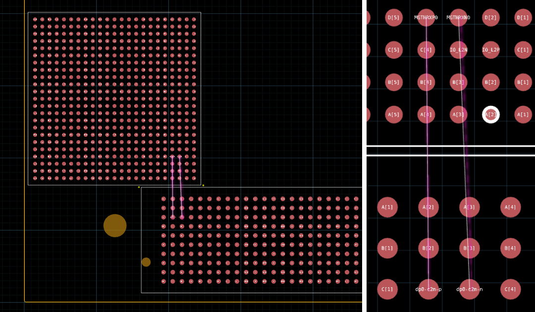
Notice that the differential pair rat's nest only connects to the MGTHRXN0/MGTHRXP0 pair on the FPGA.
#use-added-syntax(jitx)
defpackage fpga_gigabit:
import core
import jitx
import jitx/commands
import ocdb/utils/bundles
import ocdb/utils/box-symbol
public pcb-component VPX-conn :
name = "ASP-134488-01"
description = "Vita 57.1 HPC FMC connector"
manufacturer = "Samtec"
mpn = "ASP-134488-01"
pin-properties :
[pin:Ref | pads:Ref ... | side:Dir | bank:Int]
[dp0-c2m-n | C[3] | Right | 0 ]
[dp0-c2m-p | C[2] | Right | 0 ]
[dp1-c2m-n | A[23] | Right | 0 ]
[dp1-c2m-p | A[22] | Right | 0 ]
pin-properties :
[pin:Ref | clock-capable:(True|False) | gigabit-transceiver:(True|False)]
[dp0-c2m-n | false | true]
[dp0-c2m-p | false | true]
[dp1-c2m-n | false | false]
[dp1-c2m-p | false | false]
make-box-symbol()
assign-landpattern(ASP-134488-01-pkg)
supports diff-pair:
diff-pair.P => self.dp0-c2m-p
diff-pair.N => self.dp0-c2m-n
supports diff-pair:
diff-pair.P => self.dp1-c2m-p
diff-pair.N => self.dp1-c2m-n
public pcb-component Xilinx-FPGA :
name = "Xilinx"
description = "Excerpt of an IO Bank & High Speed Transceiver"
manufacturer = "Xilinx"
pin-properties :
[pin:Ref | pads:Ref ... | side:Dir | bank:Int]
[IO_L2N | C[3] | Right | 0 ]
[IO_L2P | C[2] | Right | 0 ]
[MGTHRXN0 | D[3] | Right | 0 ]
[MGTHRXP0 | D[4] | Right | 0 ]
pin-properties :
[pin:Ref | clock-capable:(True|False) | gigabit-transceiver:(True|False)]
[IO_L2N | false | false]
[IO_L2P | false | false]
[MGTHRXN0 | false | true]
[MGTHRXP0 | false | true]
make-box-symbol()
assign-landpattern(FPGA-pkg)
supports diff-pair:
diff-pair.P => self.IO_L2P
diff-pair.N => self.IO_L2N
supports diff-pair:
diff-pair.P => self.MGTHRXP0
diff-pair.N => self.MGTHRXN0
defn is-gigabit-transceiver (x) -> True|False :
if has-property?(x.gigabit-transceiver):
property(x.gigabit-transceiver)
else:
false
public pcb-module gigabit-restrict-example:
inst fpga : Xilinx-FPGA
inst conn : VPX-conn
require h-dp:diff-pair from fpga
require c-dp:diff-pair from conn
for dp in [h-dp, c-dp] do:
restrict(dp.P, is-gigabit-transceiver)
; Connect the two high-speed capable differential pairs.
net (h-dp, c-dp)
; Land Patterns
defn bga-pkg (pitch:Double, pad-diam:Double, n-pads:[Int Int], courtyard:[Double Double], omit-pads:Tuple<Ref>) :
inside pcb-landpattern :
pcb-pad pin-pad :
type = SMD
shape = Circle(pad-diam / 2.0)
layer(Paste(Top)) = Circle(pad-diam / 2.0)
layer(SolderMask(Top)) = Circle(pad-diam / 2.0)
defn make-pad (r:Int, c:Int) :
val x = ((to-double(n-pads[0]) - 1.0) / -2.0 + to-double(c)) * pitch
val y = ((to-double(n-pads[1]) - 1.0) / 2.0 - to-double(r)) * pitch
; I IS MISSING DELIBERATELY BECAUSE OF SAMTEC's ANNOYING LETTER SCHEME, but O is present.
val letter = ["A" "B" "C" "D" "E" "F" "G" "H" "J" "K" "L" "M" "N" "O" "P" "Q" "R" "S" "T" "U" "V" "W" "X" "Y" "Z"][r]
val name = Ref(letter)[c + 1]
if not contains?(omit-pads, name) :
pad (name) : pin-pad at loc(x, y)
for c in 0 to n-pads[0] do :
for r in 0 to n-pads[1] do :
make-pad(r, c)
layer(Courtyard(Top)) = Rectangle(courtyard[0], courtyard[1])
layer(Silkscreen("pol", Top)) = Circle(-0.3 - courtyard[0] / 2.0, courtyard[1] / 2.0, 0.127)
pcb-landpattern ASP-134488-01-pkg :
bga-pkg(1.27, 0.64, [40 10], [55.78 14.68], [])
; Alignment holes
let:
val xdim = 27.19
val yoff = -3.05
val align-hole-diam = 1.27
; Aligment hole on the right is centered vertically
; Aligment hole on the left is offset vertically
layer(Cutout()) = Circle( xdim, 0.0, align-hole-diam / 2.0)
layer(Cutout()) = Circle( -1.0 * xdim, yoff, align-hole-diam / 2.0)
let:
val xdim = 31.49695
val yoff = 2.006
val standoff-hole-diam = 3.2
; Standoff holes
layer(Cutout()) = Circle( xdim, yoff, standoff-hole-diam / 2.0)
layer(Cutout()) = Circle( -1.0 * xdim, yoff, standoff-hole-diam / 2.0)
pcb-landpattern FPGA-pkg :
bga-pkg(1.0, 0.55, [23, 23], [24.0, 24.0], [])
; Set the design name - a directory with this name will be generated under the "designs" directory
; the board - a Board object
; [optional] rules - the PCB design rules (if not givn default rules will be used)
; [optional] vendors - Strings or AuthorizedVendors (if not give default vendors will be used)
; [optional] quantity - Minimum stock quantity the vendor should carry (if not give default quantity will be used)
public defn setup-design (name:String, board:Board
--
rules:Rules = ocdb/utils/defaults/default-rules
vendors:Tuple<String|AuthorizedVendor> = ocdb/utils/design-vars/APPROVED-DISTRIBUTOR-LIST
quantity:Int = ocdb/utils/design-vars/DESIGN-QUANTITY
bom-columns:Tuple<BOMColumn> = ocdb/utils/design-vars/BOM-COLUMNS) :
set-current-design(name)
set-board(board)
set-rules(rules)
set-bom-vendors(vendors)
set-bom-design-quantity(quantity)
set-bom-columns(bom-columns)
set-paper(ANSI-A4)
set-export-backend(`altium) ; set the CAD software for export to be altium (also supported: `kicad)
val board-shape = RoundedRectangle(100.0, 100.0, 0.25)
setup-design(
"gigabit-restrict-example",
ocdb/utils/defaults/default-board(ocdb/manufacturers/stackups/jlcpcb-jlc2313, board-shape)
)
; Set the schematic sheet size
set-paper(ANSI-A)
; Set the top level module (the module to be compile into a schematic and PCB)
set-main-module(gigabit-restrict-example)
; Use any helper function from helpers.stanza here
; run-check-on-design(my-design)
; View the results
view-board()
view-schematic()
; view-design-explorer()
; view-bom(BOM-STD)
Schematic Group
schematic-group is used to control the organization of our schematic in JITX. The schematic layout engine is allowed to route wires between all of the symbols in a single schematic-group. Wires going between schematic-groups will be broken and have net labels added. The top-level schematic group gets a dotted box drawn around it.
Syntax
pcb-module reg
schematic-group(self) = reg
pcb-module my-module
schematic-group(my-inst) = power
schematic-group(my-other-inst) = test
schematic-group([test-points measure]) = test
schematic-group(load) = schematic-group(my-inst)
; Add one symbol unit from a component with a multi-part symbol
schematic-group(fpga, 0) = power
Description
pcb-module reg :
schematic-group(self) = reg
This statement will apply a schematic group to all of the components that are instantiated inside the module reg. Multiple instances of reg will be grouped individually.
schematic-group(my-inst) = power Set the schematic-group of my-inst to be power.
schematic-group(my-other-inst) = test Set the schematic-group of my-other-inst to be test.
schematic-group([test-points measure]) = test Set the schematic-group of test-points and measure to also be test.
schematic-group(load) = schematic-group(my-inst) Set the schematic-group of load to be the same as the schematic-group of my-inst.
Multi-part Symbol Components
If using a component with a multi-part symbol, the schematic-group statement can be used to add a single sub-part of the symbol to a particular schematic group.
This is often useful when dealing with large, complex components like FPGAs (see A2F200M3F-FGG256I.stanza). For the Microsemi A2F200 FPGA, the pcb-component defines multiple banks, such as the supply, jtag, and analog banks.
inst fpga : ocdb/components/microsemi/A2F200M3F-FGG256I/component
schematic-group(fpga, 0) = power-config ; supply
schematic-group(fpga, 1) = sensors ; analog
schematic-group(fpga, 2) = power-config ; osc
schematic-group(fpga, 3) = power-config ; jtag
In this example, the second argument to schematic-group is the symbol unit index for the bank in question. The symbol unit index is incremented monotonically for every bank.
Short Trace
short-trace gives hints to the placer to keep two pads on different components close together (like a bypass capacitor close to its associated pin). The pads must be on the same net.
Syntax
pcb-module my-module:
net (inst-a.p inst-b.p)
short-trace(inst-a.p inst-b.p)
Description
short-trace(inst-a.p inst-b.p) Keep the p pin of inst-a close to the p pin of 'inst-b' in the layout.
Supports
supports statements can be used in coordination with require statements to automate pin assignment. We use supports to describe valid ways pins can be assigned. A supports statement creates a pending port.
Often supports are used to describe pin mappings on a processor (e.g. a i2c peripheral can map to pins here or here). The support mechanism is very flexible and can make arbitrarily complex mapping constraints.
The supports statement is valid in the following contexts:
Signature
; Single Option Form
supports <TYPE> :
<REQUIRE-1>
...
<TYPE>.<PORT-1> => <ASSIGN-1>
<TYPE>.<PORT-2> => <ASSIGN-2>
...
; Multiple Option Form
supports <TYPE> :
<REQUIRE-1>
...
option:
<REQUIRE-1>
...
<TYPE>.<PORT-1> => <ASSIGN-1>
<TYPE>.<PORT-2> => <ASSIGN-2>
...
option:
<REQUIRE-1>
...
<TYPE>.<PORT-1> => <ASSIGN-3>
<TYPE>.<PORT-2> => <ASSIGN-4>
...
...
<TYPE>- Bundle type that identifies what type of pending port will be constructed<REQUIRE-1>- Optionalrequirestatements that can be used to created nested relationships.<TYPE>.<PORT-1>- Target statement for one of theSinglePinports of<TYPE>.<ASSIGN-1>- A ref to aabstract port, component/module port, or- The
<TYPE>.<PORT-1> => <ASSIGN-1>statements areassignments.
Overview
The supports statement provide a means of constructing a pending port. A pending port on a component or module instance is used to satisfy require statement. A pending port isn't an object or instance like a port, abstract port, or net. It is more ethereal. It provides a means of defining the constraints for making a particular connection as opposed to being a particular port or pin.
Supports Example
pcb-bundle reset:
pin p
pcb-component mcu:
pin-properties:
[pin:Ref | pads:Int ...]
[RESET_n | 5 ]
supports reset:
reset.p => self.RESET_n
In this case, the support reset: statement is constructing a single pending port of type reset. It has one port with only one matching option, self.RESET_n. This support reset: statement acts like an interface definition for the reset signal.
Option Statements
The option statement is a mechanism by which we can define a set of acceptable options for this bundle type. You can think of a supports with option statements as a big element-wise OR gate.
Option Example
pcb-bundle gpio:
pin p
pcb-component mcu:
port PA : pin[16]
supports gpio :
option :
gpio.p => self.PA[1]
option :
gpio.p => self.PA[4]
This supports statement constructs a single pending port of type gpio. This pending port can map to either:
self.PA[1]ORself.PA[4]
In this case, there are only 2 options, but there is no limit. We could add an arbitrary number of option statements.
An Arbitrary Number You Say...
"An arbitrary number seems nice but wouldn't that get rather tedious?" - well yes, but actually no.
This is where typical programming control flow and loop constructs, like for, if, and while, come in. If we take our previous example and expand it from 2 options to 16 options, it might look something like this:
pcb-bundle gpio:
pin p
pcb-compoent mcu:
val num-pins = 16
port PA : pin[ num-pins ]
supports gpio :
for i in 0 to num-pins do:
option:
gpio.p => self.PA[i]
Here - again - we only get 1 gpio pending port from this statement. But now that one gpio can use any of the available IO pins on the PA port of the microcontroller. Progress - now let's open it up a bit more...
Less is More
If we take one more crack at this example and expand our desire from 1 gpio pending port to 16 gpio pending ports with full pin-assignment across the port, we might end up here:
pcb-bundle gpio:
pin p
pcb-component mcu:
val num-pins = 16
port PA : pin[ num-pins ]
for i in 0 to num-pins do:
supports gpio :
gpio.p => self.PA[i]
We don't actually need the option: statement at all to achieve our goal. Just constructing 16 supports gpio: statements is sufficient to create a full cross-bar. Lets consider an example of how this gets used:
inst host : mcu
require switches:gpio[4] from host
This statement basically says, "Give me 4 gpio ports - I don't care which ones right now, we'll decide that later. They just need to be GPIO ports."
This basicaly makes an implicit OR between all of the defined gpio type pending ports that aren't used for some other purpose.
Don't Forget All the Ports
Up to now we've been talking about bundles with a single port, but we can implement supports statements on arbitrarily complex bundles. The key things to remember are:
- Every port of a bundle must have an assignment to form a valid
supportsstatement. - In each
option:statement, every port of a bundle must have an assignment to form a validoptionstatement.
Invalid Support Example
Consider the following as an example that breaks this rule:
pcb-bundle spi:
pin sclk
pin poci
pin pico
pcb-component mcu:
port PB : pin[16]
supports spi:
spi.sclk => self.PB[0]
option:
spi.poci => self.PB[1]
spi.pico => self.PB[2]
option:
spi.poci => self.PB[3]
spi.pico => self.PB[4]
On its face, this looks like a very reasonable structure, but unfortunately it doesn't follow the signatures defined above. The likely goal of this statement is spi.sclk => self.PB[0] for all options. We can implement that logic with explict statements in each option:
Correct Implementation
supports spi:
option:
spi.sclk => self.PB[0]
spi.poci => self.PB[1]
spi.pico => self.PB[2]
option:
spi.sclk => self.PB[0]
spi.poci => self.PB[3]
spi.pico => self.PB[4]
Adding Properties on Assignment
It is often useful to annotate pins that are selected for a particular support function. To support this, properties can be supplied in either the supports statement or the option statements:
pcb-bundle gpio:
pin p
pcb-bundle i2c:
pin sda
pin scl
pcb-component mcu:
val num-pins = 16
port PA : pin[ num-pins ]
for i in 0 to num-pins do:
supports gpio :
gpio.p => self.PA[i]
property(self.PA[i].is-gpio?) = true
supports i2c:
option:
i2c.sda => self.PA[4]
i2c.scl => self.PA[5]
property(self.PA[4].is-i2c?) = true
property(self.PA[5].is-i2c?) = true
option:
i2c.sda => self.PA[11]
i2c.scl => self.PA[12]
property(self.PA[11].is-i2c?) = true
property(self.PA[12].is-i2c?) = true
The property statement at the end of the support/option statement only activates if this support/option is selected by the pin assignment solver. Note that this action does not necessarily happen at compile time. It may happen days or weeks later when a component in the layout moves or a route is completed.
Modules Work Too!
Up to now, we've primarily been referencing components, but don't forget that these techniques apply to pcb-module as well. In fact, modules are where pin assignment can really shine.
Whenever you have multiple components that have a strict constraint between them, use of supports statements in the module can help abstract the details of these complex constraints. They make our code more readable and grok-able.
Let's consider an example where we want to make multiple simple RC filters. Here is a module definition for an RC filter.
This example is intentionally simplfied and does not contain a lot of the detailed engineering you might want in a real circuit, like voltage specs, tolerances, etc. This is primarily for demonstration purposes.
pcb-module low-pass (freq:Double, R-val:Double = 10.0e3) :
port vin : pin
port vout : pin
port gnd : pin
val C-val = 1.0 / ( 2.0 * PI * R-val * freq)
val C-val* = closest-std-val(C-val, 0.2)
inst R : chip-resistor(R-val)
inst C : ceramic-cap(C-val*)
net (vin, R.p[1])
net (R.p[2], C.p[1], vout)
net (C.p[2], gnd)
This filter has a 3-pin interface: vin, vout, and gnd
We want to construct a module that allows us to instantiate some number of these filters, but not necessarily lock ourselves into a specific pin assignment. This is where the supports statements come in at the module level.
We do need to make sure that the input and output pins match though. It would do us no good if the input for channel 1 matched to the output of channel 3. This is where pass-through bundle comes into play:
pcb-bundle pass-through:
port A : pin
port B : pin
pcb-module multi-lpf (ch:Int, freq:Double) :
port gnd : pin
inst lpfs : low-pass(freq)[ch]
for i in 0 to ch do:
net (gnd, lpfs[i].gnd)
for i in 0 to ch do:
supports pass-through:
pass-through.A => lpfs[i].vin
pass-through.B => lpfs[i].vout
The pass-through bundle defines two ports that are matched. These are our vin/vout pair.
Then we construct a pending port of type pass-through for each channel of the multi-lpf definition. With this construction, we get the ability to use the RC filters in any channel location on the board.
Note that the above video just shows the first solution that the Pin Assignment solver was able to deduce. You can route to any valid pin as defined by the require/supports statements of the pin assignment problem.
Here is a link to a complete code example
Nested Require/Support Statements
To make complex constraints, we will often use a cascade of supports statements. We generally call this a Nested require/supports statement. This structure allows us to break down a complex constraint into several simpler constraints and combine them together.
public val UART:Bundle = uart([UART-RX UART-TX UART-RTS UART-CTS])
public pcb-component my-component :
port PA : pin[10]
; Internal (Private) Bundle Definition
pcb-bundle io-pin : (pin p)
for i in 5 to 10 do:
supports io-pin :
io-pin.p => PA[i]
supports UART :
require pins:io-pin[4]
UART.tx => pins[0].p
UART.rx => pins[1].p
UART.rts => pins[2].p
UART.cts => pins[3].p
Our goal is to create a UART pending port that uses any of PA[5], PA[6], PA[7], PA[8], or PA[9] as any of the tx, rx, rts, or cts pins of our UART. This is combinatorics problem.
We accomplish this in two steps:
- Define the set of pins from
PAthat we can select from. - Select from that set to full fill one UART
pending port
We create two kinds of supports statements:
io-pin- This is a private bundle type that only exists withinmy-component.- This defines the set of pins from
PAthat we can select from.
- This defines the set of pins from
UART- Customized UART bundle with our specific pin configuration.- This implements the "Select N from K" using a nested
requirestatement.
- This implements the "Select N from K" using a nested
#use-added-syntax(jitx)
defpackage main :
import core
import math
import jitx
import jitx/commands
import ocdb/utils/generic-components
; Define the shape/size of the board
val board-shape = RoundedRectangle(30.0, 18.5, 0.25)
doc: \<DOC>
RC Low Pass Filter
This is a very crude implementation. This is really
only intended to demonstrate the concept of modules
with multiple components being used as a channel
in pin assignment.
@param freq Corner Frequency for the RC Filter. Must be greater than zero.
@param R-val Resistance value to use by default in the RC filter.
<DOC>
pcb-module low-pass (freq:Double, R-val:Double = 10.0e3) :
port vin : pin
port vout : pin
port gnd : pin
val C-val = 1.0 / ( 2.0 * PI * R-val * freq)
val C-val* = closest-std-val(C-val, 10.0)
inst R : chip-resistor(R-val)
inst C : ceramic-cap(C-val*)
net (vin, R.p[1])
net (R.p[2], C.p[1], vout)
net (C.p[2], gnd)
doc: \<DOC>
Pass Through Connection Bundle
<DOC>
pcb-bundle pass-through:
port A : pin
port B : pin
doc: \<DOC>
Multi-Channel RC Low Pass Filter
@param ch Number of channels to construct
@param freq Cut-off frequency of the filters in Hz. Must be greater than zero.
<DOC>
pcb-module multi-lpf (ch:Int, freq:Double) :
port gnd : pin
inst lpfs : low-pass(freq)[ch]
for i in 0 to ch do:
net (gnd, lpfs[i].gnd)
for i in 0 to ch do:
supports pass-through:
pass-through.A => lpfs[i].vin
pass-through.B => lpfs[i].vout
; Module to run as a design
pcb-module my-design :
net GND
inst J1 : ocdb/components/amphenol/minitek127/component(6)
inst J2 : ocdb/components/amphenol/minitek127/component(6)
net (GND, J1.p[6], J2.p[6])
val chs = 4
inst filters : multi-lpf(chs, 100.0e3)
net (GND, filters.gnd)
require pts:pass-through[chs] from filters
for i in 0 to chs do:
net (J1.p[i + 1], pts[i].A)
net (J2.p[i + 1], pts[i].B)
geom(GND):
copper-pour(LayerIndex(0, Bottom), isolate = 0.2) = board-shape
public defn setup-design (name:String, board:Board
--
rules:Rules = ocdb/utils/defaults/default-rules
vendors:Tuple<String|AuthorizedVendor> = ocdb/utils/design-vars/APPROVED-DISTRIBUTOR-LIST
quantity:Int = ocdb/utils/design-vars/DESIGN-QUANTITY
bom-columns:Tuple<BOMColumn> = ocdb/utils/design-vars/BOM-COLUMNS) :
set-current-design(name)
set-board(board)
set-rules(rules)
set-bom-vendors(vendors)
set-bom-design-quantity(quantity)
set-bom-columns(bom-columns)
set-paper(ANSI-A4)
set-export-backend(`altium) ; set the CAD software for export to be altium (also supported: `kicad)
setup-design(
"jitx-design",
ocdb/utils/defaults/default-board(ocdb/manufacturers/stackups/jlcpcb-jlc2313, board-shape)
)
; Set the schematic sheet size
set-paper(ANSI-A)
; Set the top level module (the module to be compile into a schematic and PCB)
set-main-module(my-design)
; Use any helper function from helpers.stanza here
; run-check-on-design(my-design)
; View the results
view-board()
view-schematic()
view-design-explorer()
view-bom(BOM-STD)
Symbol
symbol(my-net) = my-symbol allows to specify a single-pin symbol my-symbol to attach to a net my-net. This symbol will act as a global label,
that is to say that all nets bearing this symbol will be electrically connected. The main use-case is power symbols.
Syntax
pcb-module my-design :
pin gnd
pin vcc
inst C1 : gen-cap-cmp(0.1e-6)
inst C2 : gen-cap-cmp(0.1e-6)
net gnd (C1.p[1], C2.p[1])
net vcc (C1.p[2], C2.p[2])
symbol(gnd) = ground-sym
symbol(vcc) = supply-sym
Description
Importing the ocdb/utils/symbols package from the open-components-database repository, the ground earth symbol ground-sym and
supply symbol supply-sym can be attached to nets gnd and vcc in this example.
variant
The variant statement provides the flexibility for the design to have variations on the components used. Each variant is identified with its name. The apply-variants command takes a list of variant names and applies them to create the variation specified for the design.
Syntax
pcb-module my-module :
pin power
inst dnp-me : my-component
inst my-res : my-resistor(1000.0)
; Change component status
variant "DNP" :
; Change component status
do-not-populate(dnp-me)
instance-status(dnp-me) :
board-status = NotOnBoard
; Switch the component of an instance
variant "High Reistance" :
component(my-res) = my-resistor(1.0e06)
; Change property "voltage" of a pin
variant "High Power" :
state(power.voltage) = "high"
; Change property "rated-temperature" of the instance my-inst
variant "TOUGH Fuse" :
property(my-inst.rated-temperature) = min-max(-40.0 85.0)
; Apply Variants
val variation = apply-variants(["DNP" "High Power" "High Resistance"] my-module)
set-main-module(variation)
Description
variant "variant name" : Specifies a Variant that may alter the inst in this module.
Its application is determined by a command apply-variants later in top level.
For example, if later on, a top level command
val new-module = apply-variants(["DNP" "High Power"] my-module) is executed, the inst dnp-me will become do-not-populate and power pin will have 5V in new-module.
The following statements are supported within a variant statement:
instance-statusanddo-not-populatestatements modify the on-board and BOM statuses of components.stateandpropertystatements modify the property/state of an instancecomponentstatement replaces the component of an instance by another component, provided they have the same landpattern.
Example Code
#use-added-syntax(jitx)
defpackage my-design :
import core
import jitx
import jitx/commands
import ocdb/utils/defaults
import ocdb/utils/landpatterns
; smd-pad, also needs default rules in ocdb/utils/defaults
pcb-component my-component :
name = "my component"
property(self.rated-temperature) = min-max(-55.0 125.0)
pcb-landpattern my-landpattern :
pad a : smd-pad(Circle(1.0)) at loc(0.0, 0.0) on Top
;pad a : square-pad at loc(0.0, 0.0) on Top
layer(SolderMask(Top)) = Rectangle(1.25, 1.25)
pcb-component my-resistor (resistance:Double):
emodel = Resistor(resistance)
assign-landpattern(my-landpattern)
pcb-module main:
pin gnd
pin power
pin signal
; Change component status
public inst my-inst : my-component
variant "DNP" :
do-not-populate(my-inst)
instance-status(my-inst) :
board-status = NotOnBoard
; Switch the component of an instance to another one with the same landpattern
public inst my-res : my-resistor(10.0e3)
variant "High Resistance":
component(my-res) = my-resistor(10.0e6)
; Change property "voltage" of the pin power
property(power.voltage) = Stateful(["low" => 1.8, "medium" => 3.3, "high" => 5.0])
state(power.voltage) = "low"
variant "High Power" :
state(power.voltage) = "high"
variant "Medium Power" :
state(power.voltage) = "medium"
; Change property "rated-temperature" of the instance fuse
variant "TOUGH Fuse" :
property(my-inst.rated-temperature) = min-max(-40.0 85.0)
; Apply Variants
val variation = apply-variants(["DNP" "High Power" "High Resistance"] main)
set-main-module(variation)
; Verify the variants are properly applied
println $ do-not-populate?(variation.my-inst)
println $ state(variation.power.voltage)
println $ emodel?(variation.my-res)
The output of the above code would be
true
high
Resistor(10000000.0)
Pads
A pcb-pad definition represents a single lead found on a pcb-landpattern.
Syntax
pcb-pad my-pad :
type = SMD ; or TH
shape = Rectangle(1.0, 0.5)
layer(SolderMask(Top)) = Rectangle(1.25, 0.75)
Statements
| Statement | Description |
|---|---|
type | The type of the pad, either SMD (surface mount) or TH (through hole) |
shape | The shape of the pad. |
name | Name |
description | Description |
layer | Layers on the pad, like solder mask and cutouts. |
Name
name is the optional name field of a JITX object. Use it to store a descriptive name as a String. This name will often be used in the UI in place of the object's expression name for better readability.
Signature
name = <String>
Usage
Literal String Names
pcb-component component :
name = "ADM7150"
pcb-module band-pass-filter :
name = "Band-pass filter"
The examples name = "ADM7150" and name = "Band-pass filter" use a String liternal for the name.
Formatted Strings
pcb-pad smd-pad (anchor:Anchor, w:Double, h:Double) :
name = to-string("%_x%_ %_ SMD Pad" % [w,h,anchor])
pcb-landpattern test-lp:
pad p[1] : smd-pad(C, 0.6, 0.7) at loc(x0,y0)
We can also construct strings using formatting routes and parameter arguments for a particular definition. In this example, the constructed smd-pad name property would be 0.6x0.7 C SMD Pad
Description
description is the optional descriptive field of a JITX object. Use it to store a description of the object for human designers reading JITX, and to make the object easier to find via text search. This description also shows up in the UI, such as the design explorer, to provide more insight into particular components and modules in the design.
Signature
description = <String>
Examples
; We can use string literals to describe a particular component.
pcb-component analog-devices-ADM7150 :
description = "800 mA Ultralow Noise, High PSRR, RF Linear Regulator"
; We can use string formatting to construct descriptions based on variables
; or arguments to a JITX Definition
pcb-module band-pass-filter (high-cut:Double, low-cut:Double) :
description = to-string("Band-pass Filter - Highpass = %_ Hz and Lowpass = %_ Hz.")
Layer
The layer statement is used to create geometry on the non-copper layers of a circuit board. The layer() statement is valid in the following contexts:
Signature
layer(<LayerSpecifier>) = <Shape>
<LayerSpecifier>- A LayerSpecifier instance that identifies which non-copper layer to apply the provided geometry to.<Shape>- AShapeinstance that defines the geometry that will be created on the specified layer.
Usage
The most common usage of the layer() statement is in pcb-landpattern:
pcb-landpattern diode-lp :
pad c : smd-pad(0.4, 0.75) at loc(-1.25, 0.0) on Top
pad a : smd-pad(0.4, 0.75) at loc(1.25, 0.0) on Top
layer(Silkscreen("body", Top)) = LineRectangle(1.8, 1.0)
layer(Silkscreen("body", Top)) = Line(0.1, [Point(-0.70, -0.5), Point(-0.70, 0.5)])
layer(Courtyard(Top)) = Rectangle(3.2, 2.0)
layer(ForbidCopper(LayerIndex(0))) = Rectangle(2.0, 1.0)
This will construct a landpattern that looks like this:

Notice the silkscreen in yellow with cathode marker. The blue box is the ForbidCopper layer on the Top Layer. Red is the top copper pads for the cathode c and anode a.
The white bounding rectangle is the Courtyard layer.
See LayerSpecifier for more information about specific layers.
Cutouts
When constructing cutouts in the board layout, your best bet is to use a solid region as opposed to a line. A line can confuse the routing engine into thinking that there are two physically separate regions where copper can be placed.
Consider a USB connector part, U231-096N-3BLRT06-SS, Jing Extension of the Electronic Co.
Here is an excerpt from the datasheet:

If we draw the cutout with a line, as shown in the datasheet, we get this:
pcb-landpattern USB-conn:
...
layer(Cutout()) = Line(0.254, [Point(-7.300, -7.650), Point(-8.450, -7.650)])
layer(Cutout()) = Polyline(0.254, [
Point(6.850, 4.650)
Point(6.850, -7.650)
Point(8.450, -7.650)])
layer(Cutout()) = Polyline(0.254, [
Point(-6.850, 4.650)
Point(-6.850, -7.650)
Point(-7.300, -7.650)])
layer(Cutout()) = Line(0.254, [Point(-6.850, 4.650), Point(6.850, 4.650)])

The cutout line is in gold color. Notice that the ground layer (blue) copper is present on both sides of the cut line with some margin in between. The routing engine basically thinks that the cutout is just the line. If we were making a slot - that would probably be reasonable. But for this case, we want the hole region between the cutout line and the board edge (red) to be a cutout region.
The right way is to use a Rectangle or Polygon solid geometry:
pcb-landpattern USB-conn :
...
layer(Cutout()) = Polygon([
Point(-6.850, 4.650), Point(6.850, 4.650),
Point(6.850, -7.650), Point(-6.850, -7.65),
])
layer(Cutout()) = Circle(Point(-6.85 + 0.5, 4.65), 0.5)
layer(Cutout()) = Circle(Point(6.85 - 0.5, 4.65), 0.5)

Notice that the cutout region fills the entire connector region and the blue ground plane is not present in the cutout region.
Rules
A pcb-rules definition represents the set of design rules associated with a specific circuit board manufacturer.
Syntax
pcb-rules bay-area-circuits-std-rules :
min-copper-width = 0.127
min-copper-copper-space = 0.127
min-copper-hole-space = 0.2032
min-copper-edge-space = 0.381
min-annular-ring = 0.1524
min-drill-diameter = 0.254
min-silkscreen-width = 0.0762
min-pitch-leaded = 0.35
min-pitch-bga = 0.35
max-board-width = 457.2
max-board-height = 609.6
min-silk-solder-mask-space = 0.127
min-silkscreen-text-height = 0.75
solder-mask-registration = 0.106
min-th-pad-expand-outer = 0.2032
min-soldermask-opening = 0.152
min-soldermask-bridge = 0.102
min-hole-to-hole = 0.254
min-pth-pin-solder-clearance = 3.0
Description
All design rules are required to have a value. The supported design rules are :
| Rule Statement | Description |
|---|---|
min-copper-width | Minimum size of a copper feature on a geom. |
min-copper-copper-space | Minimum distance between copper features on the same layer. |
min-copper-hole-space | Minimum distance from a hole or cutout feature to a copper feature on any layer. |
min-copper-edge-space | Minimum distance from the edge of the board to a copper feature on any layer. |
min-annular-ring | Minimum size of the annular ring around a hole or via. |
min-drill-diameter | Minimum diameter of a hole, either in a pad or via. |
min-silkscreen-width | Minimum size of a silkscreen feature. |
min-pitch-leaded | Minimum distance between pad centers of a leaded component. |
min-pitch-bga | Minimum distance between pad centerss of a BGA component. |
max-board-width | Maximum size of a board in the x direction. |
max-board-height | Maximum size of a board in the y direction. |
min-silk-solder-mask-space | Minimum distance between silkscreen and solder mask features. |
min-silkscreen-text-height | Minimum height of text on silkscreen layers. |
min-pth-pin-solder-clearance | Minimum distance between a through hole pad and solder mask. |
solder-mask-registration | Minimum distance from the edge of a copper pad and solder mask feature. |
min-soldermask-opening | Minimum size of a solder mask shape. |
min-soldermask-bridge | Minimum distance between solder mask features. |
min-hole-to-hole | Minimum distance between two holes in pads or vias. |
min-th-pad-expand-outer | Minimum distance from the outer edge of a PTH pad's annular ring to any copper feature. |
Statements
In addition to the set of supported design rules, pcb-rules may have some additional, optional statements.
| Statement | Description |
|---|---|
description | Description |
name | Name |
Name
name is the optional name field of a JITX object. Use it to store a descriptive name as a String. This name will often be used in the UI in place of the object's expression name for better readability.
Signature
name = <String>
Usage
Literal String Names
pcb-component component :
name = "ADM7150"
pcb-module band-pass-filter :
name = "Band-pass filter"
The examples name = "ADM7150" and name = "Band-pass filter" use a String liternal for the name.
Formatted Strings
pcb-pad smd-pad (anchor:Anchor, w:Double, h:Double) :
name = to-string("%_x%_ %_ SMD Pad" % [w,h,anchor])
pcb-landpattern test-lp:
pad p[1] : smd-pad(C, 0.6, 0.7) at loc(x0,y0)
We can also construct strings using formatting routes and parameter arguments for a particular definition. In this example, the constructed smd-pad name property would be 0.6x0.7 C SMD Pad
Description
description is the optional descriptive field of a JITX object. Use it to store a description of the object for human designers reading JITX, and to make the object easier to find via text search. This description also shows up in the UI, such as the design explorer, to provide more insight into particular components and modules in the design.
Signature
description = <String>
Examples
; We can use string literals to describe a particular component.
pcb-component analog-devices-ADM7150 :
description = "800 mA Ultralow Noise, High PSRR, RF Linear Regulator"
; We can use string formatting to construct descriptions based on variables
; or arguments to a JITX Definition
pcb-module band-pass-filter (high-cut:Double, low-cut:Double) :
description = to-string("Band-pass Filter - Highpass = %_ Hz and Lowpass = %_ Hz.")
Routing Structures
Routing structures are definitions that specify geometric constraints on nets and topologies.
| Statement | Description |
|---|---|
pcb-routing-structure | Routing Structures for Single-Ended Topologies |
pcb-differential-routing-structure | Routing Structures for Differential Topologies |
pcb-routing-structure
The pcb-routing-structure is a statement for defining the geometric constraints of a single-ended topology. This may include:
- Singled-ended transmission lines, like microstrip and striplines.
- Uncoupled regions for differential pair transmission lines.
- Fanout regions for BGAs or other dense components.
Outline
pcb-routing-structure struct-name (arg1:Type1, ...) :
name = <String>
description = <String>
layer(<LayerIndex|Side>):
trace-width = <Double> ; mm
clearance = <Double> ; mm
velocity = <Double> ; mm/s
insertion-loss = <Double> ; dB/mm
; Option #1 - NeckDown Instance
neck-down = <Neckdown>
; Option #2 - NeckDown Macro
; Notice the `:` instead of `=`
neck-down :
trace-width = <Double>
clearance = <Double> ; mm
velocity = <Double> ; mm/s
insertion-loss = <Double> ; dB/mm
layer(<LayerIndex|Side>):
...
The routing structure requires an expression name struct-name that uniquely identifies this statement within the current context.
The arguments list (arg1:Type1, ...) is optional and provides a means to parameterize routing structures for common statements.
The name and description properties are optional and are primarily for documentation and labeling purposes. The name property in particular is typically for UI applications. If a name property is not provided, then the expression name struct-name will be used.
The elements of the pcb-routing-structure statement are identified using a layer statement. Each of these layer statements must match with a conductor layer in the pcb-stackup defined for the current board design. Conceptually, the idea is to apply different properties depending on the layer.
The layer() statement takes an argument of either a Side like Top or Bottom, or a LayerIndex. See LayerIndex for more information.
At each layer specification, the user can list any of these properties:
- Required Properties:
trace-width- Width in mm of the traces on this layer.velocity- Signal Propagation Velocity (also known as Group Velocity) of the signals on this layer. This is primarily used for timing constraints. This property is in unitsmm/s.insertion-loss- Insertion Loss per unit distance of the signals on this layer. This property is in units ofdB/mm
- Optional Properties
clearance- Minimum "Net to Net" clearance in mm of the traces on this layer. If not provided, then the default minimum clearances from the design rules will be used.neckdown- This property allows the user to specify a special set of routing properties for the neck down region. It comes in two forms:- Instance Form - the user must assign a NeckDown instance.
- Macro Form - the user can provide, directly, statements for
trace-width,clearance, etc like above.
If these properties are not explicitly provided in the routing structure, then either:
- The default design rules for the board will be consulted for
trace-widthandclearance - If there are timing or loss constraints on this route, but no defined structure information for layers that have traces, then default values will be used for
velocityandinsertion-loss. The current default values are:velocity = 0.15e12 ; mm/sinsertion-loss = 0.002 ; dB/mm
Usage
Here are a list of common examples:
Microstrip Example
val eps-r = 4.6
val vel = phase-velocity(eps-r)
val target-imped = 50.0
val thickness = 0.035 ; mm
val height = 0.1; mm
; Compute an estimate of the trace width
; for a 50 ohm impedance.
val w = ipc2141-microstrip-width(
target-imped, eps-r, thickness, height
)
public pcb-routing-structure se-50 :
name = "50 Ohm Microstrip"
layer(Top) :
trace-width = w
clearance = w * 3.0
velocity = vel
insertion-loss = 0.008
layer(Bottom) :
trace-width = w
clearance = w * 3.0
velocity = vel
insertion-loss = 0.008
In this example, we construct a microstrip transmission line for the Top and Bottom layers.
Caution!
This routing structures does not provide parameters for any of the internal layers. If any of the routes that have this routing structure assigned to them transition to an internal layer, then the runtime will consult the default design rules for the trace width constraint.
Using Generator Functions
Some times, we would like to construct repeated definitions in the internal layers of a board. We can use a generator function to construct these internal layers without copy/pasting code.
; Generator for constructing a stripline at 75 ohm
; on a target internal layer.
defn gen-internal-stripline (l:LayerIndex) :
val w = 0.12
inside pcb-routing-structure:
layer(l):
trace-width = w
clearance = 3.0 * w
velocity = 0.19e12 ; mm / s
insertion-loss = 0.008 ; dB / mm
pcb-routing-structure se-75:
name = "75 ohm Single-Ended"
val ms-w = 0.095
layer(Top):
trace-width = ms-w
clearance = 3.0 * ms-w
velocity = 0.19e12
insertion-loss = 0.008
for sig-layer in [2, 5, 7] do:
gen-internal-stripline(LayerIndex(sig-layer))
layer(Bottom):
trace-width = ms-w
clearance = 3.0 * ms-w
velocity = 0.19e12
insertion-loss = 0.008
In this example, we use a generator function to construct the layer() statement for the internal layers. We then use a for-loop to construct that same structure multiple times.
The resulting pcb-routing-structure object has the following layer statements:
layer(Top)withtrace-width = 0.095layer(LayerIndex(2))withtrace-width = 0.12layer(LayerIndex(5))withtrace-width = 0.12layer(LayerIndex(7))withtrace-width = 0.12layer(Bottom)withtrace-width = 0.095
Using NeckDown
; Define a single-ending routing structure for the
; uncoupled regions
public pcb-routing-structure se-100 ( -- clearance-mult:Double = 3.0 ) :
name = "100 Ohm Microstrip"
val w-100 = 0.1048
layer(Top) :
trace-width = w-100
clearance = w-100 * clearance-mult
velocity = 0.19e12
insertion-loss = 0.008
neckdown = NeckDown(
clearance = 0.5 * clearance-mult * w-100
)
...
; Application
structure(A => B) = se-100( clearance-mult = 2.5 )
Here the neckdown property is used to change the clearance properties of neckdown traces on the Top layer.
pcb-differential-routing-structure
The pcb-differential-routing-structure is a statement for defining the geometric constraints of a differential pair topology. This definition applies to only the coupled region of a differential pair.
Outline
pcb-differential-routing-structure struct-name (arg1:Type1, ...) :
name = <String>
description = <String>
uncoupled-region = <RoutingStructure>
layer(<LayerIndex|Side>):
trace-width = <Double> ; mm
pair-spacing = <Double> ; mm
clearance = <Double> ; mm
velocity = <Double> ; mm/s
insertion-loss = <Double> ; dB/mm
; Option #1 - DifferentialNeckDown Instance
neck-down = <DifferentialNeckDown>
; Option #2 - Macro Form
; Notice the `:` instead of `=`
neck-down:
trace-width = <Double>
pair-spacing = <Double> ; mm
clearance = <Double> ; mm
velocity = <Double> ; mm/s
insertion-loss = <Double> ; dB/mm
layer(<LayerIndex|Side>):
...
The routing structure requires an expression name struct-name that uniquely identifies this statement within the current context.
The arguments list (arg1:Type1, ...) is optional and provides a means to parameterize routing structures for common statements.
The name and description properties are optional and are primarily for documentation and labeling purposes. The name property in particular is typically for UI applications. If a name property is not provided, then the expression name struct-name will be used.
The uncoupled-region property is used to apply a particular single-ended routing structure (ie, a pcb-routing-structure) to the uncoupled regions of a differential pair. This typically applies to via breakouts, fanout from an IC, etc.
The elements of the pcb-differential-routing-structure statement are identified using a layer statement. Each of these layer statements must match with a conductor layer in the pcb-stackup defined for the current board design. Conceptually, the idea is to apply different properties depending on the layer.
The layer() statement takes an argument of either a Side like Top or Bottom, or a LayerIndex. See LayerIndex for more information.
At each layer specification, the user can list any of these properties:
- Required Properties:
trace-width- Width in mm of both of the diff-pair conductors for any traces on this layer.pair-spacing- Spacing distance between the conductors of the differential pair in mm.velocity- Signal Propagation Velocity (also known as Group Velocity) of the signals on this layer. This is primarily used for timing constraints. This property is in unitsmm/s.insertion-loss- Insertion Loss per unit distance of the signals on this layer. This property is in units ofdB/mm
- Optional Properties
clearance- Minimum "Net to Net" clearance in mm of the traces on this layer. If not provided, then the default minimum clearances from the design rules will be used. This clearance does not affect thepair-spacingfor the differential pair.neckdown- This property allows the user to specify a special set of routing properties for the neck down region. It comes in two forms:- Instance Form - the user must assign a DifferentialNeckDown instance.
- Macro Form - the user can provide, directly, statements for
trace-width,pair-spacing,clearance, etc like above.
If these properties are not explicitly provided in the routing structure, then either:
- The default design rules for the board will be consulted for
trace-widthandclearance - If there are timing or loss constraints on this route, but no defined structure information for layers that have traces, then default values will be used for
velocityandinsertion-loss. The current default values are:velocity = 0.15e12 ; mm/sinsertion-loss = 0.002 ; dB/mm
Usage
Below are some typical examples of differential routing structures in action.
Edge Coupled Microstrip
; Define a single-ending routing structure for the
; uncoupled regions
public pcb-routing-structure se-100 ( w:Double = 0.1048 ) :
name = "100 Ohm Microstrip"
layer(Top) :
trace-width = w
clearance = w * 3.0
velocity = 0.19e12
insertion-loss = 0.008
layer(Bottom) :
trace-width = w
clearance = w * 3.0
velocity = 0.19e12
insertion-loss = 0.008
val ec-stripline-ph-vel = 0.19e12 ; mm / s @ 1GHz
val ec-stripline-loss = 0.008 ; dB/mm @ 1GHz
public pcb-differential-routing-structure diff-100 :
name = "100 Ohm differential impedance"
uncoupled-region = se-100()
layer(Top) :
trace-width = 0.0762 ; mm - 3mil
pair-spacing = 0.127 ; mm - 5mil
clearance = 0.3 ; mm
velocity = ec-stripline-ph-vel ; mm/s
insertion-loss = ec-stripline-loss ; dB/mm @ 1GHz
layer(Bottom) :
trace-width = 0.0762 ; mm - 3mil
pair-spacing = 0.127 ; mm - 5mil
clearance = 0.3 ; mm
velocity = ec-stripline-ph-vel ; mm/s
insertion-loss = ec-stripline-loss ; dB/mm @ 1GHz
In this example, we define two routing structures - a singled ended 100 ohm version and a differential 100 ohm impedance version. The single-ended routing structure is used for the uncoupled regions of the differential pair due to the uncoupled-region statement.
NeckDown
There are two types for describing the neck down region of a trace:
NeckDown- This targets Single-Ended tracesDifferentialNeckDown- This targets Differential Pair traces
Outline - NeckDown
defstruct NeckDown :
trace-width: Double|False
clearance: Double|False
insertion-loss: Double|False
velocity: Double|False
defn NeckDown (-- trace-width: Double|False = false,
clearance: Double|False = false,
insertion-loss: Double|False = false,
velocity: Double|False = false) -> NeckDown :
...
All properties of the NeckDown object are optional. If a property is
not provided in the instance, then the pcb-routing-structure property for the current layer will be used by default. These properties act as overrides of the routing structure properties in the neckdown region of a trace.
trace-width- Width of the trace in mmclearance- Minimum "Net to Net" clearance in mm of the tracesvelocity- Signal Propagation Velocity (also known as Group Velocity) of the signals in the neckdown region. This is primarily used for timing constraints. This property is in unitsmm/s.insertion-loss- Insertion Loss per unit distance of the signals in the neckdown region. This property is in units ofdB/mm
Usage - NeckDown
pcb-routing-structure se-50 :
layer(Top):
trace-width = 0.12
clearance = 0.2
velocity = 0.19e12
insertion-loss = 0.008
neckdown = NeckDown(
width = 0.085
clearance = 0.15
insertion-loss = 0.012
)
In this example - the neckdown region overrides the width, clearance, and insertion-loss but leaves the velocity property with the default 0.19e12 value.
Outline - DifferentialNeckDown
defstruct DifferentialNeckDown :
pair-spacing: Double|False
trace-width: Double|False
clearance: Double|False
insertion-loss: Double|False
velocity: Double|False
defn DifferentialNeckDown (-- pair-spacing: Double|False = false,
trace-width: Double|False = false,
clearance: Double|False = false,
insertion-loss: Double|False = false,
velocity: Double|False = false) -> DifferentialNeckDown :
All properties of the DifferentialNeckDown object are optional. If a property is
not provided in the instance, then the pcb-differential-routing-structure property for the current layer will be used by default. These properties act as overrides of the routing structure properties in the neckdown region of a differential trace.
trace-width- Width in mm of both of the diff-pair conductors.pair-spacing- Spacing distance between the conductors of the differential pair in mm.clearance- Minimum "Net to Net" clearance in mm of the traces. This clearance does not affect thepair-spacingfor the differential pair.velocity- Signal Propagation Velocity (also known as Group Velocity) of the signals in the neckdown region. This is primarily used for timing constraints. This property is in unitsmm/s.insertion-loss- Insertion Loss per unit distance of the signals in the neckdown region. This property is in units ofdB/mm
Usage - DifferentialNeckDown
pcb-differential-routing-structure diff-85 :
layer(Top):
trace-width = 0.12
pair-spacing = 0.127
clearance = 0.3
velocity = 0.19e12
insertion-loss = 0.008
neckdown = DifferentialNeckDown(
clearance = 0.15
)
In this example - the neckdown region overrides the clearance but leaves all other properties untouched.
pcb-stackup
The pcb-stackup statement is used to define the physical layer stack for the PCB. This includes the copper, dielectric, and soldermask layers. The definitions inside the pcb-stackup statement are used to inform the JITX runtime about the available copper layers and other features.
Signature
pcb-stackup stackup-name (arg1:Type1, ...) :
name = <String|False>
description = <String|False>
<LAYER-1>
...
The expression name stackup-name uniquely identifies this stackup definition
in the current context.
The argument list (arg1:Type1, ...) is optional and provides a means of
constructing parameterized stackup definitions.
- Required Parameters
<LAYER-1>- The stackup is composed of multiple layer() statements which define the construction of the stackup. Each layer can be a different material.
- Optional Parameters
name- This name is used in the UI as a more user friendly name. If this string is not provided then thestackup-nameexpression is used as the stackup's name.description- This string is defining more meta-data for the stackup - such as the fabricator or manufacturer of this stackup.
Usage
A typical stackup will consist of multiple copper layers separated by resin core and prepreg layers. Here is an example of a 8-layer construction typical of controlled impedance applications:
pcb-material soldermask :
type = Dielectric
dielectric-coefficient = 3.2
loss-tangent = 0.012
pcb-material copper:
type = Conductor
pcb-material prepreg-2x2113:
type = Dielectric
dielectric-coefficient = 4.2
loss-tangent = 0.02
pcb-stackup std-stackup :
name = "8-layer 1.6mm"
val cu-1oz = 0.035
val H = 0.1524
layer(0.019, soldermask)
layer(cu-1oz, copper)
layer(H, prepreg-2x2113)
layer(cu-1oz, copper, "GND1")
layer(H, prepreg-2x2113)
layer(cu-1oz, copper, "SIG1")
layer(H, prepreg-2x2113)
layer(cu-1oz, copper, "GND2")
layer(H, prepreg-2x2113)
layer(cu-1oz, copper, "PWR1")
layer(H, prepreg-2x2113)
layer(cu-1oz, copper, "GND3")
layer(H, prepreg-2x2113)
layer(cu-1oz, copper, "SIG2")
layer(H, prepreg-2x2113)
layer(cu-1oz, copper)
layer(0.019, soldermask)
In this example, all of the layers are separated by a 2x2113 ply prepreg dielectric. The copper layers are all 1oz/ft^2 (35um) thickness.
The strings on the inner copper layers provides overriding names for the copper layers. These names will be used in the layer visualizer to provide an easier mnemonic.
Complex Prepreg Ply Structure
In order to achieve the desired dielectric thickness required for some applications, we need to combine different ply constructions together. We can do this by defining separate materials for each prepreg.
Here is a 4-layer construction where the prepreg layer is a combination of a 1x2113 and 1x2116:
pcb-material core-FR4 :
type = Dielectric
dielectric-coefficient = 4.5
loss-tangent = 0.008
pcb-material soldermask :
type = Dielectric
dielectric-coefficient = 3.2
loss-tangent = 0.012
pcb-material copper:
type = Conductor
pcb-material prepreg-FR4-2113:
type = Dielectric
dielectric-coefficient = 4.5
loss-tangent = 0.008
pcb-material prepreg-FR4-2116:
type = Dielectric
dielectric-coefficient = 4.5
loss-tangent = 0.008
pcb-stackup prepreg-stackup :
name = "4-layer 1.6mm"
layer(0.019, soldermask)
layer(0.035, copper)
layer(0.0762, prepreg-FR4-2113)
layer(0.1067, prepreg-FR4-2116)
layer(0.035, copper)
layer(1.0, core-FR4)
layer(0.035, copper)
layer(0.1067, prepreg-FR4-2116)
layer(0.0762, prepreg-FR4-2113)
layer(0.035, copper)
layer(0.019, soldermask)
Constructs the following stackup:
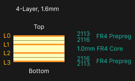
Notice that the 2113 and 2116 ply prepreg layers are adjacent to each other. This will allow us to construct an accurate PCB stackup table in the drawings.
Checks on Invalid Stackups
One limitation of the pcb-stackup is that Conductor type material layers must be separated by a Dielectric layer.
For example, if we construct a pcb-stackup with two adjacent copper layers:
pcb-stackup invalid-stackup :
name = "2-layer 1.6mm"
layer(0.019, soldermask)
layer(0.035, copper)
; Invalid Copper Layer Here!
layer(0.035, copper)
layer(1.0, core-FR4)
layer(0.035, copper)
layer(0.019, soldermask)
This will throw the following exception when we use this stackup in the board for the current design:
Uncaught Exception: Stackups cannot have two adjacent conductor layers.
Using Generators
Generators are method of composition. In the pcb-stackup, we can use a generator to help reduce duplication in our stackup generation.
Note - This is a more complex example. Fear not! These structures will make sense as you gain more experience in the JITX environment.
This example builds on the pcb-material definitions from the 8-layer example stackup above:
defn add-layer (
H:Double, cu:Double,
--
di-mat:Material = prepreg-FR4-2x2113,
cu-mat:Material = copper
cu-name:String = ?
):
inside pcb-stackup:
layer(H, di-mat)
match(cu-name):
(cu-n:One<String>):
layer(cu, cu-mat, value(cu-n))
(_:None):
layer(cu, cu-mat)
pcb-stackup prepreg-stackup :
name = "8-layer 1.6mm"
val cu-1oz = 0.035
val H = 0.1524
layer(0.019, soldermask)
layer(cu-1oz, copper)
add-layer(H, cu-1oz, cu-name = "GND1")
add-layer(H, cu-1oz, cu-name = "SIG1")
add-layer(H, cu-1oz, cu-name = "GND2")
add-layer(H, cu-1oz, cu-name = "PWR1")
add-layer(H, cu-1oz, cu-name = "GND3")
add-layer(H, cu-1oz, cu-name = "SIG2")
add-layer(H, cu-1oz)
layer(0.019, soldermask)
The inside pcb-stackup expression converts the function add-layer into a generator. When this function is called from a pcb-stackup context, it can generate statements into statements like layer() into the parent pcb-stackup context. If you were to call this function from a different context (eg, from a pcb-module), then this function would throw an error because the layer() statement would be unknown in that context.
In this case, the add-layer generator injects a dielectric layer and a copper layer with thicknesses based on the H and cu arguments, respectively. It uses default arguments for the dielectric and conductor materials to reduce the number of arguments we must pass.
The cu-name:String = ? is a special kind of default argument. You can think of cu-name not as a pure String but as a Maybe<String> - see stanza's reference on Maybe for more info. This drives the need for the match statement on the cu-name argument to differentiate between None and One<String>.
The constructed pcb-stackup object from this excerpt should match the 8-Layer stackup defined here.
Statements
| Statement | Description |
|---|---|
layer | Define a layer in the stackup |
Stackup Layers
The layer statement inside a pcb-stackup declares a physical copper or dielectric layer within the stackup.
Signature
layer(<HEIGHT>, <MATERIAL>)
layer(<HEIGHT>, <MATERIAL>, <NAME>)
<HEIGHT>- This is an instance of typeDoublethat indicates the layer's vertical (Z-axis) height in mm<MATERIAL>- This is a pcb-material object that defines the physical material for this layer.<NAME>- This is an instance of typeStringthat indicates the name of this layer.- For copper layers, this string will be used in the layer visualizer of the board view.
- If no
<NAME>string is provided then a default set of names will be used:TopandBottomfor their respective copper layers- For inner layers, we use
Inner 1,Inner 2, etc.
Usage
The pcb-stackup statement utilizes these layer() statements to construct the physical board stackup. The ordering of the layer() statements is important and defines the physical layer order.
pcb-material copper:
type = Conductor
pcb-material soldermask:
type = Dielectric
pcb-material core-45:
type = Dielectric
pcb-stackup simple-2-layer :
layer(0.019, soldermask) ; 0.5mil over conductor
layer(0.035, copper)
layer(1.5, core-45)
layer(0.035, copper)
layer(0.019, soldermask) ; 0.5mil over conductor
pcb-via
The pcb-via statement is used to define a type of via that can instantiated
in the board view. All via types are defined in code. This allows you to:
- Create a known set of vias with particular characteristics
- Create a known rule set for these vias to avoid deviations.
- Maintain this via set and edit all vias of a particular type in one place.
- Reuse existing via definition sets from project to project.
Outline
pcb-via via-name (arg1:Type1, ...) :
name = <String>
description = <String>
start = <LayerIndex|Side>
stop = <LayerIndex|Side>
diameter = <Double>
hole-diameter = <Double>
type = <MechanicalDrill|LaserDrill>
filled = <True|False>
tented = <Side|Both|True|False>
via-in-pad = <True|False>
backdrill = <BackDrill|False>
The expression name via-name uniquely identifies this via definition
in the current context.
The argument list (arg1:Type1, ...) is optional and provides a means of
constructing parameterized via definitions.
- Required Parameters
start- Sets the starting layer for the via. Setting this to something other than the top layer allows for creating buried or blind vias.stop- Sets the ending layer for the via.diameter- Pad diameter in mm for the viahole-diameter- Drilled or Lasered hole diameter in mm for the via.type- Identifies the type of via, either mechanical drill or laser microvia.
- Optional Parameters
name- This name is used in the Board UI as a more user friendly name. If this string is not provided then thevia-nameexpression is used as the via's name.description- This string is defining more meta-data for the via.filled- Indicates whether this via is filled or not.tented- Specifies whether or not there is a soldermask opening for this via on top, bottom, or both sides.via-in-pad- Specifies whether this via is allowed to be placed inside a component's pads.backdrill- Specifies whether or not this via is backdrilled See BackDrill
Usage
Here are a list of common examples:
Default Through-Hole
Here is a minimal example pcb-via statement:
pcb-via default-th:
name = "Std TH"
start = Top
stop = Bottom
diameter = 0.6 ; mm
hole-diameter = 0.3 ; mm
type = MechanicalDrill
This constructs what would be consided a typical through-hole via that traverses the board stackup from Top to Bottom layers.
Microvia - Top & Bottom
Here is a minimal example for a microvia on the top side of the board from the top layer to the first inner layer from the top:
public pcb-via top-uvia :
name = "Top-0-1-uvia"
start = LayerIndex(0, Top)
stop = LayerIndex(1, Top)
diameter = 0.15
hole-diameter = 0.1
type = LaserDrill
tented = Top
Another Example but on the bottom side:
public pcb-via bot-uvia :
name = "Bot-0-1-uvia"
start = LayerIndex(1, Bottom)
stop = LayerIndex(0, Bottom)
diameter = 0.15
hole-diameter = 0.1
type = LaserDrill
tented = Bottom
Notice that the LayerIndex when starting from the bottom of the board has
the layer indices in the reverse order.
pcb-via with Arguments
Here is an example of constructing a pcb-via with arguments.
public pcb-via buried (st:Int, end:Int) :
name = to-string("Buried-%_-%_" % [st, end])
start = LayerIndex(st, Top)
stop = LayerIndex(end, Top)
diameter = 0.35
hole-diameter = 0.2
type = MechanicalDrill
Notice that I've used the name property so that different
invokations of buried will construct uniquely named vias.
This via can then be used in the pcb-board definition like this:
public pcb-board mem-board :
stackup = mem-stackup
boundary = board-shape
signal-boundary = board-shape
vias = [default-th-via, top-uvia, bot-uvia, buried(1, 10)]
Notice that we pass the start and end layer for the buried via.
Watch Out!
There are a few things to look out for when defining vias:
- Renaming a via definition in code can cause any instantiated vias in the board design to become invalid.
- Invalid means that the via gets labeled with a red X
- This only applies to vias that have been placed in the board view. If no vias of this type exist in the board yet, then this definition can be renamed at will.
- Examples for changing a via name:
- If there is no
nameproperty and you change the via's expression name (ie changetop-uviatomy-uviafrom the above example) - If there is no
nameproperty and you add anameproperty with a value that is different from the expression name. - If there is an existing
nameproperty and you changed that string. - If the name is defined via arguments to the definition and the arguments change.
- If there is no
Backdrill Type
The Backdrill type is used to define the parameters for a backdrilled via.
val bd = Backdrill(
Bottom, ; Side - Top / Bottom
LayerIndex(4, Bottom), ; Stop Layer
0.4 ; drill diameter, mm
0.6 ; starting pad diameter, mm
0.8 ; Soldermask Opening diameter, mm
1.0 ; Copper Clearance Diameter, mm
)
The Backdrill can be defined from either the bottom side or the top side.
The second parameter defined the stop layer, which is the copper layer that
is the drill boundary.
In this example - the drill depth is computed from the sum of the copper and dielectric layers from the Bottom layer to 5 copper layer (zero-indexed value) from the bottom. The 5th copper layer from the bottom is the layer that will conduct signal for this via. The 1-4th copper layers from the bottom will be drilled out and not able to conduct or form a stub.
Schematic Symbol Statements
The pcb-symbol statement defines an object that encodes the schematic representation of a part. This definition includes:
- The electrical connection points for the symbol (ie, the pins).
- The geometric artwork for the symbol.
- Text annotations such as part number, designator, etc.
Each pcb-symbol defines an internal coordinate frame. All of the geometry, pins, and other features of the symbol are defined with respect to that internal coordinate frame.
The JITX OCDB has a large collection of predefined symbols you can use directly or as templates. The make-box-symbol() function is a powerful tool to quickly create a consistent looking part library.
For more information about how pcb-symbol definitions are used, see the symbol statement as it applies to the pcb-component definition.
Signature
pcb-symbol symbol-name (arg1:Type1, ...) :
name = <String|False>
description = <String|False>
preferred-orientation = <SymbolOrientation|False>
backend-substitution(<String>) = <SchematicSymbol>
<PIN-1>
...
<LAYER-1>
...
The expression name symbol-name uniquely identifies this symbol definition
in the current context.
The argument list (arg1:Type1, ...) is optional and provides a means of
constructing parameterized symbol definitions.
- Parameters
name- This name is used in the UI as a more human readable name. If this string is not provided, then thesymbol-nameexpression is used as the symbol's name.description- This string provides documentation and further context when needed.- preferred-orientation - Marks the preferred rotational orientation of this symbol. Default is no preference for any particular orientation.
- backend-substitution - Tool for swapping a schematic symbol depending on which export backend is being used.
<PIN-1>- A pin statement which defines a connection point to the symbol in the symbol's coordinate frame.<LAYER-1>- A layer statement which provides a means of inserting symbol artwork into the symbol's coordinate frame.
Non-Box Symbol Example
For more unusual components where box symbols may not apply, you can draw symbols the same way you can draw any collections of shapes in JITX. On imported components, the symbols may appear as collections of lines, shapes, and text.
; Wurth 760390015
pcb-symbol sym-760390015 :
val L = 5.08
val font-size = 1.0
pin p[1] at Point(-5.080, 7.620) with :
direction = Left
length = L
name-size = font-size
pin p[2] at Point(-5.080, 0.0) with :
direction = Left
length = L
name-size = font-size
pin p[3] at Point(-5.080, -7.620) with :
direction = Left
length = L
name-size = font-size
pin p[4] at Point(5.080, -7.620) with :
direction = Right
length = L
name-size = font-size
pin p[5] at Point(5.080, 0.0) with :
direction = Right
length = L
name-size = font-size
pin p[6] at Point(5.080, 7.620) with :
direction = Right
length = L
name-size = font-size
layer("value") = Text(">VALUE", 0.7056, C, loc(0.0, 8.620))
layer("reference") = Text(">REF", 0.7056, C, loc(0.0, 9.620))
layer("foreground") = Circle(-2.794, 6.858, 0.254)
layer("foreground") = Circle(2.540, 6.858, 0.254)
layer("foreground") = Circle(2.540, -0.762, 0.254)
layer("foreground") = Circle(-2.540, -0.762, 0.254)
layer("foreground") = Polyline(0.254, [
Point(-5.080, 7.620)
Point(-2.540, 7.620)])
layer("foreground") = Polyline(0.254, [
Point(-0.6, -7.620)
Point(-0.6, 7.620)])
layer("foreground") = Polyline(0.254, [
Point(0.6, -7.620)
Point(0.6, 7.620)])
layer("foreground") = Polyline(0.254, [
Point(5.080, -7.620)
Point(2.540, -7.620)])
; Coils
layer("foreground") = Polyline(0.254, [
Point(-5.080, 0.0) ; Center Tap
Point(-2.540, 0.0)
Arc(-2.540, 1.270, 1.270, 270.000, 180.0)
Arc(-2.540, 3.810, 1.270, 270.000, 180.0)
Arc(-2.540, 6.350, 1.270, 270.000, 180.0)
Point(-2.540, 7.620)
Point(-5.080, 7.620)
])
layer("foreground") = Polyline(0.254, [
Point(5.080, 7.620)
Point(2.540, 7.620)
Arc(2.540, 6.350, 1.270, 90.000, 180.000)
Arc(2.540, 3.810, 1.270, 90.000, 180.000)
Arc(2.540, 1.270, 1.270, 90.000, 180.000)
Point(2.540, 0.0) ; Center Tap
Point(5.080, 0.0)
])
layer("foreground") = Polyline(0.254, [
Arc(2.540, -1.270, 1.270, 90.000, 180.000)
Arc(2.540, -3.810, 1.270, 90.000, 180.000)
Arc(2.540, -6.350, 1.270, 90.000, 180.000)
Point(2.540, -7.620)
Point(5.080, -7.620)
])
layer("foreground") = Polyline(0.254, [
Point(-5.080, -7.620)
Point(-2.540, -7.620)
Arc(-2.540, -6.350, 1.270, 270.000, 180.000)
Arc(-2.540, -3.810, 1.270, 270.000, 180.000)
Arc(-2.540, -1.270, 1.270, 270.000, 180.000)
])
This generates a symbol that looks like this:
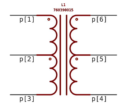
Statements
Here is the list of all of the statements you can use in a pcb-symbol :
| Statement | Description |
|---|---|
backend-substitution | Backend Substition |
description | Description |
layer | Layer |
name | Name |
pin | Pin |
preferred-orientation | Preferred Orientation |
backend-substitution
The backend-substituion statement is used to customize the symbol generation when exported to a particular backend, like Kicad or Altium.
This
backend-substitution statement is primarily useful for net symbols like the ground
symbol or the power arrow symbol. Certain backends have a restricted set of net symbols that can be created in these cases. This statement allows the user to customize which
symbol will be used on these backends.
Altium ground and supply symbols are in the ocdb/utils/symbols package of the open-components-database repository.
Signature
backend-substitution(<String>) = <SchematicSymbol>
...
<String>- A string literal for the backend this statement targets.- "Altium" targets "Altium Designer" export
- "Kicad" targets "Kicad" export.
<SchematicSymbol>- A schematic symbol definition created using thepcb-symbolstatement.
Usage
For certain symbols, we might want to customize the symbol construction depending on the backend (ie, the export target).
public pcb-symbol ground-sym :
pin p[0] at unit-point(0.0, 0.0)
unit-line([[0.0, 0.0], [0.0, -0.5]])
unit-line(0.1, [[-0.5, -0.5], [0.5, -0.5]])
unit-line(0.1, [[-0.3, -0.7], [0.3, -0.7]])
unit-line(0.1, [[-0.1, -0.9], [0.1, -0.9]])
unit-val([-1.0, -1.5])
preferred-orientation = PreferRotation([0])
backend-substitution("Altium") = altium-power-gnd-power-sym
Here the default symbol geometry gets created on all platforms except Altium, which gets a customized Power Port Symbol, specifically, the "Power Ground" symbol.
The backend gets selected with the set-export-backend function.
Description
description is the optional descriptive field of a JITX object. Use it to store a description of the object for human designers reading JITX, and to make the object easier to find via text search. This description also shows up in the UI, such as the design explorer, to provide more insight into particular components and modules in the design.
Signature
description = <String>
Examples
; We can use string literals to describe a particular component.
pcb-component analog-devices-ADM7150 :
description = "800 mA Ultralow Noise, High PSRR, RF Linear Regulator"
; We can use string formatting to construct descriptions based on variables
; or arguments to a JITX Definition
pcb-module band-pass-filter (high-cut:Double, low-cut:Double) :
description = to-string("Band-pass Filter - Highpass = %_ Hz and Lowpass = %_ Hz.")
Symbol Layers
The layer statement inside a pcb-symbol adds symbol artwork on a named schematic layer.
Signature
layer(<String>) = <Shape>
- The
<String>is an identifier that specifies which layer in the schematic symbol the provided artwork will be drawn to. The most commonly used layers are"foreground"and"background". - The
<Shape>is a geometric shape likeCircle,Rectangle, etc that will be drawn as artwork on the associated layer.
Usage
pcb-symbol test:
...
layer("foreground") = Rectangle(10.0, 10.0)
layer("background") = loc(0.0, 20.0) * Circle(5.0)
layer("background") = loc(0.0, -20.0, 45.0) * Rectangle(10.0, 10.0)
Notice that we can use the loc function to translate and rotate shapes within the coordinate frame of the pcb-symbol
Example Rendering:
Description
layer places geometry on a named layer in the schematic. The most commonly used layers in JITX schematics are "foreground" and "background".
Name
name is the optional name field of a JITX object. Use it to store a descriptive name as a String. This name will often be used in the UI in place of the object's expression name for better readability.
Signature
name = <String>
Usage
Literal String Names
pcb-component component :
name = "ADM7150"
pcb-module band-pass-filter :
name = "Band-pass filter"
The examples name = "ADM7150" and name = "Band-pass filter" use a String liternal for the name.
Formatted Strings
pcb-pad smd-pad (anchor:Anchor, w:Double, h:Double) :
name = to-string("%_x%_ %_ SMD Pad" % [w,h,anchor])
pcb-landpattern test-lp:
pad p[1] : smd-pad(C, 0.6, 0.7) at loc(x0,y0)
We can also construct strings using formatting routes and parameter arguments for a particular definition. In this example, the constructed smd-pad name property would be 0.6x0.7 C SMD Pad
pin for Symbols
The pin statement in the pcb-symbol context is used to define the connection points of a schematic symbol.
Signature
; Point Form
pin <Ref> at <Point>
; Annotated Line Form
pin <Ref> at <Point> with:
direction = <Dir>
length = <Double>
number-size = <Double|False>
name-size = <Double|False>
<Ref>- Name of the pin that will be constructed.- The
Refcan be a standard identifier likeVINor it can be an indexed reference likeD[1],D[2], etc.
- The
<Point>- An instance of typePoint.
Usage
The pin statement is used to define the connection points on a schematic symbol. There are two forms for the pin connections:
- Point Form - In this form, the connection point does not have a line associated with it.
- Further, the name and pad number are hidden by default.
- This can be useful for constructing symbols where a line might get in the way or prevent the formation of geometry in the preferred way.
- Annotated Line Form - In this form, the connection point has a line associated with it by default.
Annotated Line Form
Here is an example pin statement in annotated line form:
pin VIN at Point(0.0, 0.0) with:
direction = Left
length = 3.0
name-size = 0.85
number-size = 0.85
Here is rendering of the anatomy of a symbol pin:
In this view:
- The text
p[0]is thepad ref- this is what pad/hole on the component landpattern that this pin maps to. - The text
VINis thepin ref- this is the name of this pin in the circuit and as shown on the schematic. - This pin has a direction that points to the left.
- Notice that the symbol body is on the right and that the pin's direction is direction it points out from the symbol body.
- The red
Xat the tip of the pin is the connection point where schematic wires will be drawn to/from.
Optional Pad and Pin Ref Text
In the annotated line form, you can optionally drop the name-size and number-size parameters from the pin statement. This will cause the pin ref and/or pad ref to be hidden by default:
pin VIN at Point(0.0, 0.0) with:
direction = Left
length = 3.0
number-size = 0.85
In this case, the pin would be shown as:
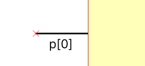
This is useful for constructing more idiomatic schematic symbols where the pin name is not typically shown - for example, in an op amp symbol:
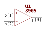
preferred-orientation
The preferred-orientation statement is used to as a hint to the schematic layout engine. It provides a set of preferred orientations of this symbol. The layout optimization engine will then try its best to keep the symbols oriented in those directions.
Signature
preferred-orientation = <SymbolOrientation>
The <SymbolOrientation> is an instance of type SymbolOrientation. There are two derived types for SymbolOrientation in the JITX runtime:
AnyRotation()- This tells the schematic layout engine that there is no preferred orientation for this component.PreferRotation(rotations:Tuple<Int>)- This allows you to specify one of four standard orientations for the schematic symbol.- Rotation Mapping:
0=>0°1=>90°2=>180°3=>270°
- Rotation Relationship:
90° * i - Each rotation is counter-clockwise around the Z-axis
- The values
0 through 3are the only accepted values.
Usage
There are many uses for this functionality, but the motivating use case is for net symbols like ground and power symbols:
public pcb-symbol altium-ground-sym :
name = "POWER-GROUND"
pin p[0] at unit-point(0.0, 0.0)
unit-line([[0.0, 0.0], [2.54, 0.0]])
unit-line(0.1, [[2.54, -1.4], [2.54, 1.4]])
unit-line(0.1, [[3.81 -0.93], [3.81, 0.93]])
unit-line(0.1, [[5.08, -0.46], [5.08, 0.46]])
unit-val([7.5, -2.5])
preferred-orientation = PreferRotation([3])
The PreferRotation([3]) results in the following preferred orientation:
Note that this rotation is about the origin in the pcb-symbol frame of reference.
Struct Statements
pcb-struct is a way to store a collection of related variables.
Example
Right now we need to use a fully qualified name to define a new pcb-struct. So if we wanted an struct named:
GenericPin
And we're defining it in a package named
defpackage ocdb/utils/property-structs
Then the struct needs to be defined as follows:
public pcb-struct ocdb/utils/property-structs/GenericPin :
max-voltage:Toleranced|RelativeVoltage ; Maximum voltage that can be applied to pin (V)
rated-esd:Double
All together this is what it looks like to define and use a
pcb-struct:
defpackage ocdb/utils/property-structs:
...
public pcb-struct ocdb/utils/property-structs/GenericPin :
max-voltage:Toleranced|RelativeVoltage ; Maximum voltage that can be applied to pin (V)
rated-esd:Double
val generic-props = GenericPin(min-max(-0.3 5.0), 1500.0)
println(max-voltage(generic-props))
When we create a value that uses a struct, the variables are given in the order defined in the pcb-struct. In the above example:
min-max(-0.3 5.0)gets assigned tomax-voltage1500.0gets assigned torated-esd
We can then access the information by the name defined in the pcb-struct. max-voltage(generic-props) fetches the value stored in the field max-voltage of a GenericPin.
JITX Types Reference
This is the reference page for JITX types.
Top Level Definitions
Top-level definitions are subtypes of JITXDef.
public deftype JITXDef <: Hashable & Equalable
;pcb-landpattern
public defstruct LandPattern <: JITXDef:
...
;pcb-pad
public defstruct Pad <: JITXDef:
...
;pcb-symbol
public defstruct SchematicSymbol <: JITXDef:
...
;pcb-rules
public defstruct Rules <: JITXDef:
...
;pcb-material
public defstruct Material <: JITXDef:
...
;pcb-board
public defstruct Board <: JITXDef:
...
;pcb-stackup
public defstruct Stackup <: JITXDef:
...
While most top-level definitions follow this format, components, modules, and bundles have additional types. Instantiables include modules and components, and since they support individual and array representations, they are subtypes of JITXDef and InstantiableType. Bundles are one of three forms that can be declared as a port in a pcb-module or pcb-component. They are subtypes of JITXDef and PortType.
public deftype InstantiableType
;pcb-module and pcb-component
public defstruct Instantiable <: JITXDef & InstantiableType:
...
public defstruct InstantiableArray <: InstantiableType:
...
public deftype PortType
public defstruct SinglePin <: PortType:
...
;pcb-bundle
public defstruct Bundle <: JITXDef & PortType:
...
public defstruct PortArray <: PortType:
...
Local Definitions
Local definitions are subtypes of JITXObject.
public deftype JITXObject <: Hashable & Equalable
;Pins of modules, components, or bundles
public defstruct Pin <: JITXObject:
...
;Land pattern pads
public defstruct LandPatternPad <: JITXObject:
...
;Symbol pins
public defstruct SymbolPin <: JITXObject:
...
;Instances of modules or components
public defstruct Instance <: JITXObject:
...
;Nets of modules
public defstruct Net <: JITXObject:
...
Self
self is an Instance than can be referenced within a pcb-module or pcb-component to access or modify fields of that definition.
JITX Patterns Cheat Sheet
The JITX language is embedded into the LB Stanza Programming Language. A comprehensive guide to learning stanza can be found in the reference, Stanza by Example. A short guide on stanza expressions and syntax can also be read here.
Common Code Patterns
for loops
A for loop takes the form
for <thing> in <sequence> <op> :
<body>
Where thing is an identifier, sequence is an expression of type Seqable, and op is an "operating" function that applies body to thing. Here are some common examples :
val values = [1, 2, 3]
for value in values do :
println(value)
; prints :
; 1
; 2
; 3
do is the most common operating expression and just applies the body of the loop to the value in the sequence.
Another common operator is filter, which is used to loop over the sequence and remove items.
val values = [1, 2, 3]
val odds =
for value in values filter :
value % 2 != 0
for odd in odds do :
println(odd)
; prints :
; 1
; 3
More examples of for loops can be found in Stanza by Example, and a list of operating functions is available in the reference.
match expressions
The match expression is a conditional expression that evaluates one of multiple branches depending on the types of its arguments. The most common form is a single argument match.
defn my-function (arg:Int|Double|True|False) :
match(arg) :
(i:Int) :
println("arg is an Int:%_" % [i])
(d:Double) :
println("arg is a Double:%_" % [d])
(b:True|False) :
println("arg is a boolean:%_" % [b])
match can take multiple arguments.
defn my-function (x:Int|Double, y:Int|Double) :
match(x, y) :
(x:Int, y:Int) :
println("x and y are Ints.")
(x:Double, y:Double) :
println("x and y are Doubles.)
(x, y) :
println("x and y are of different types!)
A common pattern is something like this :
defn my-function (arg:Int|False) :
match(arg) :
(arg:Int) :
do-something(arg)
(f:False) :
; do nothing
false
A shorthand for this syntax is
defn my-function (arg:Int|False) :
match(arg:Int) :
do-something(arg)
switch expressions
The switch expression is another conditional expression that evaluates multiple branches, it's syntactic sugar for chains of if/else if expressions.
defn arrive-or-leave (arg:String) :
switch(arg) :
"hello" :
hello()
"goodbye" :
goodbye()
else :
fatal("The caller has bad manners.")
supports statements
Supports statements declare what bundle(s) a component or module supports and how the bundle pins are mapped to the ports of the component or module.
; Bundles may be used inside pcb-components or
; pcb modules
; The mapping goes
; bundle.pin-ref => self.pin-ref
supports bundle :
bundle.p[1] => self.p[2]
; ... rest of mappings to the bundle ...
requires statements
Requires statements are used in pcb-module definitions to define what supports they need.
; inside pcb-module
require <ref> : <bundle> from <instance>
The pin solver will automatically map pins that supports the bundle that the module requires to an alias, ref.
In addition to using require inside of a pcb-module, require statements can be "chained" inside of supports statements.
pcb-component mcu :
port p: pin[128]
for n in 10 to 30 do :
supports gpio :
gpio.p => self.p[n]
supports spi-controller():
require io : gpio[4]
spi-controller().copi => io[0].p
spi-controller().cipo => io[1].p
spi-controller().cs => io[2].p
spi-controller().sck => io[3].p
pin-properties tables
pin-properties tables are a mechanism for declaring metadata about the pins in a pcb-component. It is used for commands like assign-landpattern, assign-symbol, and make-box-symbol.
; Declare pin properties: the names of pins and pads they are mapped
; to on the associated landpattern
pcb-component component :
;Each row has format:
pin-properties :
[pin:Ref | pads:Int ... ]
[a | 1 ]
[b | 2 ]
[c | 3 ]
[gnd | 4 5 6 7 8 ]
[d+ | 9 ]
[d- | 10 ]
make-box-symbol()
assign-landpattern(mylandpattern)
pcb-component definitions
See the reference for more.
pcb-component component :
name = "My awesome component"
mpn = "MPN"
manufacturer = "Manufacturer"
description = "This is an example component."
; ... component statements ...
pcb-module definitions
See the reference for more.
pcb-module module :
; Define some metadata of the module
name = "My Module"
description = "This is an example module"
; Declare some ports
port io: bundle
; Declare some instances
inst U: component
; Net ports and instances together
net (io.p[1], U.p[1])
; Perhaps add some layer geometry
layer(Silkscreen("F-Silk", Top)) = Text("REV 1.0", 2.54, C, loc(0.0, 0.0))
; Add instances to schematic groups
schematic-group(U) = grouped-insts
; Add the instances to schematic groups
pcb-landpattern definitions
See the reference for more.
pcb-landpattern my-landpattern :
; define a pad
pad p[1] : smd-pad(Circle(1.0)) at loc(0.0, 0.0) on Top
; Add custom soldermask layers
layer(SolderMask(Top)) = Rectangle(1.25, 1.25)
pcb-component to pcb-symbol mappings
Symbol pins are mapped to component pins using the following syntax :
pcb-component my-resistor :
port p: pin[[1, 2]]
; sym is an expression corresponding to a generated
; pcb-symbol
val sym = resistor-sym()
; The mapping is:
; <component-pin> => <symbol>.<symbol-pin>
symbol =
sym(p[1] => sym.p[1],
p[2] => sym.p[2])
pcb-component to pcb-landpattern mappings
Landpattern pins are mapped to component pins using the following syntax :
pcb-component my-resistor :
port p: pin[[1, 2]]
; lp is an expression corresponding to a generated
; pcb-landpattern
val lp = ipc-two-pin-landpattern("0201")
; The mapping is:
; <component-pin> => <landpattern>.<landpattern-pad>
landpattern =
lp(p[1] => lp.p[1],
p[2] => lp.p[2])
Getting and setting properties
; set a property
property(self.property-name) = expression
; get a property
val property = property(self.property-name)
; check if a property is set
has-property?(self.property-name)
; optionally check if a property is set and
; perform some logic with the value
match(property?(self.property-name)) :
(one:One) :
val property = value(one)
(none:None) :
; property is not set
Adding passive components
ocdb/utils/generic-components has a few generators for querying jellybean components from
the JITX parts database. See the design variables reference for configuration with
global design parameters.
defpackage my-design :
import jitx
import jitx/commands
import ocdb/utils/design-vars
import ocdb/utils/generic-components
; define the minimum package size for the design
MIN-PKG = "0601"
pcb-module module :
; Drop some passives in a module
; Query a generic 1k ohm chip resistor
inst R1 : chip-resistor(1.0e3)
; Query a generic 1k ohm chip resistor with 5% tolerance
inst R2 : chip-resistor(1.0e3, 0.05)
; Query a generic 4.7nF ceramic cap
inst C1 : ceramic-cap(4.7e-9)
; Query a generic 4.7nF ceramic cap with 5% tolerance
inst C1 : ceramic-cap(4.7e-9)
Named nets
Nets can be given a name, but it must have one character of whitespace between the name and arguments!
pcb-module module :
net name (a, b, c)
; net name(a, b,c) <--- invalid!
Learning Stanza: quick reference
JITX is implemented in the LB Stanza (Stanza) programming language. We like stanza because it supports types to help write correct code, and also allows higher-level programming. We can write Stanza programs inline with JITX code, to generate designs, components, and modules programmatically.
We do not need all of Stanza to develop with JITX; this document provides a short walkthrough of commonly-used Stanza features.
Comments
; this is a comment
;<A>
This is a block comment
;<B>
block comments can be nested with optional tags.
;<B>
;<A>
Basics
defpackage learn-stanza-in-y:
import core
import collections
;=========================================================================
; The basics, things you'd find in most programming languages
;=========================================================================
; Variables can be mutable (var) or immutable (val)
var mutable = "this one can be"
val immutable = "this string can't be changed"
; The basic data types (annotations are optional)
val an-int: Int = 12345
val a-long: Long = 12345L
val a-float: Float = 1.2345f
val a-double: Double = 3.14159
val a-string: String = "this is a string"
val a-multiline-string = \<tag>
this is a multi-line string literal.
<tag>
; print formatted strings with println() and "..." % [...]
println("this is a formatted string %_ %_" % [mutable, immutable])
; Stanza is optionally typed, and has a ? (any) type.
var anything:? = 0
anything = 3.14159
anything = "a string"
; Stanza has basic collections such as Tuples, Arrays, Vectors, HashTables, etc.
val tuple: Tuple<?> = [mutable, immutable]
val array = Array<?>(3)
array[0] = "string"
array[1] = 1
array[2] = 1.23455
; array[3] = "out-of-bounds" ; arrays are bounds-checked
val vector = Vector<?>()
vector[0] = "string"
vector[1] = 1
vector[2] = 3.14159
val hash-table = HashTable<String, ?>()
hash-table["0"] = 0
hash-table["1"] = 1
hash-table["2"] = 1
Functions
; Functions are declared with the `defn` keyword
defn my-function (arg:?) : ; note the space between identifier and arg list
println("called my-function with %_" % [arg])
my-function("arg") ; note the lack of a space to call the function
; If you try to define a function without a space, the syntax highlighter
; should give you a gentle nudge to fix it (ie, the red text and underline)
defn invalid-func(arg1, arg2) -> Int:
...
; functions can be declared inside another function and capture their environment. This is called a closure.
defn outer (arg):
defn inner ():
println("outer had arg: %_" % [arg])
inner()
outer("something")
; functions are "first-class" in stanza, meaning you can assign variables
; to functions and pass functions as arguments to other functions.
val a-function = outer
defn do-n-times (arg, func, n:Int):
for i in 0 to n do :
func(arg)
do-n-times("argument", a-function, 3)
; sometimes you want to define a function inline, or use an anonymous function.
; for this you can use the syntax:
; fn (args):
; ...
do-n-times("hello", fn (arg): println(arg), 2)
; there is a shorthand for writing anonymous functions, the above can be written
do-n-times("hello", { println(_) }, 2)
; the short hand works for multiple arguments as well.
val multi-lambda = { println(_ + 2 * _) }
multi-lambda(1, 2)
; You can reference the arguments explicitly as well
; with `_0`, `_1`, for the `Nth` argument.
val lambda-args = { println(_0, + (3 * _1)) }
User Defined Types
; Structs are declared with the `defstruct` keyword
defstruct MyStruct:
field:String
; constructors are derived automatically
val my-struct = MyStruct("field:value")
; fields are accessed using function-call syntax
println(field(my-struct))
; Stanza supports subtyping with a "multimethod" system based on method
; overloading.
;
; This effectively defines an interface for type `Mytype` consisting
; of a single method `a-method`
deftype MyType
defmulti a-method (m:MyType)
defstruct Foo <: MyType:
fab:Int
defmethod a-method (a-foo: Foo):
println("called a-method on a Foo")
defstruct Bar <: MyType:
bab:Double
defmethod a-method (a-foo: Bar):
println("called a-method on a Bar")
The Type System
; True and False are types with a single value.
val a-true: True = true
val a-false: False = false
; You can declare a union type, or a value that is one of a set of types
val a-boolean: True|False = true
val another-boolean: True|False = false
; You can pattern match on types
match(a-boolean):
(t:True): println("is true")
(f:False): println("is false")
; You can match against a single possible type
match(a-boolean:True):
println("is still true")
else:
println("is not true")
; You can compose program logic around the type of a variable
if anything is Float :
println("anything is a float")
else if anything is-not String :
println("anything is not an int")
else :
println("I don't know what anything is")
Control Flow
; stanza has the standard basic control flow
val condition = [false, false]
if condition[0] :
; do something
false
else if condition[1] :
; do another thing
false
else :
; whatever else
false
; there is also a switch statement, which can be used to pattern match
; on values (as opposed to types)
switch(anything):
"this": false
"that": false
"the-other-thing": false
else: false
; for and while loops are supported
while condition[0]:
println("do stuff")
; More on For Loops shortly.
for i in 0 to 10 do:
vector[i] = i
; stanza also supports named labels which can functin as break or return
; statements
defn another-fn ():
label<False> return:
label<False> break:
while true:
if condition[0] is False:
break(false)
return(false)
; Stanza has exceptions and provides a syntax similar to Python:
try:
some-func()
throw(Exception("Abort!"))
catch (e:Exception):
println("Error: %~" % [e])
finally:
println("We made it!")
; For a comprehensive guide on Stanza's advanced control flow, check out
; this page: http://lbstanza.org/chapter9.html from Stanza-by-Example
For Loop Operators
; The for-loop has a special expression at the end called the "Operating Function"
; In most cases - it is simply the `do` operator:
for i in 0 to 10 do:
println("Index: %_" % [i])
; However the operating function can _do_ so much more!
; Operating functions typically have the form:
defn some-op (func, xs:Seqable) -> False:
...
; Here the first argument is a function, and the second argument
; is a sequence of objects
; Referring to our previous example:
for i in 0 to 10 do:
println("Index: %_" % [i])
; When used in a for-loop, the body of the for-loop becomes the function
; `func`.
defn body (i) -> False :
println("Index: %_" % [i])
; The value `i` becomes the argument to `func`. The expression `0 to 10` becomes `xs`.
; There are many operating functions - `seq`, `map`, `filter`, etc. - defined in the stanza core library.
; https://lbstanza.org/reference.html#anchor478
Sequences
; for "loops" are sugar for a more powerful syntax.
val xs = [1, 2, 3]
val ys = ['a', 'b', 'c']
val zs = ["foo", "bar", "baz"]
for (x in xs, y in ys, z in zs) do :
println("x:%_, y:%_, z:%_" % [x, y, z])
;xs, ys, and zs are all "Seqable" meaing they are Seq types (sequences).
; Sequences are called "iterators" in other languages, like Python, and
; provide similar abstractions.
;
; A common sequence task is concatenating sequences. This is accomplished
; using the `seq-cat` operating function. This is analogous to
; "flattening" iterators
val concat = to-tuple $
for sequence in [xs, ys, zs] seq-cat:
sequence
; we can also use a variation to interleave the elements of multiple sequences
val interleaved = to-tuple $
for (x in xs, y in ys, z in zs) seq-cat :
[x, y, z]
println("[%,] [%,]" % [concat, interleaved])
; Another common task is mapping a sequence to another, for example multiplying
; all the elements of a list of numbers by a constant. To do this we use `seq`.
var numbers = [1.0, 2.0, 3.0, 4.0]
numbers = to-tuple $
for n in numbers seq :
2.0 * n
println("%," % [numbers])
if find({_ == 2.0}, numbers) is-not False :
println("found it!")
; or maybe we just want to know if there's something in a sequence
var is-there = for n in numbers any? :
n == 2.0
; since this is "syntactic sugar" we can write it explicitly using an
; anonymous function
is-there = any?({_ == 2.0}, numbers)
Documentation
;=========================================================================
; Documentation
;=========================================================================
;
; Top level statements can be prefixed with the "doc" field which takes
; a string value and is used to autogenerate documentation for the package.
doc: \<doc>
# Document Strings
```stanza
val you-can = "include code snippets, too"
```
To render documentation as markdown (compatible with mdbook)
```bash
stanza doc source.stanza -o docs
```
<doc>
defn docfn () : false
API Reference for the jitx/commands package
Part Query API
Main Design
Top Level Commands
Lookup
Part Query API
The part query API is a low level API that returns actual components that meet the specified criteria.
We recommend using the Higher level Part Query accessors to query for parts.
The JITX database currently supports 4 categories. Detailed information on how to query each category can be found at:
The API queries the JITX database containing millions of parts and supports:
- filtering on attributes by equality, inequality or set of values,
- optimizing on an attribute (for example smallest area or price),
- querying for a specific number of parts
- requiring some attributes to exist in the resulting parts (for example tolerance)
- listing the available values for an attribute after filtering on other query parameters
- integrate real-time sourcing data to the query
Part query results are cached in memory for future use. This can be particularly useful when using the jitx repl.
The cache is lost when a jitx program exits.
Caching
Internet is required to perform the part queries the first time. All results are then cached to disk to be reused across sessions. To query fresh parts, clear the cache with:
stanza> import jitx/commands
stanza> clear-dbquery-cache()
Accessors
The part query API is imported from the package jitx/commands. Here are the accessors:
public defn dbquery (params: Tuple<KeyValue<String, Tuple<String>|Tuple<Double>|String|Double|Int>>, limit: Int) -> Tuple<JSON>
The maximum number of components that can be queried at a time by dbquery is 1000.
Any value of limit in dbquery above 1000 will throw an error.
public defn dbquery-all (params: Tuple<KeyValue<String, Tuple<String>|Tuple<Double>|String|Double|Int>>) -> Tuple<JSON>
dbquery-all calls dbquery with a limit of 25.
As our part database contains millions of resistors and hundreds of thousands of inductors and capacitors,
dbquery-all cannot return all components that meet the query.
public defn dbquery-first (args: Tuple<KeyValue<String, Tuple<String>|Tuple<Double>|String|Double|Int>>) -> JSON
dbquery-first calls dbquery with a limit of 1, if no component is found, it throws a NoComponentMeetingRequirements
Examples
Querying the smallest 1Ω resistor:
stanza> import jitx/commands
stanza> val resistor-json = dbquery-first(["category" => "resistor", "resistance" => 1.0, "_sort" => ["area"]])
stanza> println(resistor-json)
JObject(entries = ["_id" => "0f3e3eeb6393f83d591a03c3" "trust" => "low" "category" => "resistor" "mpn" => "CRCW01001R00FYEL" "mounting" => "smd" "manufacturer" => "Vishay Dale" "type" => "chip" "dimensions" => JObject(entries = ["x" => 0.4 "y" => 0.2 "z" => 0.15 "area" => 0.08]) "stock" => 9355.0 "minimum_quantity" => 1.0 "metadata" => JObject(entries = ["datasheets" => "https://www.vishay.com/docs/20056/crcw01005e3.pdf" "image" => "//media.digikey.com/Renders/Vishay%20Dale%20Renders/CRCW-01005-(0402metric).jpg" "digi-key-part-number" => "541-4281-6-ND" "description" => "RES SMD 1 OHM 1% 1/32W 01005" "factory-stock" => 0.0 "unit-price" => "Digi-Reel" "qty" => 0.0 "packaging" => "Digi-Reel®" "series" => "CRCW" "supplier-device-package" => 1005.0 "number-of-terminations" => 2.0]) "tolerance" => JObject(entries = ["min" => -0.01 "max" => 0.01]) "resistance" => 1.0 "rated-power" => 0.03 "composition" => "thick-film" "tcr" => JObject(entries = ["pos" => -0.0002 "neg" => 0.0006]) "rated-temperature" => JObject(entries = ["min" => -55.0 "max" => 125.0]) "case" => "01005" "update_date" => "2021-09-04T01:35:34.335000"])
stanza> import ocdb/utils/db-parts
stanza> import json
stanza> println $ Resistor(resistor-json as JObject)
Resistor(
mpn = CRCW01001R00FYEL
trust = low
(x, y, z) = (0.4, 0.2, 0.15)
mounting = smd
rated-temperature = MinMaxRange(min=-55.0, max=125.0)
case = 01005
type = chip
tolerance = MinMaxRange(min=-0.01, max=0.01)
resistance = 1.0
composition = thick-film
rated-power = 0.03
TCR = TCR(positive=-0.0002, negative=0.0006)
sourcing = ESR(price=false, minimum-quantity=1, stock=9355)
metadata =
"datasheets" => "https://www.vishay.com/docs/20056/crcw01005e3.pdf"
"image" => "//media.digikey.com/Renders/Vishay%20Dale%20Renders/CRCW-01005-(0402metric).jpg"
"digi-key-part-number" => "541-4281-6-ND"
"description" => "RES SMD 1 OHM 1% 1/32W 01005"
"factory-stock" => 0.0
"unit-price" => "Digi-Reel"
"qty" => 0.0
"packaging" => "Digi-Reel®"
"series" => "CRCW"
"supplier-device-package" => 1005.0
"number-of-terminations" => 2.0)
Querying some capacitors (at most 25 by default):
$ jitx repl
stanza> import jitx/commands
stanza> val capacitor-jsons = dbquery-all(["category" => "capacitor"])
Querying 200 inductors with 1µH inductance:
$ jitx repl
stanza> import jitx/commands
stanza> val inductor-jsons = dbquery(["category" => "inductor", "inductance" => 1.0e-6], 200)
Querying the list of available mcu cores in the JITX database:
$ jitx repl
stanza> import jitx/commands
stanza> val cores = dbquery-all(["category" => "microcontroller", "_distinct" => "core"])
stanza> println(cores)
["ARM Cortex-M0" "ARM Cortex-M0+" "ARM Cortex-M3" "ARM Cortex-M4" "ARM Cortex-M7"]
Querying the list of available packages for smd resistors:
$ jitx repl
stanza> import jitx/commands
stanza> println $ dbquery-all(["category" => "resistor" "mounting" => "smd", "_distinct" => "case"])
[JNull() "009005" "01005" "0201" "02016" "0202" "0302" "0303" "0402" "0404" "0503" "0505" "0603" "0612" "0805" "1206" "1210" "1218" "1812" "2-SMD, J-Lead" "2010" "2010 J-Lead" "2012 J-Lead" "2015" "2512"]
Creating a module with the cheapest smd resistor with a resistance of 1Ω±5%:
#use-added-syntax(jitx)
defpackage my-design :
import jitx/commands
pcb-module my-module :
inst resistor : dbquery-first(["resistance" => 10.0 "tolerance" => 0.05 "mounting" => "smd" "_sort" => ["cost"]])
Querying the list of packages available for mcus:
$ jitx repl
stanza> import jitx/commands
stanza> val packages = dbquery-all(["category" => "microcontroller" "_distinct" => "mfg-package"])
stanza> println(length(packages))
28
stanza> println(packages)
["LFBGA100" "LQFP100" "LQFP144" "LQFP176" "LQFP208" "LQFP48" "TFBGA216" "TFBGA225" "TFBGA64" "UFBGA100" "UFBGA132" "UFBGA169" "UFBGA64" "UFQFPN28" "UFQFPN32" "UFQFPN48" "WLCSP100" "WLCSP104" "WLCSP156" "WLCSP168" "WLCSP180" "WLCSP25" "WLCSP36" "WLCSP49" "WLCSP63" "WLCSP64" "WLCSP81" "WLCSP90"]
Querying the list of mcu mpns for package "WLCSP49":
$ jitx repl
stanza> import jitx/commands
stanza> val mpns = dbquery(["category" => "microcontroller" "mfg-package" => "WLCSP49" "_distinct" => "mpn"], 500)
stanza> println(length(mpns))
21
stanza> println(mpns)
["STM32F071CBY6" "STM32F071CBY7" "STM32F072CBY6" "STM32F072CBY7" "STM32F078CBY6" "STM32F303C8Y6" "STM32F318C8Y6" "STM32F334C8Y6" "STM32F334C8Y7" "STM32F411CCY6" "STM32F411CCY7" "STM32F411CEY6" "STM32F411CEY7" "STM32L071CBY6" "STM32L071CBY7" "STM32L071CZY6" "STM32L071CZY7" "STM32L073CZY6" "STM32L073CZY7" "STM32L082CZY6" "STM32L082CZY7"]
Querying the list for all bundles for all mcus with the package "WLCSP49":
$ jitx repl
stanza> import jitx/commands
stanza> val mcus = dbquery(["category" => "microcontroller" "mfg-package" => "WLCSP49"], 500)
stanza> println(length(mcus))
21
stanza> import json
stanza> println $ to-tuple $ to-hashset<String> $ for mcu in (mcus as Tuple<JObject>) seq-cat : mcu["bundles"] as Tuple<String>
["RCC_OSC32_OUT" "USART3_RTS" "I2S1_CK" "SPI1_SCK" "RCC_OSC_OUT" "USART4_RTS" "LPUART1_DE" "LPUART1_CTS" "SPI2_SCK" "USART5_RTS" "SPI3_SCK" "SPI4_SCK" "LPUART1_TX" "SPI5_SCK" "SYS_JTDO-SWO" "I2S5_SD" "LPUART1_RX" "I2S4_SD" "I2S3_SD" "I2C1_SDA" "I2S2_SD" "I2C2_SDA" "I2S1_SD" "I2C3_SDA" "SYS_SWCLK" "SYS_JTDO-TRACESWO" "SPI5_MISO" "SPI5_MOSI" "SPI4_MISO" "SPI4_MOSI" "USART1_CTS" "USART5_DE" "SPI3_MISO" "SPI3_MOSI" "USART2_CTS" "I2S5_WS" "LPUART1_RTS" "USART4_DE" "SPI2_MISO" "SPI2_MOSI" "USART3_CTS" "I2S4_WS" "USART3_DE" "USART6_TX" "SPI1_MISO" "SPI1_MOSI" "USART4_CTS" "RCC_OSC_IN" "I2S3_WS" "USART2_DE" "USART5_TX" "RCC_OSC32_IN" "I2S2_WS" "CAN_TX" "SPI1_NSS" "USART1_DE" "USART4_TX" "USART6_RX" "SYS_SWDIO" "I2C1_SCL" "I2S1_WS" "SPI2_NSS" "USART3_TX" "USART5_RX" "SYS_JTCK-SWCLK" "I2C2_SCL" "CAN_RX" "SPI3_NSS" "USART2_TX" "USART4_RX" "I2C3_SCL" "SPI4_NSS" "USART1_TX" "USART3_RX" "USART5_CK" "SPI5_NSS" "USART2_RX" "USART1_RX" "USART3_CK" "USART2_CK" "SYS_JTMS-SWDIO" "USART1_CK" "I2S5_CK" "I2S1_MCK" "I2S4_CK" "I2S2_MCK" "USART1_RTS" "I2S3_CK" "I2S3_MCK" "USART2_RTS" "I2S2_CK"]
Supported parameters
The supported special query parameters are:
- _exist : List of attributes that the returned documents must contain.
- _sort : The returned documents will be sort according to the list of attributes specified
by this parameter, applied in the order they appear. Sorting in descending fashion can
be obtained by starting a sorting attribute by a minus sign "−". This can take 2 additional value besides
the list of existing properties:
areais an alias fordimensions.areaandcostis an alias forprice. - _distinct : If this parameter exist, it must be an attribute string, the query will return the set of available values for the specified attribute in the list of documents that meet all the query constraints.
Regular filter properties:
- We can filter on a part attribute :
{"category": "resistor"}. - We can filter on a capacitance, resistance and inductance, those constraints are replaced by interval allowing for queries with a precision of 0.0005Ω, 0.01A and 0.01F respectively.
- We can filter on a tolerance :
{"tolerance": 0.05}will constrain the tolerance to be an exact match{"tolerance": {"min": -0.05, "max": 0.05}}. Returns500 Bad Requestif this is not a positive double - We can filter on a nested parameter using
.:{"dimensions.x": 11} - We can filter on a list of values giving a list :
{"case": ["Axial", "0402"]} - We can filter with an inequality prepending
min-ormax-:{"max−rated-power": 0.05}. max-x,max-yandmax-zare shorthands formax-dimensions.x,max-dimensions.y,max-dimensions.z- We interpret
minimum_quantityas a floor on bulk purchase size; we automatically convertminimum_quantitytomax-minimum_quantity.
Typo checker
The typo checker is triggered when an unsupported parameter is used in a query where the "category" parameter is present and amongst ["resistor", "capacitor", "inductor", "microcontroller"]. When the typo checker detects an unsupported parameter, it will throw an error printing the list of supported parameters of the category. Example:
$ jitx repl
stanza> import jitx/commands
stanza> println $ dbquery-all(["category" => "capacitor" "typo" => 1.0e-06])
The invalid attributes ("typo") are used in the query ["category" => "capacitor" "typo" => 1.0e-06].
Valid attributes for category capacitor must be amongst:
- anode
- capacitance
- case
- category
- dimensions.area
- dimensions.x
- dimensions.y
- dimensions.z
- electrolyte
- esr
- esr_frequency
- manufacturer
- minimum_quantity
- mounting
- mpn
- price
- rated-current-pk
- rated-current-rms
- rated-temperature.max
- rated-temperature.min
- rated-voltage
- rated-voltage-ac
- stock
- temperature-coefficient.change
- temperature-coefficient.code
- temperature-coefficient.lower-temperature
- temperature-coefficient.raw_data
- temperature-coefficient.tolerance
- temperature-coefficient.upper-temperature
- temperature-coefficient.value
- tolerance
- tolerance.max
- tolerance.min
- trust
- type
- update_date
Sourcing data
If the request contains the attributes _stock or/and _sellers:
more advanced part sourcing data will be independently queried and integrated to the results, disregarding sellers that:
- are not in the list
- do not have an inventory level above the queried stock
- do not have a pricing offering with a minimum quantity lower that the queried stock In this case, any part that does not have sourcing data that meets the criteria above will be ignored.
If _stock is 0 or _sellers is [], then no filtering out is done using those properties. In particular querying with
both [_"stock" => 0, "_sellers" => []] will append the whole part sourcing data to the result for any sellers at any inventory
stock and with any price offerings.
We recommend to always provide a list of allowed sellers as the part sourcing data contains unverified sellers that may be intermediaries.
A sellers key will be added to the returned json with the sourcing data meeting the request.
The best price from each seller is aggregated in the resolved_price key in each seller data.
The best price from all qualifying offerings is returned in the resolved_price key at the root of the json.
"sellers": [
{
"company_name": ...,
"resolved_price": ...,
"offers": [{
"inventory_level": ...,
"prices": [{"quantity": ..., "converted_price": ...}]
},...]
}
]
"resolved_price": ...
Sorting by price
cost and price can be used used interchangeably. We are using cost in what follows.
If _sort is ["cost"] (respectively ["-cost"]), results will be sorted by increasing (respectively decreasing) price.
If neither _stock nor _sellers are parameters of the query, then the price used to sort on for resistors, capacitors and resistors
is the price for 1 unit from Digikey (updated every week). For the microcontroller category, no sorting on price will occur, please see
the next section.
If _stock or _sellers are parameters of the query, then real-time sourcing data is integrating in the query (see section "Sourcing data" above).
At most 1000 parts meeting the query are retrieved from the JITX database, then sourcing data for each part is retrieved,
the price used to sort on is the resolved_price attribute.
Utilities
This section contains info on JITX utility functions.
Stateful
Stateful is a useful tool for managing property states.
Data Types
public defstruct Stateful<K,V> :
current: K|False
states: Tuple<KeyValue<K,V>>
public defn Stateful<?K,?V> (states:Seqable<KeyValue<?K, ?V>>) -> Stateful
public defn Stateful<?K,?V> (current:JITXValue, states:Seqable<KeyValue<?K, ?V>>) -> Stateful
Stateful is a collection of states with a possibly current state.
current: the current state, or false if there is no current state.states: mappings from a state's name to a value.
Function
public defn get<?K,?V> (s:Stateful<?K,?V>, state:?K) -> V :
Returns the value for the given state.
public defn state-names<?K,?V> (s:Stateful<?K,?V>) -> Tuple<K> :
Returns the names of all states.
Additional Syntaxes
state(<object>.<property>) = <state>
Set the property's state to state. It is required that object.property is a Stateful. This statement must be declared inside a pcb-module, pcb-component, or support option.
state(<object>.<property>)
Get the property's current state. It is required that both object.property is a Stateful and there is a current state.
state?(<object>.<property>)
Get the property's current state. It is required that object.property is a Stateful. Returns false if there is no current state.
has-state?(<object>.<property>, <state>)
Returns whether state is one of object.property's states. It is required that object.property is a Stateful.
pcb-module main :
port p : pin[5]
;Assign a Stateful property to pin p[3] in a USB-powered system.
;The low state load-current is 100mA and the high state load-current is 1.5A.
;No initial state is assigned.
property(p[3].load-current) = Stateful(["low" => 100.0e-3,
"high" => 1.5])
;Get a list of state names. Returns`["low" "high"]`
state-names(property(p[3].load-current))
;Try getting the current state. Returns false.
state?(p[3].load-current)
;Set the state to "low".
;Much like properties, states can be set inside a module, component, or support option.
state(p[3].load-current) = "low"
;Get the current state. Returns "low".
state(p[3].load-current)
;Does the property have a "high" state? Returns true.
has-state?(p[3].load-current, "high")
The above pcb-module demonstrates how all syntaxes can be used.
Toleranced
Toleranced is a useful tool for managing values with some tolerance.
Data Types
public defstruct Toleranced :
typ: Double
tol+: Double
tol-: Double
Toleranced is a generic value with upper and lower bound tolerances that may be off-center (upper tolerance != lower tolerance). It represents the inequality (typ - tol-) <= T <= (typ + tol+).
typ: the typical valuetol+: the upper tolerancetol-: the lower tolerance
Functions
public defn min-typ-max (min:Double, typ:Double, max:Double) -> Toleranced
Creates a Toleranced value from minimum/typical/maximum values.
public defn min-max (min:Double, max:Double) -> Toleranced
Creates a Toleranced value from minimum/maximum values with typ as the midpoint.
public defn tol% (typ:Double, tol+:Double, tol-:Double) -> Toleranced
Creates a Toleranced value using percentages (0.0 <= tol+/tol- <= 100.0) for +/- tolerance.
public defn tol% (typ:Double, tol:Double) -> Toleranced
Creates a symmetric Toleranced value using percentages (0.0 <= tol <= 100.0) for +/- tolerance.
public defn tol (typ:Double, tol+:Double, tol-:Double) -> Toleranced
Creates a Toleranced value using relative values for +/- tolerance.
public defn tol (typ:Double, tol:Double) -> Toleranced
Creates a Toleranced value using the symmetric range for +/- tolerance.
public defn tol+% (t:Toleranced) -> Double
Returns the upper tolerance, as a percentage.
public defn tol-% (t:Toleranced) -> Double
Returns the lower tolerance, as a percentage.
public defn max-value (t:Toleranced) -> Double
Returns the maximum value of the tolerance.
public defn typ-value (t:Toleranced) -> Double
Returns the typ value of the tolerance (not necessarily the center value).
public defn min-value (t:Toleranced) -> Double
Returns the minimum value of the tolerance.
public defn center-value (t:Toleranced) -> Double
Returns the center value of the tolerance, which may not be the typical value.
public defn in-range? (t:Toleranced, value:Double) -> True|False
Checks if a value is within the tolerance's range.
public defn in-range? (t:Toleranced, value:Toleranced) -> True|False
Checks if a value Toleranced min/max is within the first argument tolerance's min/max.
public defn tolerance-range (t:Toleranced) -> Double
Returns the difference between maximum and minimum values of the tolerance.
public defn minus (a:Toleranced, b:Toleranced) -> Toleranced
public defn minus (a:Double, b:Toleranced) -> Toleranced
Subtraction of Toleranced values. Arithmetic with Toleranced values are useful for the worst case analysis, but be aware the bounds can grow quickly so it's important to use realistic ranges.
public defn plus (a:Toleranced, b:Toleranced) -> Toleranced
public defn plus (a:Double, b:Toleranced) -> Toleranced
Addition of Toleranced values. See note under toleranced subtraction.
public defn divide (a:Toleranced, b:Toleranced) -> Toleranced
public defn divide (a:Double, b:Toleranced) -> Toleranced
Division of Toleranced values. See note under toleranced subtraction.
public defn times (a:Toleranced, b:Toleranced) -> Toleranced
public defn times (a:Double, b:Toleranced) -> Toleranced
Multiplication of Toleranced values. See note under toleranced subtraction.
Example usage
; Create a range between -0.3 and 5.0
val range-1 = min-max(-0.3, 5.0)
; Create a range within 20% of 500.0
val range-2 = tol%(500.0, 20.0)
; Check if range-2 includes range-1
in-range?(range-2, range-1)
; Get the minimum value of range-1
min-value(range-1)
ocdb/utils/design-vars
Design variables are configuration settings for OCDB applied to the current design (or sets of designs, in multi-board projects). These variables control generator mechanisms across OCDB.
Data Types
public pcb-enum ocdb/utils/design-vars/DensityLevel:
DensityLevelA
DensityLevelB
DensityLevelC
DensityLevel is a helper enum that represents the desired density level of the current design (A, B, or C, with "A" being the least dense and "C" being the most dense). It is used to generate IPC compliant land patterns.
Global Variables
public var OPERATING-TEMPERATURE = min-max(0.0, 25.0)
The operating temperature range of the design (C).
public var OPTIMIZE-FOR = ["area"]
The desired optimization approach by JITX internal generators. Supported values are "area" and "cost".
public var MAX-Z = 500.0
The maximum height of a component (mm).
public var MIN-PKG = "0201"
The minimum package size of a passive component. Used to find components that can be placed by the fabricator when pulling components from the JITX database.
public var APPROVED-DISTRIBUTOR-LIST = ["Allied Electronics & Automation"
"Arrow Electronics"
"Avnet"
"Digi-Key"
"Future Electronics"
"Mouser"
"Newark"]
The list of approved distributors. Set it to false to allow any distributor.
public var DESIGN-QUANTITY = 100
The number of boards you intend to fabricate. Used to find components in stock when pulling components from the JITX database.
public var ALLOW-NON-STOCK = true
Whether to allow components to be out of stock. JITX gives warning messages when components are out of stock and ALLOW-NON-STOCK is true (the default bevavior). If ALLOW-NON-STOCK is false, JITX throws an exception when any component is out of stock.
public var PREFERRED-MOUNTING = "smd"
The preferred mounting style of a component pulled from the JITX database. Supported values are ["smd", "through-hole"].
public var MIN-CAP-VOLTAGE = 10.0
Minimum voltage to allow for capacitors
public var DEFAULT-ALLOW-ALL-VENDOR-PART-NUMBERS = false
Use all parts from the Parts Database for existing parametric queries (e.g. chip-resistor). If false, restrict these queries to a set of parts with a higher confidence in quality.
public var DENSITY-LEVEL: DensityLevel = DensityLevelC
The preferred density level of the design. Used when generating land patterns.
public var MIN-SOLDER-MASK-SLIVER: Double = 0.15
The minimum space allowed between non overlapping regions of solder mask opening. Used when checking land patterns.
public var MIN-OUTER-LAYER-PAD-SIZE: Double = 0.2032
The minimum size of a circular pad on the outer layers. Used when computing through hole land patterns.
public var MAX-HOLE-SIZE-TOLERANCE: Double = 0.0508
The board fabricator's tolerance on the diameter of the largest hole (mm). Used when computing through hole land patterns.
public var MIN-HOLE-SIZE-TOLERANCE: Double = 0.0508
The board fabricator's tolerance on the diameter of the smallest hole (mm). Used when computing through hole land patterns.
public var HOLE-POSITION-TOLERANCE: Double = 0.0508
The board fabricator's tolerance on placing the center of any hole (mm). Used when computing through hole land patterns.
ocdb/utils/landpatterns
Land patterns (sometimes called footprints) are the geometry associated with a single package that is to be placed on a design. In JITX, they are represented using the pcb-landpattern statement. The package ocdb/utils/landpatterns contains utilities for generating optimized land-patterns from parameters.
Table of Contents
- Helpful References
- Definitions
- Two Pin Land Patterns
- Small Outline (SO) Land Patterns
- QFP Land Patterns
- QFN Land Patterns
- BGA Land Patterns
Helpful References
- JEDEC JESD30E, "Descriptive Designation System for Semiconductor-device packages"
- IPC 7351B, Generic Requirements for Surface Mount Design and Land Pattern Standard
Definitions
- Package: the physical device that will be placed (including the exterior plastic packaging and metal leads or terminations of a component). A package has one or more leads or terminations..
- Lead or Termination: The conductors on the package that interface with the electrical device.
- Land Pattern: the geometry on the layers of the board that sits underneath the package. A landpattern has one or more pads or and zero or more layers.
- Pad: the geometry on the layers associated with a single lead or termination of the component.
Two Pin Land Patterns
Chip Land Patterns
Two pin chip land patterns are commonly used for passive devices. The following generators are used to generate land patterns for these components that are compliant with IPC specifications.
public defn make-two-pin-chip-landpattern (length:Toleranced,
width:Toleranced,
lead-length:Toleranced)
Create a two pin surface mount (chip) non-polarized land pattern.
length: the length of the component.width: the width of the component.lead-length: the length of the leads of the component.
public defn make-two-pin-chip-landpattern (length:Toleranced,
width:Toleranced,
lead-length:Toleranced,
polarized?:True|False)
Create a two pin surface mount (chip) land pattern with optional polarization
length: the length of the component.width: the width of the component.lead-length: the length of the leads of the component.polarized?:trueif the land pattern is polarized,falseotherwise.
public defn make-two-pin-chip-landpattern (length:Toleranced,
width:Toleranced,
lead-length:Toleranced,
lead-width:Toleranced)
Create a two pin surface mount (chip) land pattern with a lead width that is different from the component width.
length: the length of the component.width: the width of the component.lead-length: the length of the leads of the component.lead-width: the width of the leads of the component, which may be different than the width of the component.
public defn make-two-pin-chip-landpattern (length:Toleranced,
width:Toleranced,
lead-length:Toleranced,
lead-width:Toleranced,
polarized?:True|False)
Create a two pin surface mount (chip) land pattern with a lead width that is different from the component width and optional polarization.
length: the length of the component.width: the width of the component.lead-length: the length of the leads of the component.lead-width: the width of the leads of the component, which may be different than the width of the component.polarized?:trueif the land pattern is polarized,falseotherwise.
Example : A Surface Mount Capacitor
The associated datasheet can be found here
pcb-landpattern TH3Axxx :
make-two-pin-chip-landpattern(tol(3.2, 0.2), ; package-length, L
tol(1.6, 0.2), ; package-width, W
tol(0.8, 0.3), ; lead-length, P
tol(1.2, 0.1), ; lead-width, Tw
true) ; polarized ?
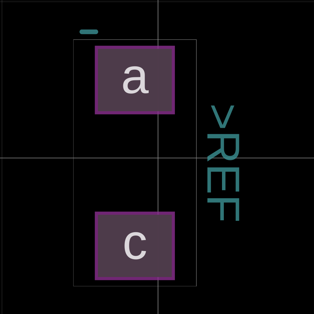
Through Hole Land Patterns
Radial Through Hole Land Patterns
Supported two-pin through hole land patterns are either axial or radial.
public defn make-two-pin-radial-landpattern (component-diameter:Toleranced,
lead-spacing:Double,
lead-diameter:Toleranced)
Create a two-pin radial landpattern.
component-diameter: the diameter of the component packagelead-spacing: the distance between leads.lead-diameter: the diameter of the leads.
public defn make-two-pin-radial-landpattern (component-diameter:Toleranced,
lead-spacing:Double,
lead-diameter:Toleranced
polarized?:True|False)
Create a two-pin radial landpattern with optional polarity.
component-diameter: the diameter of the component packagelead-spacing: the distance between leads.lead-diameter: the diameter of the leads.polarized?:trueif the land pattern is polarized,falseotherwise.
Axial Through Hole Land Patterns
public defn make-two-pin-axial-landpattern (component-diameter:Toleranced,
lead-spacing:Double,
lead-diameter:Toleranced)
Create a two-pin radial landpattern.
component-diameter: the diameter of the component packagelead-spacing: the distance between leads.lead-diameter: the diameter of the leads.
public defn make-two-pin-axial-landpattern (component-diameter:Toleranced,
lead-spacing:Double,
lead-diameter:Toleranced
polarized?:True|False)
Create a two-pin radial landpattern with optional polarity.
component-diameter: the diameter of the component packagelead-spacing: the distance between leads.lead-diameter: the diameter of the leads.polarized?:trueif the land pattern is polarized,falseotherwise.
Small Outline Land Patterns
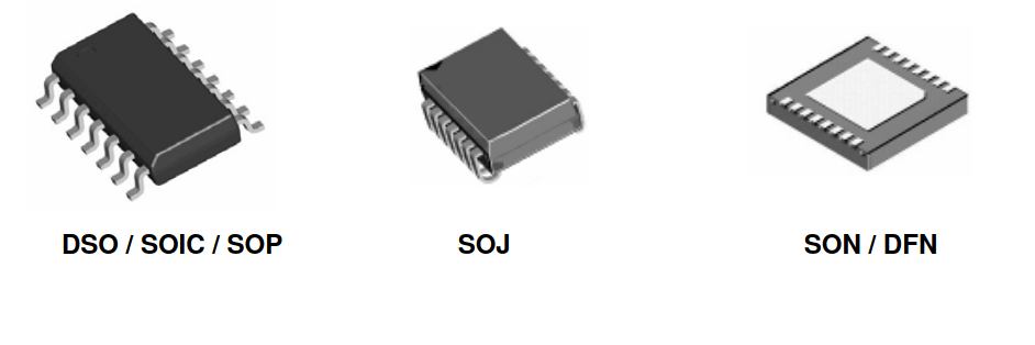
A small outline (SO) package is a package with pins along two sides of the component.
JEDEC symbol to JITX Generator Arguments
The following table may help in converting JEDEC-style dimensions into arguments for the JITX small outline landpattern generator.
| JEDEC Symbol | JITX Argument |
|---|---|
| b | terminal-width |
| D | package-length |
| E | lead-span |
| E1 | package-width |
| e | pitch |
| L | terminal-length |
| n | num-pins |
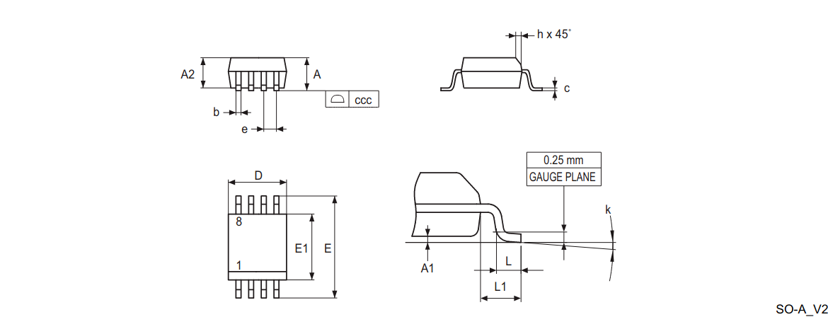
public defn make-n-pin-soic-landpattern (num-pins:Int,
pitch:Double, ; e
lead-span:Toleranced, ; E
package-length:Toleranced, ; E1
package-width:Toleranced, ; D
terminal-length:Toleranced, ; L
terminal-width:Toleranced) ; b
Create an SO land pattern.
num-pins: the number of pins of the package (must be even).pitch: the pitch of the leads or terminals (mm),ein the table above.lead-span: the distance from lead-edge to lead-edge (mm),Ein the table above.package-length: the size of the package in the same dimension as thelead-span(mm),E1in the table above.package-width: the size of the package in the orthogonal dimension aslead-span(mm),Din the table above.terminal-length: the length of terminals or leads in contact with the land pattern (mm),Lin the table above.terminal-width: the size of the terminals or leads in contact with the land pattern, in the orthogonal dimension toterminal-length(mm),bin the table above.
Example Usage
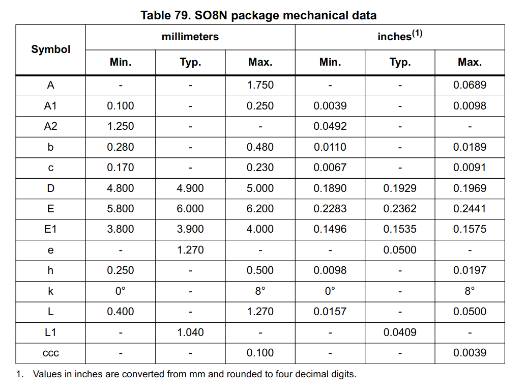
pcb-landpattern SO8N :
make-n-pin-soic-landpattern(8, ; number of pins
1.27 ; pitch
min-typ-max(5.8, 6.0, 6.2) ; lead-span
min-typ-max(4.8, 4.9, 5.0) ; package-length
min-typ-max(3.8, 3.9, 4.0) ; package-width
min-typ-max(0.4, 0.8, 1.27) ; lead-length, using average as typical
min-typ-max(0.28, 0.38, 0.48)) ; lead-width, using average as typical
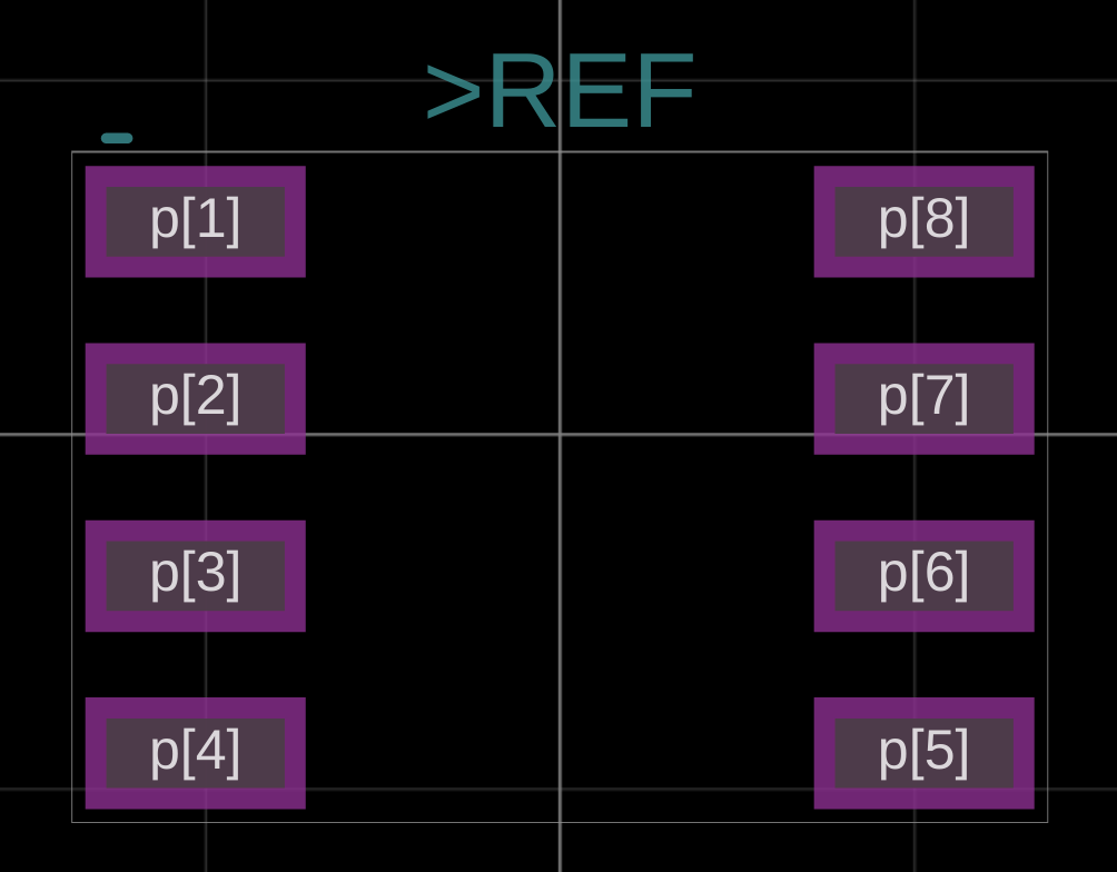
See The Model a Land Pattern tutorial for more details on parametric land pattern generation.
SOT Land Patterns
SOT landpatterns can be defined using the more general purpose API call, make-dual-row-smd-landpattern which creates a two-row SMD land pattern with different numbers of pins on either side.
public defn make-dual-row-smd-landpattern (primary-num-pins: Int,
secondary-num-pins: Int,
primary-pin-pitch: Double,
secondary-pin-pitch: Double,
lead-span: Toleranced,
package-length: Toleranced,
package-width: Toleranced,
terminal-length: Toleranced,
terminal-width: Toleranced,
polarity-marker?: True|False)
primary-num-pins: the number of pins on one side of the land patternsecondary-num-pins: the number of pins on the other side of the land patternprimary-pin-pitch: the pitch of pins on the primary side of the land patternsecondary-pin-pitch: the pitch of the pins on the other side of the land patternlead-span: the lead span across the land patternpackage-length: the length of the packagepackage-width: the width of the packageterminal-length: the length of the terminalsterminal-width: the width of the terminalspolarity-marker?: whether to add a polarity marker to the landpattern or not
Example Usage
pcb-landpattern SOT-23 :
make-dual-row-smd-landpattern(
n1, n2, p1, p2,
lead-span, package-length, package-width,
terminal-length, terminal-width,
polarity-marker?: True|False) where :
val n1 = 2
val n2 = 1
val p1 = 1.9
val p2 = 0.0 ; unneeded for one pin
val lead-span = min-typ-max(2.1, 2.37, 2.634) ; E
val package-length = tol(1.3, 0.1) ; E1
val package-width = min-typ-max(2.8, 2.9, 3.04), ; D
val terminal-length = tol(0.4, 0.1)
val terminal-width = tol(0.5, 0.1)
val polarity-marker? = false
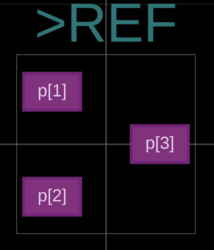
QFP Land Patterns
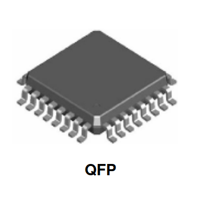
A quad flat package (QFP) is a package with pins along all four sides of the component.
JEDEC symbol to JITX Generator Arguments
| JEDEC Symbol | JITX Argument |
|---|---|
| b | terminal-width |
| D, E | lead-span |
| E1, D1 | package-size |
| e | pitch |
| L | terminal-length |
| n | num-pins |
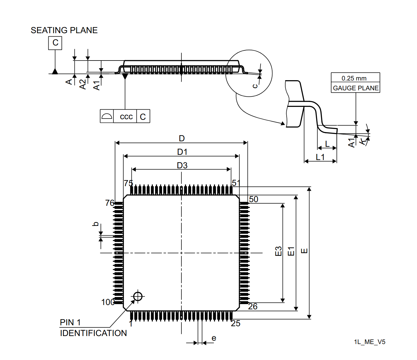
public defn make-qfp-landpattern (num-pins:Int,
pitch:Double, ; e
lead-span:Toleranced, ; E, D
package-size:Toleranced, ; E1, D1
terminal-length:Toleranced, ; L
terminal-width:Toleranced ; b
exposed-metal-heat-feature?:Shape ; optional thermal pad
num-pins: the number of pins of the package (must be even).pitch: the pitch of the leads or terminals (mm),ein the table above.lead-span: the distance from lead-edge to lead-edge (mm),Ein the table above.package-size: the size of the package,E1, D1in the table above. The package is assumed to be square.terminal-length: the length of terminals or leads in contact with the land pattern (mm),Lin the table above.terminal-width: the size of the terminals or leads in contact with the land pattern, in the orthogonal dimension toterminal-length(mm),bin the table above.exposed-metal-heat-feature?: an optional parameter for a thermal pad shape.
Example Usage
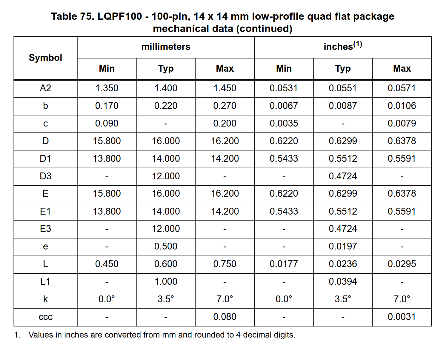
pcb-landpattern QFP-100 :
make-qfp-landpattern(
num-pins, pitch,
lead-span, package-size,
terminal-length, terminal-width,
thermal-pad) where :
val num-pins = 100 ; the total number of pins
val pitch = 0.5 ; the distance between pin centers
val lead-span = min-typ-max(15.8, 16.0, 16.2) ; the distance between the outer edges of the leads
val package-size = min-typ-max(13.8, 14.0, 14.2) ; the size of the package, assumed to be square
val terminal-width = min-typ-max(0.17, 0.22, 0.27) ; the width of the leads
val terminal-length = min-typ-max(0.45, 0.60, 0.70) ; the length of the leads
val thermal-pad = false
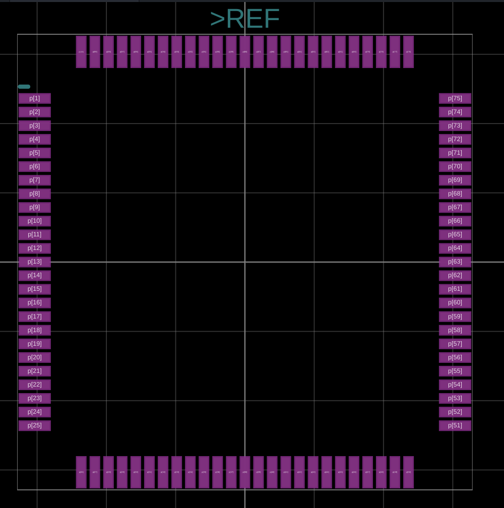
QFN Land Patterns
A quad flat package no-lead (QFN) is a quad landpattern where the terminals are pads on the underside of the component, as opposed to leads that extend outside the component (see QFP Land Patterns).
JEDEC symbol to JITX Generator Arguments
| JEDEC Symbol | JITX Argument |
|---|---|
| b | terminal-width |
| E, D | package-size |
| e | pitch |
| L | terminal-length |
| n | num-pins |
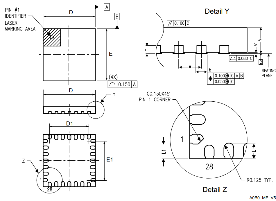
public defn make-qfn-landpattern (num-pins:Int,
pitch:Double, ; e
package-size:Toleranced, ; E, D
terminal-length:Toleranced, ; L
terminal-width:Toleranced, ; b
corner-pads?:False|[Pad, Pad], ; L1 x b
exposed-metal-heat-feature?:Shape|False) : ; optional thermal pad
num-pins: the number of pins of the package (must be even).pitch: the pitch of the leads or terminals (mm),ein the table above.package-size: the size of the package,E,Din the table above. The package is assumed to be square.terminal-length: the length of terminals or leads in contact with the land pattern (mm),Lin the table above.terminal-width: the size of the terminals or leads in contact with the land pattern, in the orthogonal dimension toterminal-length(mm),bin the table above.corner-pads?: optional pair ofpcb-paddefinitions to use to replace the corner pads on the landpattern.exposed-metal-heat-feature?, an optional
Example Usage
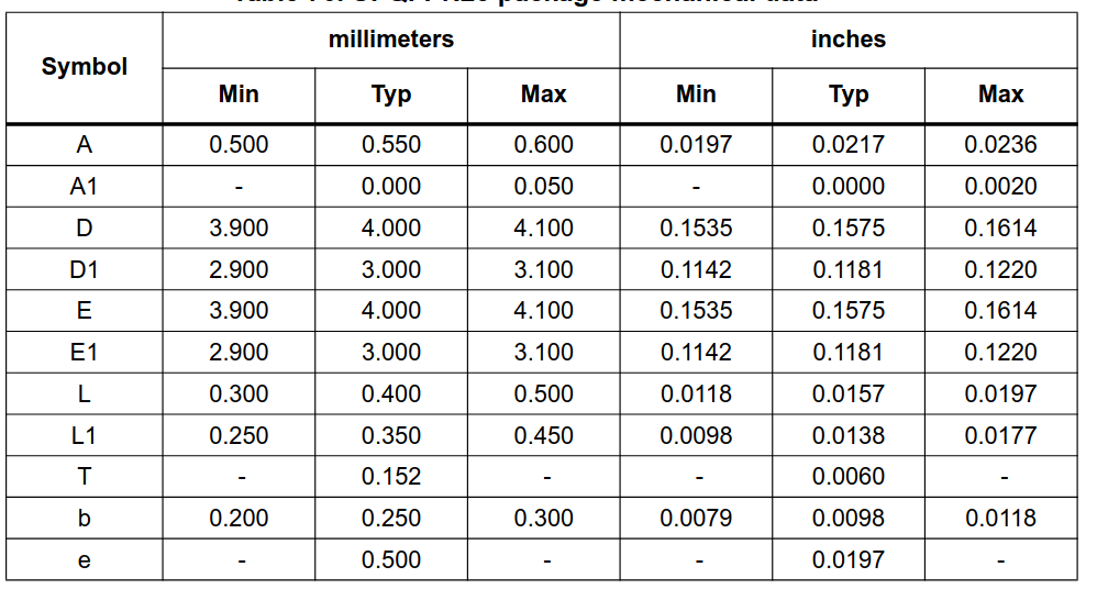
pcb-landpattern QFN-28 :
make-qfn-landpattern(
num-pins, pitch,
package-size, lead-length, lead-width
corner-pads,
thermal-pad,) where :
val num-pins = 28 ; the total number of pins, must be divisible by 4
val pitch = 0.5 ; the pitch of the pins
val package-size = min-typ-max(3.90, 4.00, 4.10) ; the size of the package, assumed to be square
val lead-length = min-typ-max(0.30, 0.40, 0.50) ; the length of the lead terminals
val lead-width = min-typ-max(0.20, 0.25, 0.30) ; the width of the lead terminals
; Optional Corner Pad Modifiers
val corner-pads = [
smd-pad(loc(-0.1, 0.0) * Rectangle(0.45, 0.21))
smd-pad(loc(-0.1, 0.0) * Rectangle(0.45, 0.21))
]
; Optional thermal pad
val thermal-pad = false
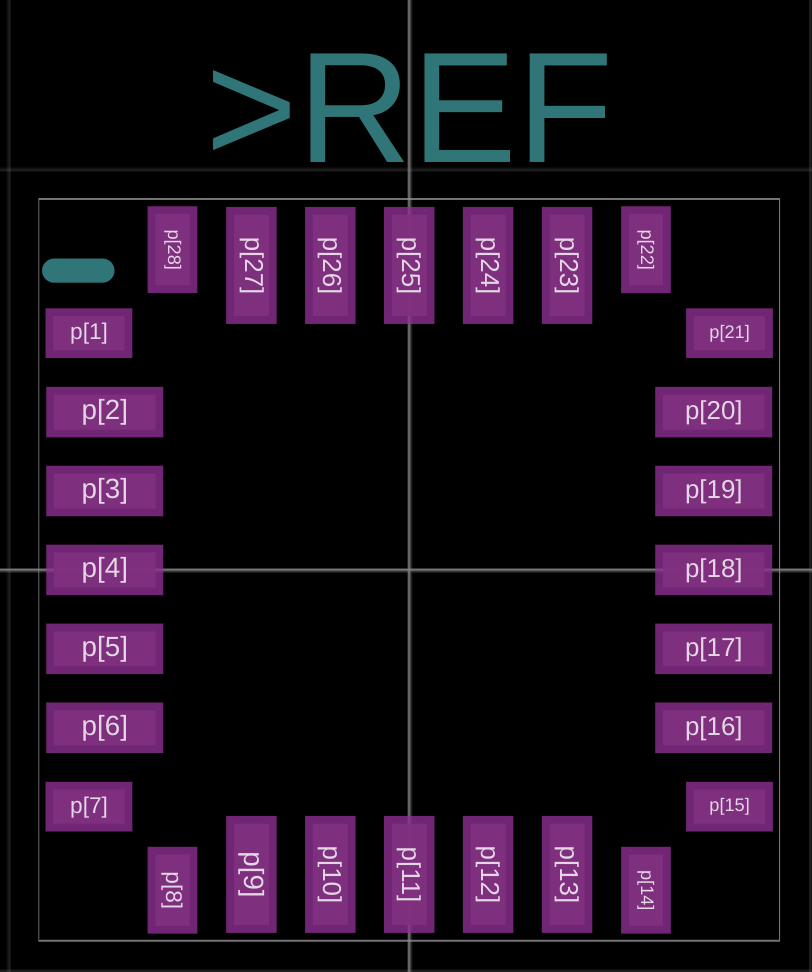
Note: some trial and error might be required to find dimensions for corner pad overrides. In this case, the length was found using the
maxvalue of L1 in the table, and the width was found empirically by measuring the width of the other pads.
BGA Land Patterns
A ball grid array (BGA) package uses a matrix of solder balls on the bottom of the package, as opposed to exposed metal terminals.
JEDEC symbol to JITX Generator Arguments
| JEDEC Symbol | JITX Argument |
|---|---|
num-rows | |
num-cols | |
| b | ball-diameter |
| D | package-width |
| E | package-length |
| e | pitch |
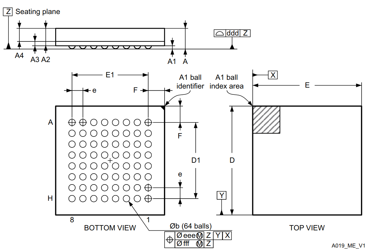
num-cols:Int,
pitch:Double,
ball-diameter:Double,
package-length:Toleranced,
package-width:Toleranced,
modifier:BGAModifier) :
num-rows: the number of rows of packagenum-cols: the number of columns of the packagepitch: the pitch of the solder bumpsball-diameter: the nominal/typical diameter of the solder ballspackage-length: the length of the packagepackage-width: the width of the packagemodifier: the depopulation and/or pitch modifier
Example Usage
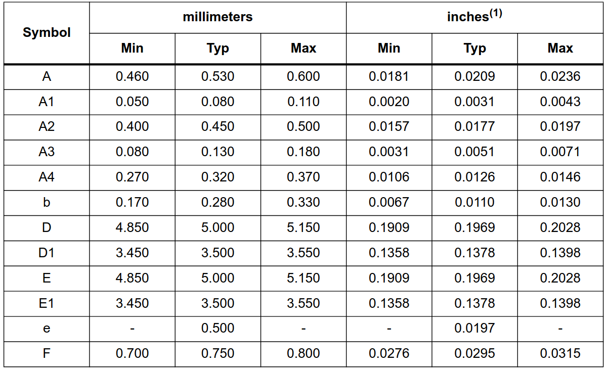
pcb-landpattern BGA-64 :
make-bga-landpattern(
num-rows, num-cols
pitch, ball-diameter
package-length, package-width
modifier
) where :
val num-rows = 8 ; Number of rows in the matrix
val num-cols = 8 ; Number of columns in the matrix
val pitch = 0.50 ; the spacing between ball centers
val ball-diameter = 0.28 ; the diameter of the solder balls
val package-length = min-typ-max(4.85, 5.0, 5.15) ; the length of the package
val package-width = min-typ-max(4.85, 5.0, 5.15) ; the width of the package
; The BGA Modifier. See ocdb/utils/landpatterns for more
; modifiers, supported are StaggeredMatrix, EquilateralTriangleMatrix,
; PerimeterMatrix, ThermallyEnhancedMatrix.
val modifier = FullMatrix()
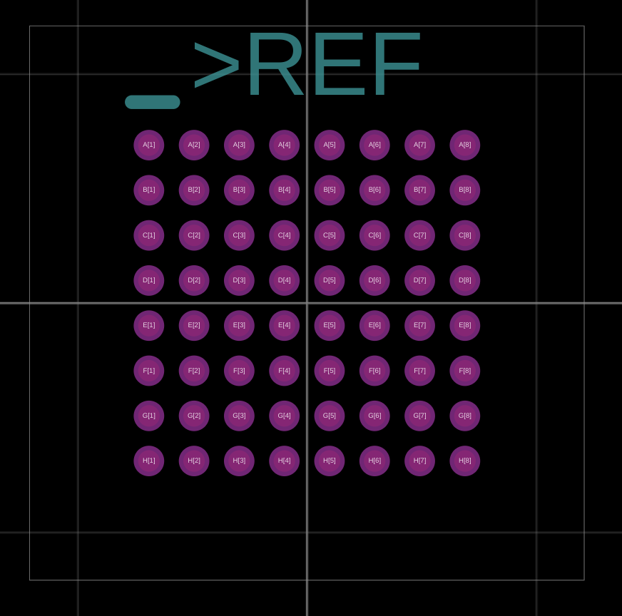
Depopulation Modifiers
The make-bga-package argument uses a special argument named modifier which allows for a variety of depopulation and ball spacing strategies. The currently supported depopulation modifiers are:
FullMatrix
In a FullMatrix (the default) no pads will be depopulated.
defn FullMatrix () -> BGAModifier
StaggeredMatrix
In a StaggeredMatrix, every other pad is depopulated.
defn StaggeredMatrix () -> BGAModifer
PerimeterMatrix
In a PerimeterMatrix, a range of rows and columns in the center will be depopulated
defn PerimeterMatrix (rows:Range, cols:Range) -> BGAModifer
rows: the range of rows to depopulatecols: the range of cols to depopulate
Usage :
; rows 3,4,6 and columns 4,5 will be depopulated.
val modifier = PerimeterMatrix(3 through 6, 4 through 5)
ThermallyEnhancedMatrix
A ThermallyEnhancedMatrix is like a PerimeterMatrix, except with some region in the center remaining populated.
defn ThermallyEnhancedMatrix (perimeter-rows:Range, perimeter-cols:Range
interior-rows:Range, interior-cols:Range ) -> BGAModifer
perimeter-rows: the range of rows to depopulateperimeter-cols: the range of columns to depopulateinterior-rows: the range of rows in the center to remain populatedinterior-cols: the range of columns in the center to remain populated
Usage :
; Pins (5,5) through (6,6) will be populated, while the other
; pins within the range (4,4) through (7,7) will be depopulated.
val modifier = ThermallyEnhancedMatrix(
4 through 7, 4 through 7,
5 through 6, 5 through 6,
))
EquilateralTriangleMatrix
An "EquilaterTriangleMatrix" is like a staggered matrix, but where the pads are all equistance from eachother. This means for any three adjacent pads with two in the same row or column, the centers of the pads form an equilateral triangle.
defn EquilateralTriangleMatrix () -> BGAModifier
CustomDepop
The CustomDepop modifier allows the caller to specify which pins are depopulated using a callback.
defn CustomDepop (callback: (Int, Int) -> True|False)
Usage :
defn depop? (row:Int, col:Int) :
; Specify a list of custom depopulated pins
val depopulated = [
[0, 2]
[0, 5]
[2, 8]
[3, 0]
[5, 8]
[6, 0]
[8, 3]
[8, 6]
]
contains?(depopulated, [row, col])
val modifier = CustomDepop(depop?)
ocdb/utils/land-protrusions
ocdb/utils/land-protrusions is a set of lookup tables used to satisfy IPC compliance during the generation of land patterns. It defines a set of LandProtrusionTypes that represent metadata about package leads or terminations that is used alongside DensityLevel in order to compute offsets to the pads and courtyards of land patterns.
Data Types
public pcb-enum ocdb/utils/land-protrusions/LandProtrusionType :
SmallFlatRibbonLLeads, ; Flat ribbon L leads for pitch less than 0.0625mm
SmallGullWingLeads, ; Gull wwing leads with pitch less than 0.0625mm
BigFlatRibbonLLeads, ; Flat ribbon L leads for pitch greater than 0.0625mm
BigGullWingLeads, ; GullWing leads for pitch greater than 0.0625mm
JLeads, ; J Leads
SmallRectangularLeads, ; Leads for rectangular components (chip capacitors, resistors, inductors) smaller than 0601
BigRectangularLeads, ; Leads for rectangular components (chip capacitors, resistors, inductors) 0601 or larger
CylindricalLeads, ; Cylindrical end cap leads
LeadlessChipCarrierLeads, ; Lead less chip carrier leads
ConcaveChipArrayLeads, ; Concave chip array leads
ConvexChipArrayLeads, ; Convex chip array leads
FlatChipArrayLeads, ; Flat chip array leads
ButtJointLeads, ; Butt joint leads
InwardFlatRibbonLLeads, ; Inward flat ribbons L leads
FlatLugLeads, ; flat lug leads
QuadFlatNoLeads, ; quad flat components without leads
SmallOutlineNoLeads, ; small outline packages without leads
SmallOutlineFlatLeads, ; small outline flat leads
ShortTwoPinCrystalLeads, ; two pin crystal components shorter than 10mm
ShortAluminumElectrolyticLeads, ; electrolytic capacitor shorter than 10mm
TallTwoPinCrystalLeads, ; two pin crystal components 10mm or taller
TallAluminumElectrolyticLeads, ; electrolytic capacitor 10mm or taller
LandProtrusionType is a helper enum for various kinds of leads and terminations on components. It is used to configure their generated land patterns.
public pcb-struct ocdb/utils/land-protrusions/LeadFillets:
toe:Double ; space away from the component towards the board
heel:Double ; space towards the component
side:Double ; space on the edges of the lead
courtyard-excess:Double ; additional area to add to the courtyard
LeadFillets is a helper struct that represents the space added to pads and courtyard area when generating land patterns.
Functions
public defn lead-fillets (lead-type:LandProtrusionType) -> LeadFillets
public defn lead-fillets (lead-type:LandProtrusionType, density-level:DensityLevel) -> LeadFfillets
A helper function to lookup the LeadFillets corresponding to a LandProtrusionType given a DensityLevel. If not supplied, the DensityLevel used is the default defined in Design Variables
public defn bga-courtyard-excess (density-level:DensityLevel) -> Double
A helper function to lookup the courtyard excess when computing BGA land patterns.
Properties
JITX allows us to associate arbitrary properties with pins, components, and modules. These properties are used throughout OCDB for design calculations and design review checks. Everyone is free to define and use their own parameters, but when we collaborate on a shared set it is easier to write better automation. What follows is documentation of the properties defined in OCDB.
Component properties
These are properties associated with components, including passive components like resistors, capacitors, and inductors.
Generic properties
These properties apply to all components.
| Name | Type | Values | Unit | Description |
|---|---|---|---|---|
temperature | Double | degC | Bulk temperature of the component | |
rated-temperature | Toleranced False | e.g. min-max() or false | degC | Rated operating temperature of component. Use false if property does not apply. |
trust | String | “low” | The data for this component came from a distributor/other | |
| “datasheet”, "medium" | The data from this component came from the datasheet | |||
| “built”, "high" | This component was used on a board without issue | |||
| “characterized” | The this model data was characterized in the lab | |||
dimensions | [Double, Double, Double] | [Length, Width, Height] | [mm, mm, mm] | Length, width and height (x,y,z) of the bounding box of the component |
mounting | String | “smd” “through-hole” | How is this component mounted to the board | |
case | String | “0402”, "0805" | Common name of the component package |
Resistor properties
These are properties associated with resistors, as used by gen-res-cmp in ocdb/utils/generic-components.
| Name | Type | Values | Unit | Description |
|---|---|---|---|---|
resistor | True|False | true | Identifies resistor component | |
type | String | “thick-film”, “metal-film”, ... | Type of resistor | |
resistance | Double | Ohm | Nominal resistance | |
tolerance | Double | Ohms/Ohm | Guaranteed tolerance from manufacturer | |
rated-voltage | Double | Volts | Maximum voltage rating from manufacturer | |
rated-power | Double|PWL[temp] | Watts|[degC, Watts] | Power dissipation limit as rated by manufacturer. One value, or set of points for PWL function. | |
derating | PWL[temp] | [degC, derate factor] | Temperature-based derating of resistance | |
TCR | Double | Ohms/Ohm*degC | Temperature coefficient of resistance |
Capacitor properties
These are properties associated with capacitors, as used by gen-cap-cmp in ocdb/utils/generic-components.
| Name | Type | Values | Unit | Description |
|---|---|---|---|---|
capacitor | True|False | true | Identifies capacitor component | |
type | String | “ceramic”, “film”, “electrolytic" | Type of capacitor | |
anode | String | “aluminum”, “tantalum”, “niobium-oxide” | Anode material of electrolytic capacitor | |
electrolyte | String | “polymer”, “manganese-dioxide”, “hybrid”, “non-solid” | Electrolyte material of electrolytic capacitor | |
temperature-coefficient | String | “X7R”,"X5R", "NP0", "C0G",... | Temperature coefficient of capacitance | |
capacitance | Double | Farad | Nominal capacitance | |
tolerance | Double | Farad/Farad | Guaranteed tolerance from manufacturer | |
rated-voltage | Double | Volts | Maximum voltage rating from manufacturer | |
rated-current-pk | Double | Amperes | Maximum peak current rating from manufacturer | |
rated-current-rms | Double|PWL[temp] | Amperes | Maximum rms current rating from manufacturer |
Inductor properties
These are properties associated with inductors, as used by gen-ind-cmp in ocdb/utils/generic-components.
| Name | Type | Values | Unit | Description |
|---|---|---|---|---|
inductor | True|False | true | Identifies component as inductor | |
type | String | “wirewound”, “Thick Film”, ... | Type of inductor | |
material-core | String | “ceramic”, “ferrite”, ... | Composition of inductor | |
inductance | Double | Henry | Nominal inductance | |
tolerance | Double | henry/henry | Guaranteed tolerance from manufacturer | |
current-rating | Double | Amperes | Maximum steady-state current rating from manufacturer | |
saturation-current | Double | Amperes | Percentage inductance drop (typ 20-30%) at peak currents | |
shielding | String | “semi-shielded”, “shielded”, “unshielded” | Magnetic field status | |
dc-resistance | Double | ohm | Nominal resistance | |
quality-factor | Double | ratio@freq | Loss factor inverse - ratio between inductors resistance and inductance | |
self-resonant-frequency | Double | Hertz | Frequency at which inductor impedance becomes very high / open circuit |
Crystal properties
These are properties associated with crystals, as used by gen-xtal-cmp in ocdb/utils/generic-components.
| Name | Type | Values | Unit | Description |
|---|---|---|---|---|
crystal-resonator | CrystalResonator() | see below | Collection of properties for a resonator |
public pcb-struct ocdb/utils/property-structs/CrystalResonator :
load-capacitance:Double ; Load capacitance in Farads
shunt-capacitance:Double ; Shunt capacitance in Farads
motional-capacitance:Double ; Motional capacitance in Farads
ESR:Double ; Series resistance of crystal in Ohms
frequency:Double ; Fundamental frequency in Hz
frequency-tolerance:Double ; Frequency tolerance in Hz
max-drive-level:Double ; Max drive level in W
; Example call
property(self.crystal-resonator) = ocdb/utils/property-structs/CrystalResonator(cl, cs, cm, esr, f, df * f, dl)
Pin properties
These properties are associated with component pins like power, reset, and logic pins.
Power pins
| Name | Type | Values | Unit | Description |
|---|---|---|---|---|
power-pin | PowerPin(Toleranced) | e.g. min-max() or min-typ-max() | Volts | Power pin definition using the structure PowerPin() taking a Toleranced argument for the allowable voltage range |
supply-pin | PowerSupplyPin(Toleranced, Double) | Volts|[Volts,Amps] | Nominal voltage and optional current capacity of the power pin | |
gnd-ref | pin or net object | JITXObject | Identifier for a pin or net that is the 0v reference for this pin | |
power-request | [Double,Double,Double] | [Voltage, Current, Noise] | [Volts, Amperes, Volts] | Defines a load by nominal voltage, current, and allowable noise to be satisfied by the power solver. |
Logic pins
Digital pins
These are properties to check the generic rated voltage and ESD protection of pins, used by the checks in ocdb/utils/checks.
| Name | Type | Values | Unit | Description |
|:-----|:-----|:-------|:-----|:------------|
| generic-pin | GenericPin() | see below | | Properties for rated voltage and ESD protection. |
; Library property name: generic-pin
public pcb-struct ocdb/utils/property-structs/GenericPin :
max-voltage:Toleranced|RelativeVoltage ; Maximum voltage that can be applied to pin (V)
rated-esd:Double ; Rated ESD voltage (V)
; Example call
property(self.SDA.generic-pin) = GenericPin(min-max(-0.3, 3.6), 1500.0)
| Name | Type | Values | Unit | Description |
|---|---|---|---|---|
digital-input | DigitalInput() | see below | Properties to check digital inputs |
; Library property name: digital-input
public pcb-struct ocdb/utils/property-structs/DigitalInput :
vil:Toleranced|RelativeVoltage ; Range of voltages that will read as logic low (V)
vih:Toleranced|RelativeVoltage ; Range of voltages that will read as logic high (V)
vdd-pin:JITXObject ; Pin that powers the high reference
gnd-pin:JITXObject ; Pin that powers the low reference
leakage-current:Double ; Leakage current in Amps
; Example call
property(UART-RX.digital-input) = DigitalInput(0.4, 0.7 * vcc, VCCIO, GND, 1.0e-6)
| Name | Type | Values | Unit | Description |
|---|---|---|---|---|
digital-output | DigitalOutput() | see below | Properties to check digital inputs |
; Library property name: digital-output
public pcb-struct ocdb/utils/property-structs/DigitalOutput :
driver:LogicFamily ; Driver model of the output
tristateable:True|False ; Can this pin be put in a high-impedance mode?
vdd-pin:JITXObject ; Pin that powers the high reference
gnd-pin:JITXObject ; Pin that powers the low reference
; Example Call
property(UART-TX.digital-output) = DigitalOutput(CMOSOutput(min-max(0.3, 0.5), min-max(2.6, 3.3)), false, VCCIO, GND)
| Name | Type | Values | Unit | Description |
|---|---|---|---|---|
digital-io | DigitalIO() | see below | Properties to check digital io pins |
; Library property name: digital-io
public pcb-struct ocdb/utils/property-structs/DigitalIO :
driver:LogicFamily ; Driver model of the output
vil:Toleranced|RelativeVoltage ; Range of voltages that will read as logic low (V)
vih:Toleranced|RelativeVoltage ; Range of voltages that will read as logic high (V) gnd-pin:JITXObject ; Pin that powers the driver low reference
vdd-pin:JITXObject ; Pin that powers the high reference
gnd-pin:JITXObject ; Pin that powers the low reference
leakage-current:Double ; Leakage current in Amps
; Example call
property(PA[3].digital-io) = DigitalIO(CMOSOutput(min-max(0.0, 0.4), min-max(3.3 - 0.4, 3.3)), typ(0.3 * 3.3), typ(0.7 * 3.3), self.VDD, self.VSS, 50.0e-9)
Closest Standard Value
How to find the closest standard value for a resistor, capacitor, or inductor.
If you've computed the value you need for a resistor, capacitor, or inductor, and now you need to compute the closest normal value to that computed value, you can use closest-std-val.
closest-std-val
closest-std-val take a value and a tolerance as input, and return a standard/normal/nominal EIA value you can use to create or query your basic components (resistor, capacitor, or inductor):
; Returns the closest value to v in the tolerance range specified by tol
public defn closest-std-val (v:Double, tol:Double)
Example usage:
; get the required resistance, given the input voltage and the desired current
val computed-resistance = (voltage - typ(vf)) / typ(computed-current)
; turn the resistor into the closest standard value resistor by passing in a the resistance that we computed
val standard-computed-resistance = closest-std-val(typ-value(computed-resistance), 5.0)
Adding Mounting Holes
JITX contains utilities to add mounting holes to a board automatically. A single call to add-mounting-holes can add a mounting hole to each corner of your board.
In order to add mounting holes to your board, call add-mounting-holes with your board shape, the size of screw that you want, and optionally a Tuple which specifies the corners that you don't want holes added:
; Add mounting holes to the board given its shape, a screw size, and hole indices to exclude.
public defn add-mounting-holes (board-shape:Shape, screw-size:String|Double, no-hole:Tuple<Int>)
If you want holes added to every corner of the board:
; Add mounting holes to the board given its shape and a screw size.
public defn add-mounting-holes (board:Shape, screw-size:String|Double):
add-mounting-holes(board, screw-size, [])
Other mounting hole utilities also exist:
; Add mounting holes to the board given its shape. Defaults to M3 size holes.
public defn add-mounting-holes (board:Shape)
; Add mounting holes to the board given its shape, excluding holes given
; by the indices in no-holes. Defaults to M3 size mounting holes.
public defn add-mounting-holes (board:Shape, no-hole:Tuple<Int>)
Screw Sizes
The screw size is specified by a string, and can be any one of the following:
- "M2"
- "M2p5"
- "M3"
- "M3p5"
Testpoint - how to place a testpoint
We can place a testpoint for any net with a call to testpoint-strap.
Here is the built-in definition of testpoint-strap:
; place a testpoint
defn testpoint-strap (tp:JITXObject, tp-name:String, diameter:Double) -> JITXObject:
It accepts a net to place the testpoint for, a name to apply to the testpoint, and the diameter you want the circular SMD test pad to be.
Example Usage
; add a testpoint for this pin
val test-pad = my-testpoint-strap(IN, net-name, 2.0) ; in current versions of OCDB, we can directly call `testpoint-strap` function
Make-Net
make-net is another way to create connection between components. It creates the exact same type of connection that the net statement makes.
However, make-net allows us to name nets with strings. This tends to be useful when constructing nets inside for loops or in recursive functions.
Signature
defn make-net (name:Symbol, refs:Seqable<JITXObject>) :
...
defn make-net (name:Symbol, type:PortType|False, refs:Seqable<JITXObject>) :
...
defn make-net (name:Symbol, type:PortType|False, refs:Seqable<JITXObject>, public?:True|False) :
...
name- Name as aSymbolfor this nettype- Constructs a net of a particular port type likeSinglePin,Bundle, orPortArray.FalseimpliesSinglePinrefs- Object capable of generating a sequence ofJITXObjects like ports or nets - same list of refs you would pass to thenetstatement.public?- Flag to make this net publicly accessible outside the module. By default this value isfalse.
Example usage
pcb-module top-level:
inst host : mcu
inst sensor : temp-sensor
val name = to-string("alert-%_" % [1])
val symb = to-symbol(name)
make-net(symb, [host.GPIO[0], sensor.ALERT])
In this example, we connect a GPIO pin on the host to the ALERT output of a sensor using the make-net function. This is a contrived example and only intended to show
the mechanics of the make-net function.
Symbols - set symbols of a net
We can set any net to use a specified symbol. This is especially useful for power and gnd nets.
You can design your own symbol, or you can use any of the many built-in symbols.
Example
To assign power symbols to the GND and POWER nets, we could specify the following in our top level pcb-module:
; set symbols of some nets
symbol(GND) = ocdb/utils/symbols/ground-sym
symbol(POWER) = ocdb/utils/symbols/supply-sym
LayerIndex
The LayerIndex type is used to specify which conductor layer in the board stackup that a particular statement or property affects.
Outline
defstruct LayerIndex :
index:Int
side:Side
defn LayerIndex (index:Int, side:Side = Top) -> LayerIndex:
...
The LayerIndex type expects two arguments:
index- If we consider the conductor layers in board stackup an zero-indexed array, theindexis the offset into the array from either theTopor theBottom.side- This parameter determines whether theindexapplies from theTopgoing down, or from theBottomgoing up.
Symmetry of Top and Bottom Indices
The Bottom side indices can be considered a reverse indexing scheme.
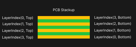
Notice that there is a way to index every layer in the stackup in either direction.
Shortcuts based on Side
In some applications of the LayerIndex type, you will often see the type LayerIndex|Side used. This means that the user can pass either a LayerIndex or a Side parameter in the form of Top or Bottom enumerated values.
These Side values are a shortcut for:
Top=>LayerIndex(0, Top)Bottom=>LayerIndex(0, Bottom)
Operators
Currently the plus and minus operators are defined for the LayerIndex and Side types. This provides a short cut for indexing:
val inner-1 = Top + 1
println("Inner 1: %_" % [inner-1])
val inner-N-1 = Bottom - 1
println("Inner N-1: %_" % [inner-N-1])
val inner-skip = inner-1 + 2
println("Inner Skip: %_" % [inner-skip])
When run this will generate:
Inner 1: LayerIndex(1)
Inner N-1: LayerIndex(1, Bottom)
Inner Skip: LayerIndex(3)
LayerSpecifier
The LayerSpecifier type is the base type for identifying non-copper manufacturing layers. This typically includes the silkscreen, solder mask, forbidden regions, etc. It does not include the copper layers. To identify copper layers, we use the LayerIndex type.
Derived Types
LayerSpecifier is the parent to multiple child types. The child types defined below are what we typically use with the layer() statement.
| Name | Description |
|---|---|
Courtyard(s:Side) | Courtyard layer to indicate land pattern bounds. Expects a Top|Bottom argument. |
Cutout() | Cutout layer for holes and slots. Vias and through-hole pads will include their hole definitions on this layer. |
SolderMask(s:Side) | Solder mask layer. Expects a Top|Bottom argument. |
Paste(s:Side) | Paste application layer. Expects a Top|Bottom argument. |
Glue(s:Side) | Glue application layer. Expects a Top|Bottom argument. |
Finish(s:Side) | Surface Finish layer to indicate plating. Expects a Top|Bottom argument. |
Silkscreen(<br>  name:String,<br>  s:Side<br>) | Silkscreen application layer. Expects a string name and a Top|Bottom argument. |
BoardEdge() | Geometry to align with edge of board |
ForbidVia() | Forbid Vias layer (via keepout) |
ForbidCopper(<br>  start:LayerIndex,<br>  end:LayerIndex<br>) | Forbid Copper layer (copper keepout). Expects a LayerIndex argument to specify which layer[s] to forbid copper. |
CustomLayer(<br>  name:String,<br>  s:Side<br>) | Custom Mechanical layer. Expects a name and a Top|Bottom argument. |
Cutout
The Cutout layer is intended to make internal holes in the board shape, like for through holes or routed holes/slots.
While you can use any geometry on the Cutout layer - keep in mind your fabricator's limitations and constraints. If your fabricator only has a router (and not a laser or waterjet cutter) then they will likely not be able to construct a hole with squared corners.
Silkscreen
This layer expects a name:String argument. This name acts like a class attribute in HTML. It is intended to group like content together.
When the board data is exported, the silkscreen content for the top and bottom layers, respectively, will be flattened into a single top and bottom silkscreen layer.
CustomLayer
Similarly, the CustomLayer specifier expects a name:String argument. This argument allows the user to specify different classes of content like:
- Fabrication Notes
- Assembly Notes
- Dimensions
See the following links for how these layers map to export backends:
ForbidCopper
The ForbidCopper specifier takes a LayerIndex instance[s] as an argument. This allows you to construct keepout regions for the copper on any layer or set of layers in a design.
defn ForbidCopper (start:LayerIndex, end:LayerIndex = start) -> ForbidCopper :
...
Notice that the end by default is start. If you construct a ForbidCopper() with a single argument, then only that copper layer will possess a forbidden region.
Let's consider a case where we have an antenna on a N-layer board:
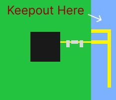
And we want to place a forbid region in the blue area of the board.
pcb-board curr-board:
...
val forbid-range = ForbidCopper(
LayerIndex(1), LayerIndex(0, Bottom)
)
layer(forbid-range) = loc(40.0, 0.0) * Rectangle(10.0, 30.0)
Here we construct a ForbidCopper instance that spans the layer 1 to N. Notice that we don't include the layer 0 or the Top layer because that is where the antenna structure will go. The LayerIndex(0, Bottom) is a means of specifying the bottom copper layer of the board without knowing the full number of layers in the stackup.
We then use the loc() function to position the desired forbid region on the board. This takes our 10mm x 30mm forbid region and translates it 40mm to right from the origin of the board.
Components
Sections
High Level Part Query
We can query actual parts from the JITX database that can be bought. Our database contains resistors, inductors, capacitors and STM micro-controllers.
Check the properties reference for a description of supported attributes.
Read about the Low Level Part Query API to learn about the syntax of the query requirements.
The high level functions in ocdb/utils/generic-components such as chip-resistor make calls to less specialized functions
in ocdb/utils/parts such as Resistor that make calls to the low level API such as dbquery-first.
Supported parameters
The supported special query parameters are:
- _exist : List of attributes that the returned documents must contain.
- _sort : The returned documents will be sort according to the list of attributes specified
by this parameter, applied in the order they appear. Sorting in descending fashion can
be obtained by starting a sorting attribute by a minus sign "−". This can take 2 additional value besides
the list of existing properties:
areais an alias fordimensions.areaandcostis an alias forprice.
Regular filter properties:
- We can filter on a part attribute :
{"category": "resistor"}. - For filtering over capacitance, resistance and inductance, those constraints are replaced by interval allowing for queries with a precision of 0.0005Ω, 0.01A and 0.01F respectively.
- For filtering over the tolerance :
{"tolerance": 0.05}will constrain the actual tolerance range to be included in the interval[-5%, 5%]. Returns 500 Bas Request if this is not a positive double - We can filter on a nested parameter using
.:{"dimensions.x": 11} - We can filter on a list of values giving a list :
{"case": ["Axial", "0402"]} - We can filter with an inequality prepending
min-ormax-:{"max−rated-power": 0.05}.max-x,max-yandmax-zare shorthands formax-dimensions.x,max-dimensions.y,max-dimensions.z - We interpret
minimum_quantityas a floor on bulk purchase size; we automatically convertminimum_quantitytomax-minimum_quantity.
Example:
#use-added-syntax(jitx)
defpackage my-design :
import ocdb/utils/generic-components
pcb-module my-module :
inst res : chip-resistor(["max-z" => 0.5, "_sort" => ["-rated-power"], "_exist" => ["tolerance"]])
Resistors
This sections details how to search and specify resistors in a design. There are over 1,000,000 resistors in the JITX database and the same part can be referenced in different packaging (cut tape, reels...).
chip-resistor finds a specific resistor based on specified properties and stock.
look-up-chip-resistors is a function that returns lists of resistors based on properties and stock.
res-strap does everything chip-resistor does and connects it to two nets.
gen-res-cmp allows us to place generic resistor components for offline use.
The db-parts section describes lower level functions, and the properties section describes every available attribute we can search with.
Contents:
- ocdb/utils/generic-components
- ocdb/utils/db-parts
- Properties
- Attribute:
resistance - Attribute:
tolerance (min, max) - Attribute:
manufacturer - Attribute:
mounting - Attribute:
case - Attribute:
type - Attribute:
composition - Attribute:
rated-power - Attribute:
tcr (neg, pos) - Attribute:
rated-temperature (min, max) - Attribute:
mpn - Attribute:
dimensions (x, y, z, area) - Attribute:
stock - Attribute:
price - Attribute:
minimum_quantity - Attribute:
metadata.datasheets - Attribute:
metadata.image - Attribute:
metadata.digi-key-part-number - Attribute:
metadata.description - Attribute:
metadata.series - Attribute:
metadata.packaging - Attribute:
metadata.features - Attribute:
metadata.supplier-device-package - Attribute:
metadata.number-of-terminations
- Attribute:
ocdb/utils/generic-components
The resistor functions are located in ocdb/utils/generic-components, which imports ocdb/utils/db-parts.
chip-resistor
We can query an actual SMD resistor from the JITX database that can be bought. This call requires internet access.
chip-resistor calls the lower level Part Query API adding the list of attributes provided
by the user on top of design settings.
public defn chip-resistor (params:Tuple<KeyValue>)
Here are the quick accessors:
public defn chip-resistor (resistance:Double)
public defn chip-resistor (resistance:Double, tolerance:Double)
The resistance is in Ohms and the tolerance is unit-less (0.01 is ±1%).
Example:
- res1 = 10 kΩ
- res2 = 0.01 Ω, 0.5% tolerance
- res3 = 0.01 Ω, 0.5% tolerance, 0.5 Watt or more
- res4 = 1 Ω, 0.5% tolerance, 1206 size
- res5 = 100 mΩ, 0.5% tolerance, 1210 size or larger
- res6 = 100 mΩ, 0.5% tolerance, 1210 size or larger, rated to 60° C or above
- res7 = First, the value is calculated ( (5-3)/0.005 = 400 Ω), then it's rounded to the closest 5% resistor value (402 Ω), then a 402 Ω resistor of 1% tolerance is returned.
#use-added-syntax(jitx)
defpackage my-design :
import ocdb/utils/generic-components
import ocdb/utils/design-vars
; Overrides default value set in ocdb/utils/design-vars
MIN-PKG = "0402"
pcb-module my-module :
inst res1 : chip-resistor(10.0e3)
inst res2 : chip-resistor(0.01, 0.005)
inst res3 : chip-resistor(["resistance" => 0.01 "tolerance" => 0.005 "min-rated-power" => 0.5])
inst res4 : chip-resistor(["resistance" => 1.0 "tolerance" => 0.005 "case" => "1206"])
inst res5 : chip-resistor(["resistance" => 100.0e-3 "tolerance" => 0.005 "case" => get-valid-pkg-list("1210")])
inst res6 : chip-resistor(["resistance" => 0.1 "tolerance" => 0.005 "case" => get-valid-pkg-list("1210") "min-rated-temperature.max" => 60.0])
var some-voltage = 3.0
val some-current = 5.0e-3
inst res7 : chip-resistor(closest-std-val( (5.0 - some-voltage) / some-current,0.5), 0.01)
Fixed Requirements :
- category: "resistor"
- mounting: "smd"
- minimum_quantity: 1
Default design Requirements (set by global variables defined in ocdb/utils/design-vars) :
- min-stock: 500
- _sort: ["area"]
- max-rated-temperature.min: 0.0
- min-rated-temperature.max: 25.0
- case: ["0201" "02016" "0202" "0302" "0303" "0402" "0404" "0503" "0505" "0603" "0612" "0805" "1206" "1210" "1218" "1812" "2010" "2512" "2525" "2615" "2616" "3920" "4122" "4823" "5329" "6030"]
Those design requirements can be changed, either by changing ocdb/utils/design-vars or by importing ocdb/utils/design-vars and
setting new values for the global variables:
- min-stock: this is 5 times
DESIGN-QUANTITY. Which mean thatDESIGN-QUANTITYdefault is 100. - _sort: set by
OPTIMIZE-FOR. Default is ["area"]. - [max-rated-temperature.min min-rated-temperature.max] : rated-temperature range in degC set by
OPERATING-TEMPERATURE. - case: computed from
MIN-PKG.MIN-PKGdefault is "0201".
look-up-chip-resistors
public defn look-up-chip-resistors (attribute: String) -> Tuple
public defn look-up-chip-resistors (attribute: String, filter-properties:Tuple<KeyValue>) -> Tuple
Looks up the list of available values (at most 1000 returned) for attribute amongst chip resistors in the JITX database.
This call filters on the same properties as chip-resistor. Additional properties filter-properties can
be given in argument to restrict further criteria on the considered chip resistors.
Example:
$ jitx repl
stanza> import ocdb/utils/generic-components
stanza> println $ look-up-chip-resistors("type", ["resistance" => 1.0, "min-rated-power" => 1.0])
["chip"]
stanza> println $ look-up-chip-resistors("composition", ["resistance" => 1.0, "min-rated-power" => 1.0])
["thick-film" "thin-film" "wirewound"]
res-strap
res-strap is a wrapper around chip-resistor that also connects the resistor to two nets specified. This call requires internet access.
It needs to be called inside a pcb module.
public defn res-strap (first-pin:JITXObject, second-pin:JITXObject, resistance:Double)
public defn res-strap (first-pin:JITXObject, second-pin:JITXObject, resistance:Double, tol:Double)
public defn res-strap (first-pin:JITXObject, second-pin:JITXObject, params:Tuple<KeyValue>)
Example:
#use-added-syntax(jitx)
defpackage my-design :
import ocdb/utils/generic-components
pcb-module my-module :
pin gnd
pin power-5v
pin signal
res-strap(power-5v, signal, 10.0e3) ; 10 kΩ between power-5v and signal
res-strap(gnd, signal, 120.0, 0.01) ; 120 Ω, 1% tolerance between gnd and signal
res-strap(power-5v, signal, ["resistance" => 0.01 "tolerance" => 0.005 "min-rated-power" => 0.5]) ; 0.01 Ω, 1% tolerance, 0.5 Watt or more between power-5v and signal
gen-res-cmp
This is a generic resistor component, this is not an actual part that can be bought. This call does not require internet access.
Pins are p[1] and p[2].
Arguments:
r-type := ResistorStd | ResistorVariable | ResistorPot | ResistorPhoto | ResistorThermfromocdb/utils/ResistorSymbolType(decides the schematic symbol)res: resistance in Ohmstol: tolerance (1.0 means ±1%)pwr: maximum power in wattspkg-name: Package name (example: "0204")
public defn gen-res-cmp (res:Double)
public defn gen-res-cmp (res:Double, pkg:String)
public defn gen-res-cmp (res:Double, tol:Double)
public defn gen-res-cmp (res:Double, tol:Double, pkg:String)
public defn gen-res-cmp (res:Double, tol:Double, pwr:Double)
public pcb-component gen-res-cmp (r-type:ResistorSymbolType, res:Double, tol:Double, pwr:Double, pkg-name:String)
Here are the quick accessors: Defaults used are:
r-type:ResistorStdtol: 2%pwr: 0.0625 Wpkg-name: "0402"
Valid entries for ResistorSymbolType:
ResistorStdResistorVariableResistorPotResistorPhotoResistorTherm
Specifying ResistorSymbolType requires importing ocdb/utils/symbols
Example:
- r = instantiating a 5Ω generic resistor
- r1 = instantiating a 5Ω generic resistor with a 1206 package
- r2 = instantiating a 120Ω photo resistor, 10% tolerance, 0.5W, with a 0805 package
pcb-module my-design :
inst r : gen-res-cmp(5.0)
inst r1 : gen-res-cmp(5.0, "1206")
inst r2 : gen-res-cmp (ResistorPhoto, 120.0, 0.10, 0.5, "0805")
ocdb/utils/db-parts
Resistor Struct
Here is the Resistor struct. When resistors are queried from the JITX database, the resistor data gets populated into this struct.
It can be used to write pure stanza solvers like a voltage divider (see open-components-database/modules/voltage-divider.stanza)
without having to deal with jitx macros.
public defstruct Resistor <: Component :
; Generic properties
manufacturer: String
mpn: String
trust: String
x: Double with: (as-method => true)
y: Double with: (as-method => true)
z: Double|False
mounting: String
rated-temperature: MinMaxRange|False
case: String|False
sourcing: Sourcing
metadata: Tuple<KeyValue>
; Resistor specific properties
type: String ; Type of resistor
tolerance: MinMaxRange|False ; Guaranteed tolerance from manufacture (Ohm/Ohm)
resistance: Double ; Nominal resistance (Ohm)
composition: String|False ; Composition of resistor
rated-power: Double|False ; Power dissipation limit as rated by manufacturer. One value, or PWL function (W | [degC, W])
TCR: TCR|False ; Temperature coefficient of resistance (ohms/ohm*degC)
sellers: Tuple<Seller>|False with: (as-method => true)
resolved-price: Double|False with: (as-method => true)
public defstruct MinMaxRange :
min: Double
max: Double
defstruct Sourcing :
price: Double|False
minimum-quantity: Int
stock: Int
public defstruct TCR :
reference-temperature: Double
positive: Double
negative: Double
defmethod to-jitx (resistor: Resistor) -> Instantiable
Takes a Resistor struct and returns an instance.
Example:
#use-added-syntax(jitx)
defpackage my-design :
import ocdb/utils/db-parts
val resistor = Resistor(["tolerance" => 0.05 "composition" => "thick-film"])
pcb-module my-module :
inst res : to-jitx(resistor)
Resistor Accessors
We can query an actual resistor from the JITX database that can be bought. This call requires internet access.
Resistor calls the lower level Part Query API adding the list of attributes provided
by the user on top of design settings.
public defn Resistor (properties:Tuple<KeyValue>) -> Resistor
Fixed Requirements :
- category: "resistor"
Default design Requirements (set by global variables defined in ocdb/utils/design-vars) :
- _sort: ["area"]
- max-rated-temperature.min: 0.0
- min-rated-temperature.max: 25.0
Those design requirements can be changed, either by changing ocdb/utils/design-vars or by importing ocdb/utils/design-vars and
setting new values for the global variables:
- _sort: set by
OPTIMIZE-FOR. - [max-rated-temperature.min min-rated-temperature.max] : rated-temperature range in degC set by
OPERATING-TEMPERATURE.
Here are accessors to override design requirements:
public defn Resistor (properties:Tuple<KeyValue>,
exist:Tuple<String>) -> Resistor
public defn Resistor (properties:Tuple<KeyValue>,
exist:Tuple<String>,
sort:Tuple<String>,
operating-temperature:Toleranced|False) -> Resistor
Arguments:
exist: we can require the resulting resistor to have an attribute that is otherwise optional (for example "tolerance").sort: overrides the sorting arguments that would otherwise beOPTIMIZE-FOR.operating-temperature: overrides the rated temperature range that would otherwise beOPERATING-TEMPERATURE.
Example:
Query a resistor with real-time sourcing data
$ jitx repl
stanza> import ocdb/utils/db-parts
stanza> import jitx/commands
stanza> val resistor = Resistor(["resistance" => 1.0, "_sellers" => bom-vendors(), "_stock" => 1000])
stanza> println $ resistor
Resistor(
mpn = ERJ-XGNJ1R0Y
trust = low
(x, y, z) = (0.4, 0.2, 0.15)
mounting = smd
rated-temperature = MinMaxRange(min=-55.0, max=125.0)
case = 01005
type = chip
tolerance = MinMaxRange(min=-0.05, max=0.05)
resistance = 1.0
composition = thick-film
rated-power = 0.03
TCR = TCR(positive=-0.0001, negative=0.0006)
sourcing = ESR(price=0.01932, minimum-quantity=20000, stock=0)
metadata =
"datasheets" => "https://b2b-api.panasonic.eu/file_stream/pids/fileversion/1242"
"image" => "//media.digikey.com/Photos/Panasonic Photos/MFG_ERJ-XGNJ1R0Y.jpg"
"digi-key-part-number" => "10-ERJ-XGNJ1R0YTR-ND"
"description" => "RES SMD 1.0 OHM 5% 1/32W 01005"
"factory-stock" => 0.0
"qty" => 0.0
"packaging" => "Tape & Reel (TR)"
"series" => "ERJ-XGN"
"supplier-device-package" => 1005.0
"number-of-terminations" => 2.0
sellers =
Seller(
company-name = Digi-Key
resolved-price = 0.02484
offers = (
SellerOffer(
inventory-level = 17314
prices = (
SellerOfferPrice(quantity = 1, converted-price = 0.18)
SellerOfferPrice(quantity = 10, converted-price = 0.152)
SellerOfferPrice(quantity = 100, converted-price = 0.0593)
SellerOfferPrice(quantity = 1000, converted-price = 0.02484)
SellerOfferPrice(quantity = 2500, converted-price = 0.02277)
SellerOfferPrice(quantity = 5000, converted-price = 0.0207)))
SellerOffer(
inventory-level = 0
prices = (
SellerOfferPrice(quantity = 20000, converted-price = 0.01932)))))
Seller(
company-name = Newark
resolved-price = 0.074
offers = (
SellerOffer(
inventory-level = 19850
prices = (
SellerOfferPrice(quantity = 1, converted-price = 0.55)
SellerOfferPrice(quantity = 25, converted-price = 0.461)
SellerOfferPrice(quantity = 100, converted-price = 0.179)
SellerOfferPrice(quantity = 250, converted-price = 0.144)
SellerOfferPrice(quantity = 500, converted-price = 0.109)
SellerOfferPrice(quantity = 1000, converted-price = 0.074)))
SellerOffer(
inventory-level = 0
prices = (
SellerOfferPrice(quantity = 20000, converted-price = 0.041)))))
Seller(
company-name = Avnet
resolved-price = 0.074
offers = (
SellerOffer(
inventory-level = 19850
prices = (
SellerOfferPrice(quantity = 1, converted-price = 0.55)
SellerOfferPrice(quantity = 25, converted-price = 0.461)
SellerOfferPrice(quantity = 100, converted-price = 0.179)
SellerOfferPrice(quantity = 250, converted-price = 0.144)
SellerOfferPrice(quantity = 500, converted-price = 0.109)
SellerOfferPrice(quantity = 1000, converted-price = 0.074)))
SellerOffer(
inventory-level = 0
prices = (
SellerOfferPrice(quantity = 20000, converted-price = 0.04914)
SellerOfferPrice(quantity = 40000, converted-price = 0.04662)
SellerOfferPrice(quantity = 80000, converted-price = 0.0441)
SellerOfferPrice(quantity = 120000, converted-price = 0.04158)
SellerOfferPrice(quantity = 160000, converted-price = 0.03906)
SellerOfferPrice(quantity = 200000, converted-price = 0.03654)
SellerOfferPrice(quantity = 2000000, converted-price = 0.03402)))))
Seller(
company-name = Arrow Electronics
resolved-price = 0.0463
offers = (
SellerOffer(
inventory-level = 20000
prices = (
SellerOfferPrice(quantity = 1, converted-price = 0.3073)
SellerOfferPrice(quantity = 10, converted-price = 0.2577)
SellerOfferPrice(quantity = 25, converted-price = 0.2551)
SellerOfferPrice(quantity = 50, converted-price = 0.2526)
SellerOfferPrice(quantity = 100, converted-price = 0.1516)
SellerOfferPrice(quantity = 250, converted-price = 0.0993)
SellerOfferPrice(quantity = 500, converted-price = 0.0924)
SellerOfferPrice(quantity = 1000, converted-price = 0.0463)
SellerOfferPrice(quantity = 3000, converted-price = 0.0423)
SellerOfferPrice(quantity = 6000, converted-price = 0.0419)
SellerOfferPrice(quantity = 15000, converted-price = 0.0324)))))
resolved-price = 0.02484)
public defn Resistors (user-properties:Tuple<KeyValue>, limit: Int) -> Tuple<Resistor>
Similar to Resistor but querying up to 25 resistors.
Resistor from JSON
public defn Resistor (raw-json: JObject) -> Resistor
Creates a Resistor from a JObject.
Example:
$ jitx repl
stanza> import jitx/commands
stanza> import ocdb/utils/db-parts
stanza> import json
stanza> val jobject = dbquery-first(["category" => "resistor" "resistance" => 2.0]) as JObject
stanza> println(jobject)
JObject(entries = ["_id" => "0f8e320e1bc955ff59439bfc" "trust" => "low" "category" => "resistor" "mpn" => "OK20G5E-R52" "mounting" => "through-hole" "manufacturer" => "Ohmite" "type" => "through-hole" "dimensions" => JObject(entries = ["x" => 6.8 "y" => 2.5 "area" => 17.0]) "stock" => 0.0 "minimum_quantity" => 50000.0 "metadata" => JObject(entries = ["datasheets" => "http://www.ohmite.com/assets/docs/res_little_rebel.pdf?r=false" "digi-key-part-number" => "OK20G5E-R52-ND" "description" => "RES 2 OHM 5% 1/4W AXIAL" "factory-stock" => 0.0 "qty" => 0.0 "packaging" => "Tape & Reel (TR)" "series" => "Little Rebel® OK" "supplier-device-package" => "Axial" "number-of-terminations" => 2.0]) "price" => 0.01197 "tolerance" => JObject(entries = ["min" => -0.05 "max" => 0.05]) "resistance" => 2.0 "rated-power" => 0.25 "composition" => "carbon-film" "tcr" => JObject(entries = ["pos" => -0.00035 "neg" => 0.00035]) "case" => "Axial" "update_date" => "2021-09-04T01:26:50.670000"])
stanza> val resistor = Resistor(jobject)
stanza> println(resistor)
Resistor(
mpn = OK20G5E-R52
trust = low
(x, y, z) = (6.8, 2.5, false)
mounting = through-hole
rated-temperature = false
case = Axial
type = through-hole
tolerance = MinMaxRange(min=-0.05, max=0.05)
resistance = 2.0
composition = carbon-film
rated-power = 0.25
TCR = TCR(positive=-0.00035, negative=0.00035)
sourcing = ESR(price=0.01197, minimum-quantity=50000, stock=0)
metadata =
"datasheets" => "http://www.ohmite.com/assets/docs/res_little_rebel.pdf?r=false"
"digi-key-part-number" => "OK20G5E-R52-ND"
"description" => "RES 2 OHM 5% 1/4W AXIAL"
"factory-stock" => 0.0
"qty" => 0.0
"packaging" => "Tape & Reel (TR)"
"series" => "Little Rebel® OK"
"supplier-device-package" => "Axial"
"number-of-terminations" => 2.0)
query-available-resistance-values
public defn query-available-resistance-values (properties:Tuple<KeyValue>, exist:Tuple<String>) -> Tuple<Double> :
We can query the list of available resistance values available using the same design requirements as Resistor, filtering on a list of query parameters properties and requiring the
attributes in exist to exist on the resistors.
Example:
$ jitx repl
stanza> import ocdb/utils/db-parts
stanza> println $ query-available-resistance-values(["composition" => "thick-film" "case" => "Axial"], ["tolerance"])
[100.0 150.0 270.0 470.0 511.0 560.0 680.0 750.0 1000.0 1010.0 1500.0 2000.0 2700.0 3300.0 4300.0 4700.0 4990.0 5100.0 6800.0 7500.0 10000.0 15000.0 18000.0 20000.0 24000.0 27000.0 33000.0 40000.0 47000.0 49900.0 50000.0 51000.0 60000.0 66000.0 75000.0 95300.0 100000.0 120000.0 150000.0 196000.0 200000.0 220000.0 250000.0 270000.0 300000.0 330000.0 350000.0 390000.0 400000.0 500000.0 680000.0 820000.0 1000000.0 1050000.0 1100000.0 1240000.0 1470000.0 1800000.0 2000000.0 2200000.0 2400000.0 2700000.0 3000000.0 3300000.0 4000000.0 4700000.0 5000000.0 5100000.0 6000000.0 6650000.0 7000000.0 7500000.0 8000000.0 8450000.0 9000000.0 10000000.0 11000000.0 12000000.0 12500000.0 14700000.0 15000000.0 16000000.0 20000000.0 22000000.0 22100000.0 25000000.0 27000000.0 30000000.0 30100000.0 33000000.0 39000000.0 40000000.0 47000000.0 50000000.0 60000000.0 68000000.0 70000000.0 75000000.0 80000000.0 82000000.0 100000000.0 120000000.0 130000000.0 140000000.0 150000000.0 180000000.0 195000000.0 200000000.0 222000000.0 250000000.0 300000000.0 330000000.0 400000000.0 430000000.0 470000000.0 500000000.0 750000000.0 900000000.0 1000000000.0 1200000000.0 1240000000.0 1320000000.0 2000000000.0 3000000000.0 4700000000.0 5000000000.0 9000000000.0 10000000000.0 15000000000.0 20000000000.0 50000000000.0 60000000000.0 100000000000.0 120000000000.0 200000000000.0 300000000000.0 500000000000.0]
look-up-resistors
public defn look-up-resistors (attribute: String) -> Tuple
public defn look-up-resistors (attribute: String, filter-properties:Tuple<KeyValue>) -> Tuple
Looks up the list of available values (at most 1000 returned) for attribute amongst resistors in the JITX database.
This call filters on the same properties as Resistor. Additional properties filter-properties can
be given in argument to restrict further criteria on the considered resistors.
Example:
$ jitx repl
stanza> import ocdb/utils/db-parts
stanza> println $ look-up-resistors("mounting", ["resistance" => 1.0, "min-rated-power" => 1.0])
["smd" "through-hole"]
Properties
Each resistor has a different Digi-Key Part Number but an mpn has typically 3 Digi-Key Part Numbers for 3 different packagings.
For example the resistor of mpn "ERJ-XGNJ1R0Y" appears with the following Digi-Key Part Numbers and packagings:
- 10-ERJ-XGNJ1R0YCT-ND: Cut Tape (CT)
- 10-ERJ-XGNJ1R0YDKR-ND: Digi-Reel®
- 10-ERJ-XGNJ1R0YTR-ND: Tape & Reel (TR)
This information can be found in the attributes metadata.digi-key-part-number and metadata.packaging but cannot be queried on.
We can check by ourselves doing:
$ jitx repl
stanza> import ocdb/utils/db-parts
stanza> do(println, Resistors(["mpn" => "ERJ-XGNJ1R0Y"], 25))
Check the properties reference for a description of supported attributes.
Here are available attribute values with default design requirements as of 10/14/2021. They can be queried anytime with:
$ jitx repl
stanza> import ocdb/utils/db-parts
stanza> for attribute in ["manufacturer", "mpn", "resistance", "trust", "dimensions", "mounting", "case", "stock", "price", "minimum_quantity", "type", "composition", "rated-power", "tcr", "metadata.datasheets", "metadata.image", "metadata.digi-key-part-number", "metadata.description", "metadata.packaging", "metadata.series", "metadata.features", "metadata.supplier-device-package", "metadata.number-of-terminations"] do :
> val values = look-up-resistors(attribute)
> if length(values) <= 150 :
> println("| %_ | %@ |" % [attribute, values])
> else :
> println("| %_ | %_ values |" % [attribute, length(values)])
stnaza> import json
stanza> for attribute in ["rated-temperature", "tolerance"] do :
> val values = to-tuple $ filter({_ is JObject}, look-up-resistors(attribute))
> if length(values) <= 150 :
> println("| %_ (min, max) | %@ |" % [attribute, map({"(%_, %_)" % [_0["min"], _0["max"]]}, values)])
> else :
> println("| %_ | %_ values |" % [attribute, length(values)])
stanza> for attribute in ["tcr"] do :
> val values = to-tuple $ filter({_ is JObject}, look-up-resistors(attribute))
> if length(values) <= 150 :
> println("| %_ (neg, pos) | %@ |" % [attribute, map({"(%_, %_)" % [_0["neg"], _0["pos"]]}, values)])
> else :
> println("| %_ | %_ values |" % [attribute, length(values)])
Metadata values are not sanitized.
Attribute: resistance
Values:
0.0 0.0001 0.0002 0.00025 0.0003 0.0004 0.0005 0.0007 0.00075 0.0008 0.001 0.0013 0.0015 0.002 0.0022 0.00225 0.0025 0.0028 0.003 0.0032 0.0033 0.0035 0.0036 0.00375 0.004 0.0045 0.0047 0.0048 0.005 0.006 0.0068 0.007 0.0075 0.008 0.009 0.0093 0.01 0.011 0.012 0.0125 0.013 0.0133 0.014 0.015 0.016 0.0162 0.0165 0.0169 0.017 0.0174 0.0178 0.018 0.0182 0.0187 0.019 0.0191 0.0196 0.02 0.0205 0.021 0.0215 0.022 0.0221 0.0226 0.023 0.0232 0.0237 0.024 0.0243 0.0249 0.025 0.0255 0.026 0.0261 0.0267 0.027 0.0274 0.028 0.0287 0.029 0.0294 0.03 0.0301 0.0309 0.0316 0.032 0.0324 0.033 0.0332 0.034 0.0348 0.035 0.0357 0.036 0.0365 0.0374 0.038 0.0383 0.039 0.0392 0.04 0.0402 0.0412 0.042 0.0422 0.043 0.0432 0.0442 0.045 0.0453 0.046 0.0464 0.047 0.0475 0.0487 0.049 0.0499 0.05 0.0502 0.051 0.0511 0.0523 0.0536 0.054 0.0549 0.055 0.056 0.0562 0.0576 0.059 0.06 0.0604 0.0619 0.062 0.0634 0.064 0.0649 0.065 0.066 0.0665 0.067 0.068 0.0681 0.0698 0.07 0.0715 0.0732 0.075 0.076 0.0768 0.077 0.078 0.0787 0.079 0.08 0.0806 0.081 0.082 0.0825 0.083 0.0845 0.085 0.0866 0.087 0.0887 0.089 0.09 0.0909 0.091 0.0931 0.095 0.0953 0.0976 0.1 0.101 0.102 0.105 0.107 0.11 0.113 0.115 0.118 0.12 0.121 0.124 0.125 0.127 0.13 0.132 0.133 0.135 0.137 0.14 0.142 0.143 0.145 0.147 0.149 0.15 0.151 0.152 0.154 0.156 0.158 0.16 0.162 0.165 0.166 0.167 0.169 0.17 0.174 0.176 0.178 0.18 0.182 0.187 0.191 0.196 0.2 0.205 0.21 0.215 0.22 0.221 0.226 0.229 0.23 0.232 0.234 0.237 0.24 0.243 0.249 0.25 0.252 0.255 0.258 0.26 0.261 0.264 0.267 0.27 0.271 0.274 0.28 0.287 0.294 0.3 0.301 0.309 0.31 0.316 0.32 0.322 0.324 0.33 0.332 0.333 0.34 0.348 0.35 0.357 0.36 0.365 0.37 0.374 0.375 0.38 0.383 0.39 0.391 0.392 0.397 0.4 0.402 0.407 0.41 0.412 0.42 0.422 0.427 0.43 0.432 0.44 0.442 0.449 0.45 0.453 0.46 0.464 0.466 0.47 0.475 0.481 0.487 0.49 0.499 0.5 0.5003 0.505 0.51 0.511 0.512 0.52 0.523 0.53 0.536 0.54 0.549 0.55 0.556 0.557 0.56 0.562 0.57 0.576 0.58 0.59 0.597 0.598 0.6 0.604 0.61 0.619 0.62 0.625 0.626 0.63 0.634 0.635 0.64 0.645 0.649 0.65 0.66 0.665 0.67 0.673 0.68 0.681 0.689 0.69 0.698 0.7 0.71 0.715 0.723 0.732 0.74 0.741 0.75 0.751 0.752 0.759 0.768 0.78 0.781 0.787 0.796 0.8 0.806 0.82 0.825 0.83 0.833 0.84 0.845 0.85 0.853 0.865 0.866 0.87 0.88 0.887 0.898 0.9 0.909 0.91 0.931 0.942 0.95 0.953 0.96 0.965 0.976 0.99 1.0 1.0009 1.001 1.0015 1.005 1.0055 1.01 1.02 1.024 1.03 1.04 1.05 1.07 1.09 1.1 1.125 1.13 1.1364 1.15 1.152 1.16 1.18 1.2 1.21 1.212 1.222 1.23 1.24 1.25 1.26 1.2626 1.27 1.29 1.3 1.32 1.33 1.35 1.37 1.4 1.42 1.43 1.44 1.47 1.5 1.505 1.52 1.53 1.54 1.56 1.58 1.592 1.6 1.62 1.64 1.65 1.6667 1.6696 1.67 1.68 1.69 1.7 1.74 1.78 1.79 1.8 1.82 1.85 1.87 1.9 1.91 1.93 1.954 1.96 1.98 2.0 2.0015 2.002 2.01 2.015 2.02 2.04 2.05 2.07 2.08 2.085 2.088 2.1 2.138 2.15 2.151 2.195 2.2 2.21 2.23 2.25 2.26 2.29 2.3 2.304 2.3047 2.32 2.341 2.35 2.37 2.4 2.43 2.46 2.47 2.49 2.5 2.5065 2.507 2.51 2.52 2.55 2.58 2.6 2.61 2.639 2.64 2.6435 2.656 2.66 2.67 2.7 2.71 2.74 2.75 2.77 2.8 2.82 2.87 2.88 2.92 2.94 2.98 3.0 3.01 3.03 3.05 3.06 3.09 3.1 3.11 3.135 3.15 3.16 3.18 3.2 3.24 3.28 3.3 3.32 3.329 3.3333 3.34 3.343 3.36 3.38 3.4 3.47 3.48 3.5 3.52 3.54 3.57 3.5728 3.6 3.61 3.65 3.7 3.72 3.74 3.75 3.79 3.8 3.83 3.84 3.88 3.9 3.907 3.92 3.97 3.999 4.0 4.008 4.01 4.02 4.022 4.07 4.1 4.12 4.16 4.17 4.18 4.185 4.19 4.2 4.22 4.3 4.32 4.42 4.444 4.48 4.49 4.5 4.53 4.54 4.57 4.64 4.651 4.6512 4.7 4.71 4.74 4.75 4.761 4.78 4.8 4.81 4.87 4.9 4.93 4.95 4.99 5.0 5.005 5.01 5.012 5.025 5.05 5.08 5.1 5.11 5.15 5.17 5.19 5.2 5.21 5.23 5.263 5.3 5.36 5.4 5.487 5.49 5.5 5.56 5.6 5.62 5.69 5.7 5.71 5.714 5.7143 5.75 5.76 5.8 5.83 5.85 5.9 5.92 5.97 6.0 6.02 6.04 6.06 6.12 6.19 6.2 6.23 6.25 6.3 6.34 6.3407 6.35 6.4 6.42 6.43 6.453 6.49 6.5 6.54 6.57 6.6 6.64 6.65 6.666 6.6666 6.6667 6.67 6.7 6.73 6.78 6.8 6.81 6.85 6.9 6.91 6.926 6.98 7.0 7.029 7.06 7.15 7.2 7.23 7.3 7.32 7.37 7.3785 7.41 7.43 7.5 7.51 7.59 7.6 7.68 7.77 7.8 7.87 7.96 8.0 8.045 8.06 8.09 8.1 8.16 8.2 8.21 8.22 8.25 8.3 8.333 8.3333 8.4 8.45 8.5 8.6 8.66 8.7 8.76 8.8 8.85 8.87 8.98 9.0 9.09 9.1 9.2 9.31 9.4 9.42 9.45 9.47 9.5 9.53 9.6 9.65 9.7 9.74 9.76 9.88 9.95 9.995 9.999 10.0 10.001 10.01 10.015 10.03 10.1 10.12 10.2 10.21 10.3 10.4 10.417 10.5 10.6 10.7 10.8 10.85 10.86 10.9 10.973 11.0 11.1 11.11 11.111 11.16 11.2 11.25 11.3 11.4 11.5 11.52 11.6534 11.66 11.7 11.8 11.9 12.0 12.1 12.106 12.2 12.3 12.4 12.5 12.584 12.6 12.7 12.8 12.9 12.944 13.0 13.2 13.28 13.3 13.333 13.4 13.5 13.6 13.7 13.8 13.851 13.889 14.0 14.1 14.142 14.16 14.2 14.204 14.285 14.3 14.4 14.42 14.5 14.53 14.55 14.59 14.7 14.9 15.0 15.05 15.1 15.17 15.2 15.3 15.4 15.446 15.491 15.6 15.7 15.8 15.92 16.0 16.032 16.09 16.18 16.2 16.32 16.4 16.48 16.5 16.65 16.667 16.7 16.8 16.83 16.9 16.95 17.0 17.2 17.238 17.4 17.48 17.5 17.6 17.8 17.857 17.9 18.0 18.1 18.2 18.3 18.4 18.5 18.7 18.75 18.8 18.9 19.0 19.1 19.17 19.2 19.3 19.42 19.5 19.53125 19.57 19.6 19.8 19.9 20.0 20.002 20.02 20.1 20.2 20.27 20.3 20.5 20.552 20.6 20.8 20.833 21.0 21.1 21.17 21.2 21.27 21.298 21.3 21.42 21.5 21.574 21.6 21.7 21.8 21.946 22.0 22.1 22.2 22.239 22.3 22.5 22.6 22.81 22.9 23.0 23.2 23.331 23.4 23.7 23.8 23.81 24.0 24.001 24.2 24.224 24.3 24.5 24.6 24.72 24.9 24.92 25.0 25.1 25.1252 25.2 25.3 25.4 25.5 25.7 25.8 26.0 26.1 26.2 26.4 26.5 26.5258 26.56 26.64 26.7 26.9 27.0 27.1 27.23 27.3 27.4 27.5 27.6 27.7 27.702 27.9 28.0 28.095 28.1 28.2 28.242 28.3 28.4 28.5 28.7 28.7708 28.771 28.8 28.904 28.948 29.0 29.1 29.2 29.247 29.4 29.7 29.8 30.0 30.001 30.1 30.2 30.3 30.303 30.5
Attribute: tolerance (min, max)
Values:
(-0.3, 0.0) (-0.3, 0.3) (-0.2, 0.2) (-0.15, 0.15) (-0.1, 0.0) (-0.1, 0.1) (-0.05, 0.05) (-0.03, 0.03) (-0.02, 0.02) (-0.01, 0.01) (-0.005, 0.005) (-0.0025, 0.0025) (-0.002, 0.002) (-0.001, 0.001) (-0.0005, 0.0005) (-0.0002, 0.0002) (-0.0001, 0.0001) (-5.0e-05, 5.0e-05) (-2.5e-05, 2.5e-05) (-2.0e-05, 2.0e-05) (-1.0e-05, 1.0e-05)
Attribute: manufacturer
Values:
"AVX Corporation" "Aillen" "American Technical Ceramics" "Anaren" "Bourns Inc." "CAL-CHIP ELECTRONICS, INC." "CTS Resistor Products" "Caddock Electronics Inc." "Delta Electronics/Cyntec" "KOA Speer Electronics, Inc." "Kamaya Inc." "Meritek" "Murata Power Solutions Inc." "NTE Electronics, Inc" "Ohmite" "Panasonic Electronic Components" "Riedon" "Rohm Semiconductor" "Samsung Electro-Mechanics" "Stackpole Electronics Inc" "Susumu" "TE Connectivity" "TE Connectivity AMP Connectors" "TE Connectivity Passive Product" "TT Electronics/IRC" "TT Electronics/Welwyn" "TubeDepot" "Venkel" "Viking Tech" "Vishay Beyschlag/Draloric/BC Components" "Vishay Dale" "Vishay Dale Thin Film" "Vishay Electro-Films" "Vishay Foil Resistors (Division of Vishay Precision Group)" "Vishay Huntington Electric Inc." "Vishay Sfernice" "Vishay Thin Film" "Walsin Technology Corporation" "Würth Elektronik" "Xicon" "YAGEO" "Yageo"
Attribute: mounting
Values:
"smd" "through-hole"
Attribute: case
Values:
"009005" "01005" "0201" "02016" "0202" "0302" "0402" "0404" "0505" "0603" "0612" "0805" "1206" "1210" "1218" "1812" "2-SMD, J-Lead" "2010" "2010 J-Lead" "2012 J-Lead" "2015" "2512" "2512 J-Lead" "2515 J-Lead" "2520" "2615" "2615 J-Lead" "2616" "2817" "3014 J-Lead" "3017 J-Lead" "3916 J-Lead" "3920" "4-ESIP" "4-SIP" "4122" "4122 J-Lead" "4124 J-Lead" "4318 J-Lead" "4324 J-Lead" "4524 J-Lead" "4525 J-Lead" "4527 J-Lead" "5025 J-Lead" "5322 J-Lead" "5329" "6030" "6227 J-Lead" "6327 J-Lead" "6927 J-Lead" "8035 J-Lead" "8127 J-Lead" "8230 J-Lead" "Axial" "Axial - 4 Leads" "Axial, Radial" "Axial, Radial Bend" "Axial, Radial Formed" "MELF, 0102" "MELF, 0204" "MELF, 0207" "MELF, 0309" "Non-Standard D-PAK" "Nonstandard" "PFC10" "Radial" "Radial - 2 Leads" "Radial - 4 Leads" "Radial, Tubular" "SMD, J-Bend" "SMD, L-Bend" "SR10" "SR20" "Strip, C Bend" "Strip, L Bend" "TO-126-2" "TO-204AA" "TO-220-2" "TO-220-2 Full Pack" "TO-220-4" "TO-220-4, SMD" "TO-247-2" "TO-247-2 Variant" "TO-252-3, DPak" "TO-263-3, D²Pak" "Wide 0402" "Wide 0603" "Wide 0604" "Wide 0805" "Wide 1206" "Wide 1508" "Wide 1612" "Wide 1812" "Wide 2010" "Wide 2412" "Wide 2512" "Wide 2516" "Wide 2827" "Wide 3008" "Wide 3015" "Wide 3518" "Wide 4320" "Wide 5929"
Attribute: type
Values:
"chip" "through-hole"
Attribute: composition
Values:
"carbon-composition" "carbon-film" "ceramic" "metal-element" "metal-film" "metal-foil" "metal-oxide-film" "thick-film" "thin-film" "wirewound"
Attribute: rated-power
Values:
0.0125 0.0189 0.02 0.025 0.03 0.0375 0.05 0.06 0.063 0.075 0.1 0.12 0.125 0.135 0.15 0.16 0.167 0.175 0.2 0.225 0.245 0.25 0.3 0.32 0.333 0.35 0.375 0.4 0.5 0.6 0.63 0.667 0.7 0.75 0.8 0.9 1.0 1.1 1.2 1.25 1.3 1.33 1.4 1.5 1.6 1.75 1.8 2.0 2.16 2.2 2.3 2.4 2.5 2.7 2.75 2.8 2.88 3.0 3.12 3.2 3.25 3.47 3.5 3.6 3.75 3.8 4.0 4.2 4.25 4.32 4.4 4.5 4.8 5.0 5.2 5.5 5.6 6.0 6.25 6.3 6.5 7.0 7.5 7.8 8.0 8.4 8.8 9.0 10.0 11.0 12.0 12.5 13.0 13.5 14.0 15.0 16.0 16.8 17.0 18.0 20.0 22.0 22.4 25.0 28.0 30.0 35.0 36.0 40.0 45.0 50.0 60.0 75.0 95.0 100.0 140.0 150.0
Attribute: tcr (neg, pos)
Values:
(0.0039, -0.0039) (0.002, -0.002) (0.0018, -0.0018) (-0.0015, -0.0015) (-0.0009, -0.0015) (0.0015, -0.0015) (-0.0013, -0.0013) (0.0013, -0.0013) (-0.0006, -0.0012) (0.0012, -0.0012) (0.0011, -0.0011) (-0.0016, -0.001) (0.001, -0.001) (0.00095, -0.00095) (0.0009, -0.0009) (0.00085, -0.00085) (0.0008, -0.0008) (0.00075, -0.00075) (-0.0007, -0.0007) (0.0004, -0.0007) (0.0007, -0.0007) (0.00065, -0.00065) (0.0002, -0.0006) (0.0006, -0.0006) (0.0003, -0.0005) (0.00035, -0.0005) (0.0005, -0.0005) (0.00035, -0.00045) (0.00045, -0.00045) (0.00015, -0.0004) (0.0004, -0.0004) (0.00035, -0.00035) (0.0005, -0.00035) (0.000325, -0.000325) (5.0e-05, -0.0003) (0.0003, -0.0003) (0.0005, -0.0003) (0.00028, -0.00028) (0.000275, -0.000275) (0.00027, -0.00027) (0.00026, -0.00026) (0.00025, -0.00025) (0.0005, -0.00025) (0.000245, -0.000245) (0.00024, -0.00024) (0.00023, -0.00023) (0.000225, -0.000225) (0.0002, -0.0002) (0.00035, -0.0002) (0.0004, -0.0002) (0.0006, -0.0002) (0.00018, -0.00018) (0.000175, -0.000175) (0.00017, -0.00017) (-0.0004, -0.00015) (0.00015, -0.00015) (0.0004, -0.00015) (0.00014, -0.00014) (0.000125, -0.000125) (0.00012, -0.00012) (0.000115, -0.000115) (0.00011, -0.00011) (0.0001, -0.0001) (0.00035, -0.0001) (0.0004, -0.0001) (0.0005, -0.0001) (0.0006, -0.0001) (9.0e-05, -9.0e-05) (4.0e-05, -8.0e-05) (8.0e-05, -8.0e-05) (0.0005, -8.0e-05) (0.0009, -8.0e-05) (7.5e-05, -7.5e-05) (7.0e-05, -7.0e-05) (0.00017, -7.0e-05) (6.0e-05, -6.0e-05) (-0.00015, -5.0e-05) (5.0e-05, -5.0e-05) (0.0001, -5.0e-05) (4.0e-05, -4.0e-05) (3.5e-05, -3.5e-05) (3.0e-05, -3.0e-05) (2.5e-05, -2.5e-05) (2.0e-05, -2.0e-05) (5.0e-05, -2.0e-05) (8.0e-05, -2.0e-05) (1.5e-05, -1.5e-05) (1.2e-05, -1.2e-05) (-8.0e-05, -1.0e-05) (1.0e-05, -1.0e-05) (8.0e-06, -8.0e-06) (5.0e-06, -5.0e-06) (4.0e-06, -4.0e-06) (3.0e-06, -3.0e-06) (2.5e-06, -2.5e-06) (2.0e-06, -2.0e-06) (1.0e-06, -1.0e-06) (2.0e-07, -2.0e-07) (-0.0018, 0.0) (-0.0015, 0.0) (-0.0013, 0.0) (-0.001, 0.0) (-0.00085, 0.0) (-0.0008, 0.0) (-0.0007, 0.0) (-0.0006, 0.0) (-0.0005, 0.0) (-0.00045, 0.0) (-0.0004, 0.0) (-0.00035, 0.0) (-0.00015, 0.0) (0.0, 0.0) (2.5e-05, 0.0) (6.0e-05, 0.0) (0.0001, 0.0) (0.00015, 0.0) (0.0002, 0.0) (0.00025, 0.0) (0.0003, 0.0) (0.00035, 0.0) (0.0004, 0.0) (0.00042, 0.0) (0.0005, 0.0) (0.0007, 0.0) (0.0008, 0.0) (5.0e-06, 5.0e-06) (1.0e-05, 1.0e-05) (2.5e-05, 2.5e-05) (5.0e-05, 5.0e-05) (0.0001, 0.0001) (0.00018, 0.0001) (0.00015, 0.00015) (0.00018, 0.00018) (0.0002, 0.0002) (0.00025, 0.00025) (0.0003, 0.0003) (0.00035, 0.00035) (450.0, 450.0)
Attribute: rated-temperature (min, max)
Values:
(-80.0, 280.0) (-65.0, 125.0) (-65.0, 150.0) (-65.0, 155.0) (-65.0, 165.0) (-65.0, 170.0) (-65.0, 175.0) (-65.0, 200.0) (-65.0, 225.0) (-65.0, 230.0) (-65.0, 250.0) (-65.0, 275.0) (-65.0, 350.0) (-60.0, 150.0) (-55.0, 105.0) (-55.0, 110.0) (-55.0, 125.0) (-55.0, 145.0) (-55.0, 150.0) (-55.0, 155.0) (-55.0, 170.0) (-55.0, 175.0) (-55.0, 180.0) (-55.0, 195.0) (-55.0, 200.0) (-55.0, 210.0) (-55.0, 215.0) (-55.0, 220.0) (-55.0, 225.0) (-55.0, 230.0) (-55.0, 235.0) (-55.0, 250.0) (-55.0, 270.0) (-55.0, 275.0) (-55.0, 300.0) (-55.0, 350.0) (-55.0, 355.0) (-50.0, 125.0) (-50.0, 150.0) (-40.0, 85.0) (-40.0, 110.0) (-40.0, 125.0) (-40.0, 130.0) (-40.0, 150.0) (-40.0, 155.0) (-40.0, 175.0) (-40.0, 200.0) (-40.0, 220.0) (-40.0, 275.0) (-25.0, 100.0) (-25.0, 125.0) (-25.0, 150.0) (-25.0, 155.0) (-20.0, 125.0) (-15.0, 105.0)
| Attribute | Values |
|---|
Attribute: mpn
Values:
More than 1000 values...
Attribute: dimensions (x, y, z, area)
Values:
More than 1000 values...
Attribute: stock
Values:
More than 1000 values...
Attribute: price
Values:
More than 1000 values...
Attribute: minimum_quantity
Values:
312 values
Attribute: metadata.datasheets
Values:
More than 1000 values...
Attribute: metadata.image
Values:
More than 1000 values...
Attribute: metadata.digi-key-part-number
Values:
More than 1000 values...
Attribute: metadata.description
Values:
More than 1000 values...
Attribute: metadata.series
Values:
More than 1000 values... |
Attribute: metadata.packaging
Values:
"Bag" "Box" "Bulk" "Cut Tape (CT)" "Digi-Reel®" "Strip" "Tape & Box (TB)" "Tape & Reel (TR)" "Tray" "Tube"
Attribute: metadata.features
Values:
"Anti-Arc, Current Sense, Flame Proof, Non-Inductive, Pulse Withstanding, Safety" "Anti-Arc, Flame Proof, Moisture Resistant, Non-Inductive, Safety" "Anti-Arc, Flame Proof, Moisture Resistant, Safety" "Anti-Corrosive, Automotive AEC-Q200, Moisture Resistant" "Anti-Corrosive, Current Sense, Moisture Resistant" "Anti-Corrosive, Flame Proof, Moisture Resistant, Safety" "Anti-Sulfur" "Anti-Sulfur, Automotive" "Anti-Sulfur, Automotive AEC-Q200" "Anti-Sulfur, Automotive AEC-Q200, Current Sense" "Anti-Sulfur, Automotive AEC-Q200, Current Sense, Moisture Resistant" "Anti-Sulfur, Automotive AEC-Q200, Current Sense, Moisture Resistant, Pulse Withstanding" "Anti-Sulfur, Automotive AEC-Q200, High Voltage" "Anti-Sulfur, Automotive AEC-Q200, High Voltage, Moisture Resistant" "Anti-Sulfur, Automotive AEC-Q200, Moisture Resistant" "Anti-Sulfur, Automotive AEC-Q200, Moisture Resistant, Pulse Withstanding" "Anti-Sulfur, Automotive AEC-Q200, Pulse Withstanding" "Anti-Sulfur, Current Sense" "Anti-Sulfur, Current Sense, Moisture Resistant, Pulse Withstanding" "Anti-Sulfur, Flame Proof, High Voltage, Pulse Withstanding, Safety" "Anti-Sulfur, Moisture Resistant" "Anti-Sulfur, Moisture Resistant, Non-Inductive" "Anti-Sulfur, Moisture Resistant, Non-Inductive, Non-Magnetic" "Automotive AEC-Q200" "Automotive AEC-Q200, Current Sense" "Automotive AEC-Q200, Current Sense, Moisture Resistant" "Automotive AEC-Q200, Current Sense, Moisture Resistant, Pulse Withstanding" "Automotive AEC-Q200, Current Sense, Pulse Withstanding" "Automotive AEC-Q200, Flame Retardant Coating, Safety" "Automotive AEC-Q200, High Voltage" "Automotive AEC-Q200, High Voltage, Moisture Resistant" "Automotive AEC-Q200, High Voltage, Pulse Withstanding" "Automotive AEC-Q200, Moisture Resistant" "Automotive AEC-Q200, Moisture Resistant, Non-Inductive" "Automotive AEC-Q200, Moisture Resistant, Pulse Withstanding" "Automotive AEC-Q200, Non-Inductive" "Automotive AEC-Q200, Pulse Withstanding" "Bonding Mountable, Moisture Resistant" "Bonding Mountable, Moisture Resistant, RF, High Frequency" "Current Sense" "Current Sense, Flame Proof, Moisture Resistant, Pulse Withstanding, Safety" "Current Sense, Flame Proof, Moisture Resistant, Safety" "Current Sense, Flame Proof, Non-Inductive, Pulse Withstanding, Safety" "Current Sense, Flame Proof, Pulse Withstanding, Safety" "Current Sense, Flame Proof, Safety" "Current Sense, Flame Retardant Coating, Safety" "Current Sense, Moisture Resistant" "Current Sense, Moisture Resistant, Non-Inductive" "Current Sense, Moisture Resistant, Non-Inductive, Non-Magnetic" "Current Sense, Moisture Resistant, Non-Inductive, Pulse Withstanding" "Current Sense, Moisture Resistant, Pulse Withstanding" "Current Sense, Non-Inductive" "Current Sense, Pulse Withstanding" "Flame Proof, Fusible, Moisture Resistant, Safety" "Flame Proof, Fusible, Pulse Withstanding, Safety" "Flame Proof, Fusible, Safety" "Flame Proof, High Voltage, Moisture Resistant, Non-Inductive, Safety" "Flame Proof, High Voltage, Non-Inductive, Safety" "Flame Proof, High Voltage, Pulse Withstanding, Safety" "Flame Proof, High Voltage, Safety" "Flame Proof, Moisture Resistant, Non-Inductive, Safety" "Flame Proof, Moisture Resistant, Non-Magnetic, Safety" "Flame Proof, Moisture Resistant, Pulse Withstanding, Safety" "Flame Proof, Moisture Resistant, Safety" "Flame Proof, Non-Inductive, Pulse Withstanding, Safety" "Flame Proof, Non-Inductive, Safety" "Flame Proof, Pulse Withstanding, Safety" "Flame Proof, Safety" "Flame Retardant Coating, Fusible, Pulse Withstanding, Safety" "Flame Retardant Coating, High Voltage, Moisture Resistant, Pulse Withstanding, Safety" "Flame Retardant Coating, High Voltage, Moisture Resistant, Safety" "Flame Retardant Coating, High Voltage, Pulse Withstanding, Safety" "Flame Retardant Coating, High Voltage, Safety" "Flame Retardant Coating, Military, Moisture Resistant, Safety" "Flame Retardant Coating, Moisture Resistant, Non-Inductive, Pulse Withstanding, Safety" "Flame Retardant Coating, Moisture Resistant, Safety" "Flame Retardant Coating, Non-Inductive, Safety" "Flame Retardant Coating, Pulse Withstanding, Safety" "Flame Retardant Coating, RF, High Frequency, Safety" "Flame Retardant Coating, Safety" "Fusible, Moisture Resistant, Safety" "Fusible, Pulse Withstanding, Safety" "Fusible, Safety" "High Voltage" "High Voltage, Moisture Resistant" "High Voltage, Moisture Resistant, Non-Inductive" "High Voltage, Moisture Resistant, Non-Magnetic" "High Voltage, Moisture Resistant, Pulse Withstanding" "High Voltage, Non-Inductive" "High Voltage, Non-Magnetic" "High Voltage, Pulse Withstanding" "Military" "Military, Moisture Resistant" "Military, Moisture Resistant, Non-Inductive" "Military, Moisture Resistant, Weldable" "Military, Non-Inductive" "Moisture Resistant" "Moisture Resistant, Non-Inductive" "Moisture Resistant, Non-Inductive, Non-Magnetic" "Moisture Resistant, Non-Inductive, Pulse Withstanding" "Moisture Resistant, Pulse Withstanding" "Non-Inductive" "Non-Inductive, Pulse Withstanding" "Non-Magnetic" "Pulse Withstanding" "RF, High Frequency" |
Attribute: metadata.supplier-device-package
Values:
102.0 201.0 204.0 207.0 306.0 402.0 404.0 406.0 505.0 508.0 510.0 603.0 606.0 612.0 705.0 805.0 808.0 815.0 816.0 830.0 1005.0 1010.0 1020.0 1050.0 1206.0 1210.0 1216.0 1218.0 1220.0 1224.0 1225.0 1313.0 1506.0 1575.0 1608.0 1632.0 1812.0 2010.0 2012.0 2015.0 2016.0 2208.0 2412.0 2512.0 2515.0 2520.0 2615.0 2725.0 2726.0 2728.0 2816.0 2817.0 2818.0 3014.0 3216.0 3264.0 3512.0 3637.0 3920.0 3921.0 4020.0 4026.0 4124.0 4318.0 4527.0 5020.0 5322.0 5931.0 6227.0 6432.0 6927.0 7638.0 8035.0 9045.0 11050.0 15075.0 "2-SMD" "Axial" "D-Pak in TO-263 Housing" "D2PAK" "DPAK" "D²PAK" "Flex-2" "MELF" "Mini MELF" "PFC10" "Panasert" "Powerchip®" "Radial" "Radial Lead" "SM-5" "SM2" "SMD" "SMD J-Lead, Pedestal" "SMD J-Lead, Recessed" "SR10" "SR20" "TO-126" "TO-126 (D-Pak Style)" "TO-218 (TO-247)" "TO-220" "TO-220-2" "TO-220-4" "TO-247" "TO-247-2" "TO-252" "TO-252, (D-Pak)" "TO-263" "TO-263 (D²Pak)"
Attribute: metadata.number-of-terminations
Values:
2.0 3.0 4.0
Capacitors
There are almost 1,000,000 capacitors in the JITX database but the same part can be referenced in different packaging (cut tape, reels...).
ceramic-cap finds a specific capacitor based on specified properties and stock.
look-up-ceramic-caps is a function that returns lists of capacitors based on properties and stock.
cap-strap does everything ceramic-cap does and connects it to two nets.
gen-cap-cmp allows us to place generic capacitor components for offline use.
The db-parts section describes lower level functions, and the properties section describes every available attribute we can search with.
Contents:
- ocdb/utils/generic-components
- ocdb/utils/db-parts
- Properties
- Attribute:
manufacturer - Attribute:
case - Attribute:
rated-voltage - Attribute:
rated-temperature (min, max) - Attribute :
mpn - Attribute :
capacitance - Attribute :
dimensions - Attribute :
mounting - Attribute :
stock - Attribute :
price - Attribute :
minimum_quantity - Attribute :
type - Attribute :
anode - Attribute :
electrolyte - Attribute :
esr - Attribute :
esr_frequency - Attribute :
rated-voltage-ac - Attribute :
rated-current-pk - Attribute :
rated-current-rms - Attribute :
temperature-coefficient.code - Attribute :
temperature-coefficient.lower-temperature - Attribute :
temperature-coefficient.raw_data - Attribute :
temperature-coefficient.tolerance - Attribute :
temperature-coefficient.upper-temperature - Attribute :
temperature-coefficient.value - Attribute :
tolerance - Attribute :
temperature-coefficient.change (min, max) - Attribute :
metadata.datasheets - Attribute :
metadata.image - Attribute :
metadata.digi-key-part-number - Attribute :
metadata.description - Attribute :
metadata.packaging - Attribute :
metadata.ripple-current-low-frequency - Attribute :
metadata.ripple-current-high-frequency - Attribute:
metadata.lifetime-temp - Attribute:
metadata.applications - Attribute:
metadata.lead-spacing
- Attribute:
ocdb/utils/generic-components
The capacitor functions are located in ocdb/utils/generic-components, which imports ocdb/utils/db-parts.
ceramic-cap
We can query an actual SMD capacitor from the JITX database that can be bought. This call requires internet access.
ceramic-cap calls the lower level Part Query API adding the list of attributes provided
by the user on top of design settings.
public defn ceramic-cap (params:Tuple<KeyValue>)
Here are the quick accessors:
public defn ceramic-cap (capacitance:Double, tolerance:Double)
public defn ceramic-cap (capacitance:Double)
The capacitance is in Farads and the tolerance is unit-less (0.01 is ±1%).
Example:
- c1 = 22pF ceramic capacitor
- c2 = 10nF±5% ceramic capacitor
- c3 = 1uF ceramic capacitor, 100V minimum rated voltage.
- c4 = 1uF±10% ceramic capacitor, 100V minimum rated voltage and a case of 1206.
- c5 = 1uF±10% ceramic capacitor, 100V minimum rated voltage and a case of 1206 or larger.
- c6 = 1uF ceramic capacitor, the negative tolerance between -5% and -22%. A tolerance of -20% +80% will satisfy this.
- c7 = 1uF ceramic capacitor, the negative tolerance between -5% and -22%, the positive tolerance between 60% and 100%. A tolerance of -20% +80% will satisfy this.
- c8 = 1uF, X7R ceramic capacitor.
- c9 = 68pF ceramic capacitor, 100V minimum rated voltage, type C0G
- c10 = 68pF ceramic capacitor, 100V minimum rated voltage, type X7R or C0G
- c11 = 1uF± ceramic capacitor, 60V minimum rated voltage, and
metadata.applicationsmatches one of the fields in theautomotive-metadatavalue. - c12 = ceramic capacitor who's value is calculated based on a capacitance * a double, then rounded to the nearest 20% standard value, 60V minimum rated voltage.
- c13 = the largest value capacitor in case size 0805, 100V minimum rated voltage, and
metadata.applicationsmatches one of the fields in theautomotive-metadatavalue.
#use-added-syntax(jitx)
defpackage my-design :
import ocdb/utils/generic-components
import ocdb/utils/design-vars
; Overrides default value set in ocdb/utils/design-vars
MIN-CAP-VOLTAGE = 6.3
pcb-module my-module :
inst c1 : ceramic-cap(22.0e-12)
inst c2 : ceramic-cap(10.0e-9, 0.05)
inst c3 : ceramic-cap(["capacitance" => 1.0e-6 "min-rated-voltage" => 100.0])
inst c4 : ceramic-cap(["capacitance" => 1.0e-6 "tolerance" => 0.10 "min-rated-voltage" => 100.0 "case" => "1206"])
inst c5 : ceramic-cap(["capacitance" => 1.0e-6 "tolerance" => 0.10 "min-rated-voltage" => 100.0 "case" => get-valid-pkg-list("1206")])
inst c6 : ceramic-cap(["capacitance" => 1.0e-6 "min-tolerance.min" => -0.22, "max-tolerance.min" => -0.05])
inst c7 : ceramic-cap(["capacitance" => 1.0e-6 "min-tolerance.min" => -0.22, "max-tolerance.min" => -0.05, "min-tolerance.max" => 0.6, "max-tolerance.max" => 1.0])
inst c8 : ceramic-cap(["capacitance" => 1.0e-6 "temperature-coefficient.code" => "X7R"])
inst c9 : ceramic-cap(["capacitance" => 68.0e-12 "min-rated-voltage" => 100.0 "temperature-coefficient.code" => "C0G"])
inst c10 : ceramic-cap(["capacitance" => 68.0e-12 "min-rated-voltage" => 100.0 "temperature-coefficient.code" => ["C0G" "X7R"]])
val automative-metadata = ["Audio, Automotive" "Automotive" "Automotive, Boardflex Sensitive" "Automotive, Boardflex Sensitive, ESD Protection" "Automotive, Bypass, Decoupling" "Automotive, Bypass, Decoupling, Boardflex Sensitive" "Automotive, Bypass, Decoupling, Boardflex Sensitive, ESD Protection" "Automotive, Bypass, Decoupling, ESD Protection" "Automotive, EMI, RFI Suppression" "Automotive, ESD Protection" "Automotive, High Temperature Reflow" "Automotive, SMPS Filtering" "Automotive, SMPS Filtering, Boardflex Sensitive" "Automotive, SMPS Filtering, Bypass, Decoupling" "Automotive; DC Link, DC Filtering" "Automotive; DC Link, DC Filtering; High Frequency, Switching; High Pulse, DV/DT" "Automotive; DC Link, DC Filtering; High Pulse, DV/DT; Snubber" "Automotive; EMI, RFI Suppression" "Automotive; High Frequency, Switching" "Automotive; High Frequency, Switching; High Pulse, DV/DT" "Automotive; High Frequency, Switching; High Pulse, DV/DT; Snubber" "Automotive; Power Factor Correction (PFC)" "High Reliability, Automotive" "High Reliability, Automotive, Boardflex Sensitive" "RF, Microwave, High Frequency, Automotive" "Safety, Automotive" "Safety, Automotive, Boardflex Sensitive"]
inst c11 : ceramic-cap(["capacitance" => 1.0e-6 "min-rated-voltage" => 60.0 "metadata.applications" => automative-metadata])
val test-voltage = 5.0
inst c12 : ceramic-cap(["capacitance" => closest-std-val(test-voltage * 1.0e-6,20.0) "min-rated-voltage" => 60.0])
inst c13 : ceramic-cap(["_sort" => ["-capacitance"] "case" => "0805" "min-rated-voltage" => 30.0 "metadata.applications" => automative-metadata])
Fixed Requirements :
- category: "capacitor"
- type: "ceramic"
- mounting: "smd"
- minimum_quantity: 1
Default design Requirements (set by global variables defined in ocdb/utils/design-vars) :
- min-stock: 500
- _sort: ["area"]
- min-rated-voltage: 10.0
- max-rated-temperature.min: 0.0
- min-rated-temperature.max: 25.0
- case: ["0201" "02016" "0202" "0302" "0303" "0402" "0404" "0503" "0505" "0603" "0612" "0805" "1206" "1210" "1218" "1812" "2010" "2512" "2525" "2615" "2616" "3920" "4122" "4823" "5329" "6030"]
Those design requirements can be changed, either by changing ocdb/utils/design-vars or by importing ocdb/utils/design-vars and
setting new values for the global variables:
- min-stock: this is 5 times
DESIGN-QUANTITY. Which means thatDESIGN-QUANTITYdefault is 100. - _sort: set by
OPTIMIZE-FOR. - min-rated-voltage: set by
MIN-CAP-VOLTAGEin Volts. - [max-rated-temperature.min min-rated-temperature.max] : rated-temperature range in degC set by
OPERATING-TEMPERATURE. - case: computed from
MIN-PKG.MIN-PKGdefault is "0201".
look-up-ceramic-caps
public defn look-up-ceramic-caps (attribute: String) -> Tuple
public defn look-up-ceramic-caps (attribute: String, filter-properties:Tuple<KeyValue>) -> Tuple
Looks up the list of available values (at most 1000 returned) for attribute amongst chip capacitors in the JITX database.
This call filters on the same properties as ceramic-cap. Additional properties filter-properties can
be given in argument to restrict further criteria on the considered chip capacitors.
Example:
$ jitx repl
stanza> import ocdb/utils/generic-components
stanza> println $ look-up-ceramic-caps("tolerance.max", ["capacitance" => 10.0e-9])
[0.01 0.02 0.05 0.1 0.2 0.8 1.0]
stanza> println $ look-up-ceramic-caps("rated-current-pk")
[]
stanza> println $ look-up-ceramic-caps("rated-voltage")
[10.0 16.0 25.0 35.0 50.0 63.0 75.0 80.0 100.0 150.0 200.0 250.0 450.0 500.0 630.0 1000.0 1200.0 1500.0 2000.0 2500.0 3000.0 4000.0 6000.0]
stanza> println $ look-up-ceramic-caps("rated-voltage", ["capacitance" => 50.0e-9, "tolerance" => 0.05])
[50.0 100.0]
In this example we can see that there rated current peak is not indicated for capacitors of type ceramic.
cap-strap
cap-strap is a wrapper around ceramic-cap. So this call requires internet access.
It needs to be called inside a pcb module.
It instantiates a chip capacitor using provided params in the current module, and
connects the pins of the ceramic capacitor to first-pin and second-pin that are JITXObjects from the module.
public defn cap-strap (first-pin:JITXObject, second-pin:JITXObject, params:Tuple<KeyValue>)
Quick accessors:
public defn cap-strap (first-pin:JITXObject, second-pin:JITXObject, capacitance:Double, tol:Double)
public defn cap-strap (first-pin:JITXObject, second-pin:JITXObject, capacitance:Double)
Example:
Instantiating a 10nF ceramic capacitor between the pins reset and vio
#use-added-syntax(jitx)
defpackage my-design :
import ocdb/utils/generic-components
pcb-module my-module :
pin reset
pin vio
cap-strap(reset, vio, 10.0e-9)
gen-cap-cmp
public pcb-component gen-cap-cmp (cap:Double, tol:Double, max-v:Double, pkg-name:String)
This is a generic capacitor component, this is not an actual part that can be bought. This call does not require internet access.
Pins are p[1] and p[2].
Arguments:
cap: capacitance in Faradstol: tolerance (1.0 means ±1%)max-v: rated voltage in Voltspkg-name: Package name (example: "0204")
Here are the quick accessors:
public defn gen-cap-cmp (cap:Double, max-v:Double)
public defn gen-cap-cmp (cap:Double, pkg:String)
public defn gen-cap-cmp (cap:Double)
Defaults used are:
tol: 0.2%max-v: 10.0 Vpkg-name: "0402"
Example:
Instantiating a 5nF generic capacitor
pcb-module my-design :
inst r : gen-cap-cmp(5.0e-9)
ocdb/utils/db-parts
Capacitor Struct
Here is the Capacitor struct. When capacitors are queried from the JITX database, the capacitor data gets populated into this struct.
It can be used to write pure stanza solvers without having to deal with jitx macros.
defstruct Capacitor <: Component :
; Generic properties
manufacturer: String
mpn: String
trust: String
x: Double with: (as-method => true)
y: Double with: (as-method => true)
z: Double|False
mounting: String
rated-temperature: MinMaxRange|False
case: String|False
sourcing: Sourcing
metadata: Tuple<KeyValue>
; Capacitor specific properties
type: String ; Type of resistor [“ceramic”, “film”, “electrolytic]
tolerance: MinMaxRange|False ; Guaranteed tolerance from manufacturer (Farad/Farad)
capacitance: Double ; Nominal capacitance (Farad)
anode: String|False ; Anode material of electrolytic capacitor [“aluminum”, “tantalum”, “niobium-oxide”]
electrolyte: String|False ; Electrolyte material of electrolytic capacitor [“polymer”, “manganese-dioxide”, “hybrid”, “non-solid”]
temperature-coefficient: String|False ; Temperature coefficient code of capacitance [“X7R”, ...]
esr: ESR|False
rated-voltage: Double|False ; Maximum voltage rating from manufacturer (Volts)
rated-voltage-ac: Double|False
rated-current-pk: Double|False ; Maximum peak current rating from manufacturer (Amperes)
rated-current-rms: Double|False ; Maximum rms current rating from manufacturer (Amperes)
sellers: Tuple<Seller>|False with: (as-method => true)
resolved-price: Double|False with: (as-method => true)
public defstruct MinMaxRange :
min: Double
max: Double
defstruct Sourcing :
price: Double|False
minimum-quantity: Int
stock: Int
defstruct ESR :
value: Double
frequency: Double|False
defmethod to-jitx (capacitor: Capacitor) -> Instantiable
Takes a Capacitor struct and returns an instance.
Example:
#use-added-syntax(jitx)
defpackage my-design :
import ocdb/utils/db-parts
val capacitor = Capacitor(["tolerance" => 0.05 "min-rated-voltage" => 100.0])
pcb-module my-module :
inst cap : to-jitx(capacitor)
Capacitor Accessors
We can query an actual capacitor from the JITX database that we can be bought. This call requires internet access.
Capacitor calls the lower level Part Query API adding the list of attributes provided
by the user on top of design settings.
public defn Capacitor (properties:Tuple<KeyValue>) -> Capacitor
Fixed Requirements :
- category: "capacitor"
Default design Requirements (set by global variables defined in ocdb/utils/design-vars) :
- _sort: ["area"]
- max-rated-temperature.min: 0.0
- min-rated-temperature.max: 25.0
Those design requirements can be changed, either by changing ocdb/utils/design-vars or by importing ocdb/utils/design-vars and
setting new values for the global variables:
- _sort: set by
OPTIMIZE-FOR. - [max-rated-temperature.min min-rated-temperature.max] : rated-temperature range in degC set by
OPERATING-TEMPERATURE.
Here are accessors to override design requirements:
public defn Capacitor (properties:Tuple<KeyValue>,
exist:Tuple<String>) -> Capacitor
public defn Capacitor (properties:Tuple<KeyValue>,
exist:Tuple<String>,
sort:Tuple<String>,
operating-temperature:Toleranced|False) -> Capacitor
Arguments:
exist: we can require the resulting capacitor to have an attribute that is otherwise optional (for example "tolerance").sort: overrides the sorting arguments that would otherwise beOPTIMIZE-FOR.operating-temperature: overrides the rated temperature range that would otherwise beOPERATING-TEMPERATURE.
public defn Capacitors (user-properties:Tuple<KeyValue>, limit: Int) -> Tuple<Capacitor>
Similar to Capacitor but querying up to 25 capacitors.
public defn Capacitor (raw-json: JObject) -> Capacitor
Creates a Capacitor from a JObject.
Example:
$ jitx repl
stanza> import jitx/commands
stanza> import ocdb/utils/db-parts
stanza> import json
stanza> val jobject = dbquery-first(["category" => "capacitor" "capacitance" => 2.0e-6]) as JObject
stanza> println(jobject)
JObject(entries = ["_id" => "b733080d04beb31d7d340940" "trust" => "low" "category" => "capacitor" "mpn" => "BFC237934205" "mounting" => "through-hole" "manufacturer" => "Vishay Beyschlag/Draloric/BC Components" "type" => "film" "dimensions" => JObject(entries = ["x" => 31.5 "y" => 9.0 "z" => 19.0 "area" => 283.5]) "stock" => 0.0 "minimum_quantity" => 100.0 "metadata" => JObject(entries = ["datasheets" => "https://www.vishay.com/docs/28135/mkp379.pdf" "digi-key-part-number" => "BFC237934205-ND" "factory-stock" => 0.0 "qty" => 0.0 "packaging" => "Bulk" "series" => "MKP379" "dielectric-material" => "Polypropylene (PP), Metallized" "termination" => "PC Pins" "lead-spacing" => "1.083\" (27.50mm)" "applications" => "High Pulse, DV/DT" "features" => "Long Life"]) "price" => 7.5776 "tolerance" => JObject(entries = ["min" => -0.05 "max" => 0.05]) "capacitance" => 2.0e-06 "rated-voltage-ac" => 100.0 "rated-voltage" => 160.0 "rated-temperature" => JObject(entries = ["min" => -55.0 "max" => 85.0]) "case" => "Radial" "update_date" => "2021-09-04T01:26:09.754000"])
stanza> val capacitor = Capacitor(jobject)
stanza> println(capacitor)
Capacitor(
mpn = BFC237934205
trust = low
(x, y, z) = (31.5, 9.0, 19.0)
mounting = through-hole
rated-temperature = MinMaxRange(min=-55.0, max=85.0)
case = Radial
type = film
tolerance = MinMaxRange(min=-0.05, max=0.05)
capacitance = 2.0e-06
anode = false
electrolyte = false
temperature-coefficient = false
esr = false
rated-voltage = 160.0
rated-voltage-ac = 100.0
rated-current-pk = false
rated-current-rms = false
sourcing = ESR(price=7.5776, minimum-quantity=100, stock=0)
metadata =
"datasheets" => "https://www.vishay.com/docs/28135/mkp379.pdf"
"digi-key-part-number" => "BFC237934205-ND"
"factory-stock" => 0.0
"qty" => 0.0
"packaging" => "Bulk"
"series" => "MKP379"
"dielectric-material" => "Polypropylene (PP), Metallized"
"termination" => "PC Pins"
"lead-spacing" => "1.083\" (27.50mm)"
"applications" => "High Pulse, DV/DT"
"features" => "Long Life")
query-available-capacitance-values
public defn query-available-capacitance-values (properties:Tuple<KeyValue>, exist:Tuple<String>) -> Tuple<Double> :
We can query the list of available capacitance values available using the same design requirements as Capacitor, filtering on a list of query parameters properties and requiring the
attributes in exist to exist on the capacitors.
Example:
$ jitx repl
stanza> import ocdb/utils/db-parts
println $ query-available-capacitance-values(["case" => "Axial" "min-rated-voltage" => 10.0e3], ["tolerance"])
[3.9e-10 4.7e-10 6.8e-10 1.0e-09 1.5e-09 1.8e-09 2.0e-09 2.2e-09 2.5e-09 2.7e-09 3.0e-09 3.3e-09 3.9e-09 4.7e-09 5.0e-09 6.8e-09 1.0e-08 4.7e-08]
look-up-capacitors
public defn look-up-capacitors (attribute: String) -> Tuple
public defn look-up-capacitors (attribute: String, filter-properties:Tuple<KeyValue>) -> Tuple
Looks up the list of available values (at most 1000 returned) for attribute amongst capacitors in the JITX database.
This call filters on the same properties as Capacitor. Additional properties filter-properties can
be given in argument to restrict further criteria on the considered capacitors.
Example:
$ jitx repl
stanza> import ocdb/utils/db-parts
stanza> println $ look-up-capacitors("mounting", ["capacitance" => 1.0e-6, "min-rated-voltage" => 1000.0])
["smd" "through-hole"]
Properties
Each capacitor has a different Digi-Key Part Number but an mpn can have up to 3 Digi-Key Part Numbers for 3 different packagings.
For example the capacitor of mpn "JMK021BJ103KK5W" appears with the following Digi-Key Part Numbers and packagings:
- 587-4850-1-ND: Cut Tape (CT)
- 587-4850-2-ND: Tape & Reel (TR)
This information can be found in the attributes metadata.digi-key-part-number and metadata.packaging but cannot be queried on.
We can check by ourselves doing:
$ jitx repl
stanza> import ocdb/utils/db-parts
stanza> do(println, Capacitors(["mpn" => "BFC237934205"], 25))
Check the properties reference for a description of supported attributes.
Here are available attribute values with default design requirements as of 10/14/2021. They can be queried anytime with:
$ jitx repl
stanza> import ocdb/utils/db-parts
stanza> for attribute in ["manufacturer", "mpn", "capacitance", "trust", "dimensions", "mounting", "case", "stock", "price", "minimum_quantity", "type", "anode", "electrolyte", "esr", "esr_frequency", "rated-voltage", "rated-voltage-ac", "rated-current-pk", "rated-current-rms", "temperature-coefficient.code", "temperature-coefficient.lower-temperature", "temperature-coefficient.raw_data", "temperature-coefficient.tolerance", "temperature-coefficient.upper-temperature", "temperature-coefficient.value", "metadata.datasheets", "metadata.image", "metadata.digi-key-part-number", "metadata.description", "metadata.packaging", "metadata.lifetime-temp", "metadata.applications", "metadata.ripple-current-low-frequency", "metadata.ripple-current-high-frequency", "metadata.lead-spacing"] do :
> val values = look-up-capacitors(attribute)
> if length(values) <= 200 :
> println("| %_ | %@ |" % [attribute, values])
> else :
> println("| %_ | %_ values |" % [attribute, length(values)])
stnaza> import json
stanza> for attribute in ["rated-temperature", "tolerance", "temperature-coefficient.change"] do :
> val values = to-tuple $ filter({_ is JObject}, look-up-capacitors(attribute))
> if length(values) <= 100 :
> println("| %_ (min, max) | %@ |" % [attribute, map({"(%_, %_)" % [_0["min"], _0["max"]]}, values)])
> else :
> println("| %_ | %_ values |" % [attribute, length(values)])
Attribute: manufacturer
Values:
"AHS Micro" "ASC Capacitors" "AVX Corporation" "Abracon LLC" "Aillen" "American Technical Ceramics" "CAL-CHIP ELECTRONICS, INC." "Cornell Dubilier Electronics (CDE)" "EPCOS - TDK Electronics" "EXXELIA" "EXXELIA Sic Safco" "Electronic Concepts Inc." "Elna America" "F&T" "Frontier Electronics" "Holy Stone Enterprise Co., Ltd." "IDT, Integrated Device Technology Inc" "Illinois Capacitor" "JJ Electronics" "Johanson Dielectrics Inc." "Johanson Technology Inc." "KEMET" "Knowles Dielectric Labs" "Knowles Novacap" "Knowles Syfer" "Kyocera International Inc. Electronic Components" "Meritek" "Murata Electronics" "NTE Electronics, Inc" "Nemco" "Nichicon" "Out of Bounds" "Paktron" "Panasonic Electronic Components" "PulseLarsen Antennas" "Rohm Semiconductor" "Rubycon" "SURGE" "Samsung Electro-Mechanics" "Semtech Corporation" "Songtian Electronics Co., Ltd" "Stackpole Electronics Inc" "TDK Corporation" "TE Connectivity Passive Product" "Taiyo Yuden" "Trigon Components" "Tusonix a Subsidiary of CTS Electronic Components" "United Chemi-Con" "Venkel" "Vicor Corporation" "Viking Tech" "Vishay Beyschlag/Draloric/BC Components" "Vishay Cera-Mite" "Vishay Dale" "Vishay Polytech" "Vishay Sprague" "Vishay Vitramon" "WIMA" "Walsin Technology Corporation" "Würth Elektronik" "XiangJiang" "Xicon" "YAGEO" "Yageo"
Attribute: case
Values:
"008004" "01005" "015008" "0201" "0202" "0204" "0301" "0303" "0306" "0402" "0502" "0504" "0505" "0508" "0602" "0603" "0612" "0709" "0803" "0805" "0905" "10-DIP" "10-SMD, Gull Wing" "1005" "1106" "1111" "12-DIP" "1206" "1210" "1218" "1305" "14-DIP" "14-SMD, Gull Wing" "1410" "1411" "1505" "1507" "1510" "16-DIP" "16-SMD, Gull Wing" "1611" "1706" "1708" "18-DIP" "18-SMD, Gull Wing" "1805" "1808" "1810" "1812" "1825" "1905" "1913" "2-DIP" "2-SMD" "2005" "2008" "2010" "2013" "2208" "2211" "2214" "2215" "2220" "2225" "2311" "2312" "2325" "2410" "2414" "2416" "2420" "2520" "2525" "2711" "2721" "2810" "2812" "2820" "2824" "2825" "2910" "2915" "2917" "2924" "3010" "3015" "3017" "3022" "3024" "3025" "3040" "3115" "3226" "3640" "3838" "3925" "3931" "40-DIP" "4030" "5040" "5829" "6-DIP" "6-SMD, Gull Wing" "6-Stacked SMD, J-Lead" "6-Stacked SMD, L-Lead" "6030" "6031" "6039" "6054" "6560" "8-DIP" "8-SMD, Gull Wing" "Axial" "Axial, Can" "Axial, Can - 4 Leads" "FlatPack" "FlatPack, Tabbed" "Nonstandard" "Nonstandard SMD" "Radial" "Radial - 12 Leads" "Radial - 3 Leads" "Radial - 4 Leads" "Radial - 5 Leads" "Radial - 6 Leads" "Radial, Can" "Radial, Can - 3 Lead" "Radial, Can - 4 Lead" "Radial, Can - 5 Lead" "Radial, Can - Mounting Ring - 4 Lead" "Radial, Can - QC Terminals" "Radial, Can - SMD" "Radial, Can - Snap-In" "Radial, Can - Snap-In - 3 Lead" "Radial, Can - Snap-In - 4 Lead" "Radial, Can - Snap-In - 5 Lead" "Radial, Can - Solder Lug" "Radial, Can - Solder Lug - 4 Lead" "Radial, Can - Solder Lug - 5 Lead" "Radial, Disc" "SMD, J-Lead" "Stacked DIP, 10 Lead" "Stacked DIP, 20 Lead" "Stacked DIP, 4 Lead" "Stacked DIP, 6 Lead" "Stacked DIP, 8 Lead" "Stacked SMD, 10 J-Lead" "Stacked SMD, 10 L-Lead" "Stacked SMD, 2 J-Lead" "Stacked SMD, 2 L-Lead" "Stacked SMD, 20 J-Lead" "Stacked SMD, 20 L-Lead" "Stacked SMD, 3 J-Lead" "Stacked SMD, 3 L-Lead" "Stacked SMD, 4 J-Lead" "Stacked SMD, 4 L-Lead" "Stacked SMD, 5 L-Lead" "Stacked SMD, 6 J-Lead" "Stacked SMD, 6 L-Lead" "Stacked SMD, 8 J-Lead"
Attribute: rated-voltage
Values:
2.0 2.5 3.0 4.0 5.0 6.0 6.3 7.0 7.5 8.0 8.2 10.0 12.0 12.5 15.0 16.0 20.0 21.0 25.0 30.0 32.0 35.0 40.0 42.0 50.0 55.0 56.0 60.0 63.0 70.0 71.0 75.0 80.0 100.0 125.0 150.0 160.0 180.0 200.0 201.0 210.0 220.0 225.0 230.0 250.0 251.0 275.0 280.0 300.0 305.0 315.0 330.0 350.0 360.0 385.0 400.0 420.0 440.0 450.0 475.0 500.0 520.0 525.0 550.0 560.0 575.0 580.0 600.0 630.0 650.0 700.0 720.0 750.0 760.0 800.0 840.0 850.0 875.0 900.0 920.0 1000.0 1100.0 1200.0 1250.0 1300.0 1400.0 1500.0 1600.0 1700.0 1800.0 2000.0 2500.0 3000.0 3150.0 3500.0 3600.0 4000.0 5000.0 6000.0 7200.0 7500.0 8000.0 9000.0 10000.0 15000.0 20000.0 25000.0 30000.0
Attribute: rated-temperature (min, max)
Values:
(-55.0, 85.0) (-55.0, 90.0) (-55.0, 100.0) (-55.0, 105.0) (-55.0, 110.0) (-55.0, 125.0) (-55.0, 135.0) (-55.0, 140.0) (-55.0, 145.0) (-55.0, 150.0) (-55.0, 160.0) (-55.0, 175.0) (-55.0, 200.0) (-55.0, 230.0) (-55.0, 250.0) (-55.0, 260.0) (-50.0, 105.0) (-45.0, 85.0) (-40.0, 60.0) (-40.0, 85.0) (-40.0, 100.0) (-40.0, 105.0) (-40.0, 110.0) (-40.0, 115.0) (-40.0, 125.0) (-40.0, 130.0) (-40.0, 135.0) (-40.0, 145.0) (-40.0, 150.0) (-40.0, 175.0) (-30.0, 85.0) (-30.0, 105.0) (-30.0, 125.0) (-25.0, 60.0) (-25.0, 70.0) (-25.0, 85.0) (-25.0, 105.0) (-25.0, 125.0) (-25.0, 130.0) (-25.0, 150.0) (-20.0, 85.0) (-10.0, 85.0)
Attribute :mpn
Values:
More than 1000 values...
Attribute :capacitance
Values:
705 values
Attribute :dimensions
Values:
More than 1000 values...
Attribute :mounting
Values:
"smd" "through-hole"
Attribute :stock
Values:
More than 1000 values...
Attribute :price
Values:
More than 1000 values...
Attribute :minimum_quantity
Values:
More than 712 values...
Attribute :type
Values:
"Conformal Coated" "Hermetically Sealed" "Hybrid" "Molded" "Polymer" "ceramic" "electrolytic" "film"
Attribute :anode
Values:
"aluminium" "aluminum" "tantalum"
Attribute :electrolyte
Values:
"hybrid" "manganese-dioxide" "non-solid" "polymer"
Attribute :esr
Values:
More than 1000 values...
Attribute :esr_frequency
Values:
20.0 100.0 120.0 1000.0 10000.0 20000.0 100000.0 300000.0 400000.0
Attribute :rated-voltage-ac
Values:
8.0 10.0 11.0 12.0 16.0 25.0 30.0 32.0 35.0 40.0 45.0 50.0 60.0 63.0 65.0 70.0 75.0 80.0 84.0 90.0 100.0 105.0 110.0 120.0 125.0 140.0 141.0 150.0 155.0 157.0 160.0 175.0 180.0 200.0 220.0 223.0 230.0 240.0 250.0 253.0 275.0 277.0 280.0 283.0 285.0 300.0 305.0 310.0 315.0 330.0 350.0 354.0 360.0 375.0 380.0 400.0 420.0 424.0 425.0 430.0 440.0 450.0 460.0 475.0 480.0 500.0 520.0 525.0 530.0 550.0 575.0 600.0 630.0 650.0 660.0 700.0 725.0 750.0 760.0 800.0 850.0 900.0 1000.0 1060.0 1500.0
Attribute :rated-current-pk
Values:
No value
Attribute :rated-current-rms
Values:
No value
Attribute :temperature-coefficient.code
Values:
"A" "B" "BD" "BG" "BJ" "BL" "BN" "BP" "BR" "BV" "BX" "C" "C0G" "C0H" "C0J" "C0K" "CCG" "CD" "CF" "CH" "CL" "E" "F" "GBBL" "JB" "L" "M" "N" "N1500" "N2000" "N2200" "N2500" "N2800" "N4700" "N750" "NP0" "NS" "P3K" "P90" "R" "R3L" "S3N" "SL" "SL/GP" "T" "U2J" "U2K" "U2M" "UNJ" "UX" "X0U" "X5F" "X5R" "X5S" "X5U" "X6S" "X6T" "X7R" "X7S" "X7T" "X7U" "X8G" "X8L" "X8M" "X8R" "XAN" "Y" "Y5F" "Y5P" "Y5R" "Y5S" "Y5T" "Y5U" "Y5V" "Y6P" "YSP" "Z5U" "Z5V" "ZLM"
Attribute :temperature-coefficient.lower-temperature
Values:
-55.0 -30.0 10.0
Attribute :temperature-coefficient.raw_data
Values:
"A" "B" "BD" "BG" "BJ" "BL" "BN" "BP" "BR" "BV" "BX" "C" "C0G, NP0" "C0G, NP0 (1B)" "C0H" "C0J" "C0K" "CCG" "CD" "CF" "CH" "CL" "E" "F" "GBBL" "JB" "L" "M" "N" "N1500" "N2000" "N2200" "N2500" "N2800" "N4700" "N750" "NP0" "NS" "P3K" "P90" "R" "R3L" "S3N" "SL" "SL/GP" "T" "U2J" "U2K" "U2M" "UNJ" "UX" "X0U" "X5F" "X5R" "X5S" "X5U" "X6S" "X6T" "X7R" "X7R (2R1)" "X7R (VHT)" "X7S" "X7T" "X7U" "X8G" "X8L" "X8M" "X8R" "XAN" "Y" "Y5F" "Y5P" "Y5P (B)" "Y5R" "Y5S" "Y5T" "Y5U" "Y5U (E)" "Y5V (F)" "Y6P" "YSP" "Z5U" "Z5V" "ZLM"
Attribute :temperature-coefficient.tolerance
Values:
3.0e-05 6.0e-05 0.00012 0.00025 0.0005 0.001 0.0025
Attribute :temperature-coefficient.upper-temperature
Values:
85.0 105.0 125.0 150.0
Attribute :temperature-coefficient.value
Values:
-0.0033 -0.0022 -0.0015 -0.00075 -0.0
Attribute :tolerance
Values:
355 values
Attribute :temperature-coefficient.change (min, max)
Values:
(-82.0, 22.0) (-56.0, 22.0) (-33.0, 22.0) (-22.0, 22.0) (-15.0, 15.0) (-10.0, 10.0)
Attribute :metadata.datasheets
Values:
More than 1000 values...
Attribute :metadata.image
Values:
More than 1000 values...
Attribute :metadata.digi-key-part-number
Values:
More than 1000 values...
Attribute :metadata.description
Values:
No value
Attribute :metadata.packaging
Values:
"Bag" "Box" "Bulk" "Cut Tape (CT)" "Digi-Reel®" "Strip" "Tape & Box (TB)" "Tape & Reel (TR)" "Tray" "Tube"
Attribute :metadata.ripple-current-low-frequency
Values:
More than 1000 values...
Attribute :metadata.ripple-current-high-frequency
Values:
More than 1000 values...
Attribute: metadata.lifetime-temp
Values:
"1000 Hrs @ 105°C" "1000 Hrs @ 125°C" "1000 Hrs @ 130°C" "1000 Hrs @ 135°C" "1000 Hrs @ 150°C" "1000 Hrs @ 200°C" "1000 Hrs @ 70°C" "1000 Hrs @ 85°C" "10000 Hrs @ 105°C" "10000 Hrs @ 125°C" "10000 Hrs @ 85°C" "100000 Hrs @ 60°C" "12000 Hrs @ 105°C" "12000 Hrs @ 85°C" "1250 Hrs @ 150°C" "13000 Hrs @ 85°C" "1500 Hrs @ 105°C" "1500 Hrs @ 125°C" "1500 Hrs @ 150°C" "1500 Hrs @ 85°C" "15000 Hrs @ 105°C" "15000 Hrs @ 85°C" "1600 Hrs @ 150°C" "18000 Hrs @ 85°C" "2000 Hrs @ 105°C" "2000 Hrs @ 125°C" "2000 Hrs @ 130°C" "2000 Hrs @ 135°C" "2000 Hrs @ 145°C" "2000 Hrs @ 150°C" "2000 Hrs @ 175°C" "2000 Hrs @ 200°C" "2000 Hrs @ 85°C" "20000 Hrs @ 105°C" "20000 Hrs @ 85°C" "22000 Hrs @ 105°C" "2500 Hrs @ 105°C" "2500 Hrs @ 125°C" "2500 Hrs @ 85°C" "26000 Hrs @ 85°C" "300 Hrs @ 200°C" "3000 Hrs @ 105°C" "3000 Hrs @ 125°C" "3000 Hrs @ 130°C" "3000 Hrs @ 135°C" "3000 Hrs @ 85°C" "3500 Hrs @ 125°C" "3500 Hrs @ 85°C" "37000 Hrs @ 105°C" "4000 Hrs @ 105°C" "4000 Hrs @ 125°C" "4000 Hrs @ 130°C" "4000 Hrs @ 135°C" "4000 Hrs @ 145°C" "4000 Hrs @ 85°C" "4600 Hrs @ 105°C" "500 Hrs @ 200°C" "500 Hrs @ 85°C" "5000 Hrs @ 105°C" "5000 Hrs @ 125°C" "5000 Hrs @ 85°C" "6000 Hrs @ 105°C" "6000 Hrs @ 125°C" "6300 Hrs @ 125°C" "7000 Hrs @ 105°C" "7000 Hrs @ 125°C" "8000 Hrs @ 105°C" "8000 Hrs @ 125°C" "8000 Hrs @ 85°C" "9000 Hrs @ 105°C"
Attribute: metadata.applications
Values:
"Acoustic Noise Reduction" "Audio" "Audio, Automotive" "Audio; DC Link, DC Filtering" "Audio; High Frequency, Switching; High Pulse, DV/DT" "Audio; High Frequency, Switching; High Pulse, DV/DT; Snubber" "Audio; High Pulse, DV/DT" "Automotive" "Automotive, Boardflex Sensitive" "Automotive, Boardflex Sensitive, ESD Protection" "Automotive, Bypass, Decoupling" "Automotive, Bypass, Decoupling, Boardflex Sensitive" "Automotive, Bypass, Decoupling, Boardflex Sensitive, ESD Protection" "Automotive, Bypass, Decoupling, ESD Protection" "Automotive, EMI, RFI Suppression" "Automotive, ESD Protection" "Automotive, High Temperature Reflow" "Automotive, SMPS Filtering" "Automotive, SMPS Filtering, Boardflex Sensitive" "Automotive, SMPS Filtering, Bypass, Decoupling" "Automotive; DC Link, DC Filtering" "Automotive; DC Link, DC Filtering; High Frequency, Switching; High Pulse, DV/DT" "Automotive; DC Link, DC Filtering; High Pulse, DV/DT; Snubber" "Automotive; EMI, RFI Suppression" "Automotive; High Frequency, Switching" "Automotive; High Frequency, Switching; High Pulse, DV/DT" "Automotive; High Frequency, Switching; High Pulse, DV/DT; Snubber" "Automotive; Power Factor Correction (PFC)" "Boardflex Sensitive" "Boardflex Sensitive, ESD Protection" "Bypass, Decoupling" "Bypass, Decoupling, Boardflex Sensitive" "Bypass, Decoupling, Boardflex Sensitive, ESD Protection" "Commutation; High Pulse, DV/DT; Snubber" "DC Link, DC Filtering" "DC Link, DC Filtering; EMI, RFI Suppression; High Pulse, DV/DT" "DC Link, DC Filtering; High Frequency, Switching" "DC Link, DC Filtering; High Frequency, Switching; High Pulse, DV/DT" "DC Link, DC Filtering; High Frequency, Switching; Snubber" "DC Link, DC Filtering; High Pulse, DV/DT" "DC Link, DC Filtering; High Pulse, DV/DT; Snubber" "DC Link, DC Filtering; Snubber" "Decoupling" "Downhole" "EMI, RFI Suppression" "EMI, RFI Suppression; 3 Phase" "EMI, RFI Suppression; High Frequency, Switching" "EMI, RFI Suppression; High Frequency, Switching; High Pulse, DV/DT" "EMI, RFI Suppression; High Pulse, DV/DT" "ESD Protection" "General Purpose" "Hermetically Sealed" "High Frequency, Switching" "High Frequency, Switching; High Pulse, DV/DT" "High Frequency, Switching; High Pulse, DV/DT; EMI, RFI Suppression" "High Frequency, Switching; High Pulse, DV/DT; Power Factor Correction (PFC)" "High Frequency, Switching; High Pulse, DV/DT; Snubber" "High Frequency; High Pulse, DV/DT; Power Factor Correction (PFC)" "High Pulse, DV/DT" "High Pulse, DV/DT; Snubber" "High Reliability" "High Reliability, Automotive" "High Reliability, Automotive, Boardflex Sensitive" "High Reliability, Boardflex Sensitive" "High Reliability, Bypass, Decoupling" "High Temperature Reflow" "Medical, Non-Critical" "Motor Run" "Motor Start" "Power Factor Correction (PFC)" "RF, Microwave, High Frequency" "RF, Microwave, High Frequency, Automotive" "RF, Microwave, High Frequency, Boardflex Sensitive" "RF, Microwave, High Frequency, Bypass, Decoupling" "SMPS Filtering" "SMPS Filtering, Boardflex Sensitive" "SMPS Filtering, Bypass, Decoupling" "Safety" "Safety, Automotive" "Safety, Automotive, Boardflex Sensitive" "Safety, Boardflex Sensitive" "Snubber"
Attribute: metadata.lead-spacing
Values:
"0.013" (0.33mm)" "0.039" (1.00mm)" "0.059" (1.50mm)" "0.079" (2.00mm)" "0.098" (2.50mm)" "0.100" (2.54mm)" "0.125" (3.18mm)" "0.138" (3.50mm)" "0.150" (3.80mm)" "0.150" (3.81mm)" "0.170" (4.32mm)" "0.180" (4.57mm)" "0.197" (5.00mm)" "0.200" (5.08mm)" "0.201" (5.10mm)" "0.220" (5.59mm)" "0.236" (6.00mm)" "0.246" (6.25mm)" "0.250" (6.35mm)" "0.252" (6.40mm)" "0.275" (6.98mm)" "0.275" (6.99mm)" "0.276" (7.00mm)" "0.295" (7.50mm)" "0.299" (7.60mm)" "0.300" (7.62mm)" "0.315" (8.00mm)" "0.325" (8.25mm)" "0.330" (8.38mm)" "0.331" (8.40mm)" "0.335" (8.50mm)" "0.354" (9.00mm)" "0.364" (9.25mm)" "0.374" (9.50mm)" "0.375" (9.52mm)" "0.375" (9.53mm)" "0.380" (9.65mm)" "0.394" (10.00mm)" "0.400" (10.15mm)" "0.400" (10.16mm)" "0.402" (10.20mm)" "0.413" (10.50mm)" "0.421" (10.70mm)" "0.423" (10.75mm)" "0.450" (11.43mm)" "0.475" (12.06mm)" "0.476" (12.10mm)" "0.480" (12.20mm)" "0.492" (12.50mm)" "0.500" (12.70mm)" "0.531" (13.50mm)" "0.543" (13.80mm)" "0.544" (13.84mm)" "0.551" (14.00mm)" "0.559" (14.20mm)" "0.563" (14.30mm)" "0.575" (14.60mm)" "0.580" (14.73mm)" "0.591" (15.00mm)" "0.598" (15.20mm)" "0.600" (15.24mm)" "0.602" (15.30mm)" "0.614" (15.60mm)" "0.630" (16.00mm)" "0.650" (16.50mm)" "0.657" (16.70mm)" "0.669" (17.00mm)" "0.673" (17.10mm)" "0.675" (17.14mm)" "0.681" (17.30mm)" "0.688" (17.48mm)" "0.689" (17.50mm)" "0.700" (17.78mm)" "0.709" (18.00mm)" "0.720" (18.30mm)" "0.728" (18.50mm)" "0.732" (18.60mm)" "0.752" (19.10mm)" "0.768" (19.50mm)" "0.780" (19.80mm)" "0.787" (20.00mm)" "0.791" (20.10mm)" "0.795" (20.20mm)" "0.799" (20.30mm)" "0.827" (21.00mm)" "0.846" (21.50mm)" "0.866" (22.00mm)" "0.886" (22.50mm)" "0.921" (23.40mm)" "0.965" (24.50mm)" "0.969" (24.60mm)" "0.975" (24.76mm)" "0.980" (24.90mm)" "0.984" (25.00mm)" "1.000" (25.40mm)" "1.031" (26.20mm)" "1.043" (26.50mm)" "1.063" (27.00mm)" "1.083" (27.50mm)" "1.091" (27.70mm)" "1.094" (27.79mm)" "1.094" (27.80mm)" "1.094" (28.80mm)" "1.098" (27.90mm)" "1.169" (29.70mm)" "1.175" (29.84mm)" "1.220" (31.00mm)" "1.240" (31.50mm)" "1.252" (31.80mm)" "1.280" (32.50mm)" "1.299" (33.00mm)" "1.339" (34.00mm)" "1.343" (34.10mm)" "1.346" (34.20mm)" "1.375" (34.92mm)" "1.378" (35.00mm)" "1.406" (35.70mm)" "1.476" (37.50mm)" "1.496" (38.00mm)" "1.575" (40.00mm)" "1.614" (41.00mm)" "1.654" (42.00mm)" "1.795" (45.60mm)" "1.831" (46.50mm)" "1.969" (50.00mm)" "2.067" (52.50mm)" "2.953" (75.00mm)"
Metadata values are not sanitized.
Inductor
There are about 100,000 inductors in the JITX database but the same part can be referenced in different packagings (cut tape, reels...).
Contents
ocdb/utils/generic-components
smd-inductor
We can query an actual SMD inductor from the JITX database that we can buy. This call requires internet access.
smd-inductor calls the lower level Part Query API adding the list of attributes provided
by the user on top of design settings.
public defn smd-inductor (params:Tuple<KeyValue>)
Here are the quick accessors:
public defn smd-inductor (inductance:Double)
public defn smd-inductor (inductance:Double, tolerance:Double)
The inductance is in Henries and the tolerance is unit-less (0.01 is ±1%).
Example:
- inductor1 = 4.7µH±5% SMD inductor
- inductor2 = SMD inductor with the 20% standard value closest to 2µH, tolerance 10%, wirewound, 1210 size or larger, rated to 40° C or above
- inductor3 = inductor with value of 2µH or larger, saturation current of 200mA or larger, current rating of 1A or larger, 1210 size or larger, shielded or semi-shielded, rated to 40° C or above
#use-added-syntax(jitx)
defpackage my-design :
import ocdb/utils/generic-components
import ocdb/utils/design-vars
; Overrides default value set in ocdb/utils/design-vars
OPTIMIZE_FOR = ["cost"]
pcb-module my-module :
inst inductor1 : smd-inductor(4.7e-6, 0.05)
inst inductor2 : smd-inductor(["inductance" => closest-std-val(2.0e-6,20.0) "tolerance" => 0.10 "type" => "Wirewound" "case" => get-valid-pkg-list("1210") "min-rated-temperature.max" => 40.0])
inst inductor3 : smd-inductor(["min-inductance" => 2.0e-6 "min-saturation-current" => 0.2 "min-current-rating" => 1.0 "case" => get-valid-pkg-list("1210") "shielding" => ["shielded" "semi-shielded"] "min-rated-temperature.max" => 40.0])
Fixed Requirements :
- category: "inductor"
- mounting: "smd"
- minimum_quantity: 1
Default design Requirements (set by global variables defined in ocdb/utils/design-vars) :
- min-stock: 500
- _sort: ["area"]
- max-rated-temperature.min: 0.0
- min-rated-temperature.max: 25.0
- case: ["0201" "02016" "0202" "0302" "0303" "0402" "0404" "0503" "0505" "0603" "0612" "0805" "1206" "1210" "1218" "1812" "2010" "2512" "2525" "2615" "2616" "3920" "4122" "4823" "5329" "6030"]
Those design requirements can be changed, either by changing ocdb/utils/design-vars or by importing ocdb/utils/design-vars and
setting new values for the global variables:
- min-stock: this is 5 times
DESIGN-QUANTITY. Whisch means thatDESIGN-QUANTITYdefault is 100. - _sort: set by
OPTIMIZE-FOR. - [max-rated-temperature.min min-rated-temperature.max] : rated-temperature range in degC set by
OPERATING-TEMPERATURE. - case: computed from
MIN-PKG.MIN-PKGdefault is "0201".
look-up-smd-inductors
public defn look-up-smd-inductors (attribute: String) -> Tuple
public defn look-up-smd-inductors (attribute: String, filter-properties:Tuple<KeyValue>) -> Tuple
Looks up the list of available values (at most 1000 returned) for attribute amongst SMD inductors in the JITX database.
This call filters on the same properties as (smd-inductor)[#smd-inductor]. Additional properties filter-properties can
be given in argument to restrict further criteria on the considered SMD inductors.
Example:
$ jitx repl
stanza> import ocdb/utils/generic-components
stanza> println $ look-up-smd-inductors("saturation-current", ["min-current-rating" => 0.1])
[0.05 0.055 0.06 0.07 0.08 0.085 0.09 0.1 0.11 0.115 0.12 0.125 0.13 0.135 0.14 0.145 0.15 0.16 0.17 0.18 0.19 0.2 0.205 0.21 0.22 0.23 0.24 0.25 0.27 0.275 0.28 0.29 0.3 0.32 0.33 0.34 0.35 0.36 0.366 0.37 0.38 0.39 0.4 0.42 0.425 0.44 0.45 0.47 0.48 0.5 0.515 0.52 0.53 0.55 0.6 0.614 0.62 0.65 0.68 0.7 0.72 0.73 0.75 0.772 0.78 0.8 0.85 0.89 0.9 0.95 0.98 1.0 1.02 1.05 1.06 1.1 1.131 1.15 1.2 1.24 1.25 1.3 1.35 1.4 1.45 1.5 1.6 1.65 1.7 1.71 1.75 1.8 1.85 2.0 2.05 2.1 2.15 2.2 2.26 2.3 2.4 2.5 2.6 2.75 2.8 2.9 3.0 3.1 3.3 3.5 3.6 3.8 4.0 4.1 4.2 4.3 4.4 4.5 4.6 4.7 4.8 4.9 5.0 5.2 5.4 6.3 6.5 7.0 7.5 8.5 10.0]
stanza> println $ look-up-smd-inductors("saturation-current", ["min-inductance" => 1.0e-6 "max-inductance" => 2.0e-6 "min-current-rating" => 0.1])
[0.08 0.1 0.13 0.14 0.16 0.18 0.19 0.2 0.22 0.25 0.28 0.29 0.3 0.36 0.4 0.45 0.5 0.55 0.65 0.7 0.8 0.85 0.89 0.9 1.0 1.1 1.15 1.2 1.35 1.4 1.5 1.8 1.85 2.0 2.1 2.2 2.26 2.4 2.6 2.9 3.1 3.8 4.0 4.3 4.4 4.6 5.2 6.3 7.5]
stanza> println $ look-up-smd-inductors("saturation-current", ["inductance" => 1.0e-6 "min-current-rating" => 0.1])
[0.1 0.14 0.19 0.2 0.22 0.28 0.29 0.36 0.4 0.5 0.65 0.7 0.8 0.85 0.89 0.9 1.0 1.1 1.15 1.35 1.4 1.5 2.0 2.1 2.26 2.4 2.9 3.1 3.8 4.3 4.4 4.6 5.2 6.3 7.5]
ind-strap
ind-strap is a wrapper around smd-inductor. So this call requires internet access.
It needs to be called inside a pcb module.
It instantiates an SMD inductor using provided params in the current module, and
connects the pins of the SMD inductor to first-pin and second-pin that are JITXObjects from the module.
public defn ind-strap (first-pin:JITXObject, second-pin:JITXObject, params:Tuple<KeyValue>)
Quick accessors:
public defn ind-strap (first-pin:JITXObject, second-pin:JITXObject, inductance:Double, tol:Double)
public defn ind-strap (first-pin:JITXObject, second-pin:JITXObject, inductance:Double)
Example:
Instantiating a 5µH SMD inductor between the pins reset and vio
#use-added-syntax(jitx)
defpackage my-design :
import ocdb/utils/generic-components
pcb-module my-module :
pin reset
pin vio
ind-strap(reset, vio, 5.0e-6)
gen-ind-cmp
public pcb-component gen-ind-cmp (l-type:InductorSymbolType, ind:Double, tol:Double, max-i:Double)
This is a generic inductor component, this is not an actual part that we can buy. This call does not require internet access.
Pins are p[1] and p[2].
Arguments:
l-type := InductorStd | InductorIronCore | InductorFerriteCore | InductorVariable | InductorPresetfrom ocdb/utils/InductorSymbolType (decides the schematic symbol)ind: inductance in Henriestol: tolerance (1.0 means ±1%)max-i: maximum current in amps
Here are the quick accessors:
public defn gen-ind-cmp (ind:Double, tol:Double) :
public defn gen-ind-cmp (ind:Double)
Defaults used are:
l-type:InductorStdtol: 0.1%max-i: 0.1 A
Example:
Instantiating a 5µH generic inductor
pcb-module my-design :
inst r : gen-ind-cmp(5.0e-6)
ocdb/utils/db-parts
Inductor Struct
Here is the Inductor struct. When inductors are queried from the JITX database, the inductor data gets populated into this struct.
It can be used to write pure stanza solvers without having to deal with jitx macros.
defstruct Inductor <: Component :
; Generic properties
manufacturer: String
mpn: String
trust: String
x: Double with: (as-method => true)
y: Double with: (as-method => true)
z: Double|False
mounting: String
rated-temperature: MinMaxRange|False
case: String|False
sourcing: Sourcing
metadata: Tuple<KeyValue>
; Inductor specific properties
type: String ; Type of inductor ["Molded", "Multilayer", "Planar", "Thick Film", "Toroidal", "Wirewound", "adjustable", "fixed"]
tolerance: MinMaxRange|False ; Guaranteed tolerance from manufacture (Henry/Henry)
inductance: Double ; Nominal inductance (Henry)
material-core: String|False ; Composition of inductor [“ceramic”, “Ferrite”, ...]
shielding: String|False ; Magnetic field status [“semi-shielded”, “shielded”, “unshielded”]
current-rating: Double|False ; Maximum steady-state current rating from manufacture (Amperes)
saturation-current: Double|False ; Percentage inductance drop (typ 20-30%) at peak currents (Amperes)
dc-resistance: Double|False ; Nominal resistance (Ohm)
quality-factor: Double|False ; Loss factor inverse - ratio between inductors resistance and inductance (ratio@freq)
self-resonant-frequency: Double|False ; Frequency at which inductor impedance becomes very high / open circuit (freq in Hz)
sellers: Tuple<Seller>|False with: (as-method => true)
resolved-price: Double|False with: (as-method => true)
public defstruct MinMaxRange :
min: Double
max: Double
defstruct Sourcing :
price: Double|False
minimum-quantity: Int
stock: Int
defmethod to-jitx (inductor: Inductor) -> Instantiable
Takes a Inductor struct and returns an instance.
Example:
#use-added-syntax(jitx)
defpackage my-design :
import ocdb/utils/db-parts
val inductor = Inductor(["tolerance" => 0.05 "type" => "Wirewound"])
pcb-module my-module :
inst ind : to-jitx(inductor)
Inductor Accessors
We can query an actual inductor from the JITX database that we can buy. This call requires internet access.
Inductor calls the lower level Part Query API adding the list of attributes provided
by the user on top of design settings.
public defn Inductor (properties:Tuple<KeyValue>) -> Inductor
Fixed Requirements :
- category: "inductor"
Default design Requirements (set by global variables defined in ocdb/utils/design-vars) :
- _sort: ["area"]
- max-rated-temperature.min: 0.0
- min-rated-temperature.max: 25.0
Those design requirements can be changed, either by changing ocdb/utils/design-vars or by importing ocdb/utils/design-vars and
setting new values for the global variables:
- _sort: set by
OPTIMIZE-FOR. - [max-rated-temperature.min min-rated-temperature.max] : rated-temperature range in degC set by
OPERATING-TEMPERATURE.
Here are accessors to override design requirements:
public defn Inductor (properties:Tuple<KeyValue>,
exist:Tuple<String>) -> Inductor
public defn Inductor (properties:Tuple<KeyValue>,
exist:Tuple<String>,
sort:Tuple<String>,
operating-temperature:[Double, Double]|False) -> Inductor
Arguments:
exist: We can require the resulting inductor to have an attribute that is otherwise optional (for example "tolerance").sort: overrides the sorting arguments that would otherwise beOPTIMIZE-FOR.operating-temperature: overrides the rated temperature range that would otherwise beOPERATING-TEMPERATURE.
public defn Inductors (user-properties:Tuple<KeyValue>, limit: Int) -> Tuple<Inductor>
Similar to Inductor but querying up to 25 inductors.
public defn Inductor (raw-json: JObject) -> Inductor
Creates a Inductor from a JObject.
Example:
$ jitx repl
stanza> import jitx/commands
stanza> import ocdb/utils/db-parts
stanza> import json
stanza> val jobject = dbquery-first(["category" => "inductor" "inductance" => 2.0e-6]) as JObject
stanza> println(jobject)
JObject(entries = ["_id" => "57079a8ac5097973f3964018" "trust" => "low" "category" => "inductor" "mpn" => "#A915AY-2R0M=P3" "mounting" => "smd" "manufacturer" => "Murata Electronics" "type" => "fixed" "dimensions" => JObject(entries = ["x" => 5.0 "y" => 5.0 "z" => 3.0 "area" => 25.0]) "stock" => 1308.0 "minimum_quantity" => 1.0 "metadata" => JObject(entries = ["datasheets" => "https://search.murata.co.jp/Ceramy/image/img/P02/J(E)TE243B-0046_D53LC_reference.pdf" "digi-key-part-number" => "490-#A915AY-2R0M=P3CT-ND" "description" => "FIXED IND 2UH 2.64A 27 MOHM SMD" "factory-stock" => 0.0 "qty" => 0.0 "packaging" => "Cut Tape (CT)" "series" => "D53LC" "inductance-frequency-test" => 100000.0]) "price" => 0.79 "tolerance" => JObject(entries = ["min" => -0.2 "max" => 0.2]) "inductance" => 2.0e-06 "current-rating" => 2.64 "saturation-current" => 2.92 "shielding" => "shielded" "dc-resistance" => 0.027 "case" => "Nonstandard" "update_date" => "2021-09-04T01:26:38.065000"])
stanza> val inductor = Inductor(jobject)
stanza> println(inductor)
Inductor(
mpn = #A915AY-2R0M=P3
trust = low
(x, y, z) = (5.0, 5.0, 3.0)
mounting = smd
rated-temperature = false
case = Nonstandard
type = fixed
tolerance = MinMaxRange(min=-0.2, max=0.2)
inductance = 2.0e-06
material-core = false
shielding = shielded
current-rating = 2.64
saturation-current = 2.92
dc-resistance = 0.027
quality-factor = false
self-resonant-frequency = false
sourcing = ESR(price=0.79, minimum-quantity=1, stock=1308)
metadata =
"datasheets" => "https://search.murata.co.jp/Ceramy/image/img/P02/J(E)TE243B-0046_D53LC_reference.pdf"
"digi-key-part-number" => "490-#A915AY-2R0M=P3CT-ND"
"description" => "FIXED IND 2UH 2.64A 27 MOHM SMD"
"factory-stock" => 0.0
"qty" => 0.0
"packaging" => "Cut Tape (CT)"
"series" => "D53LC"
"inductance-frequency-test" => 100000.0)
query-available-inductance-values
public defn query-available-inductance-values (properties:Tuple<KeyValue>, exist:Tuple<String>) -> Tuple<Double> :
We can query the list of available inductance values available using the same design requirements as Inductor,
filtering on a list of query parameters properties and requiring the attributes in exist to exist on the indcutors.
Example:
$ jitx repl
stanza> import ocdb/utils/db-parts
stanza> println $ query-available-inductance-values(["min-current-rating" => 100.0], ["tolerance"])
[1.2e-07 4.7e-07 6.8e-07 8.2e-07 1.5e-06 2.2e-06 3.3e-06]
look-up-inductors
public defn look-up-inductors (attribute: String) -> Tuple
public defn look-up-inductors (attribute: String, filter-properties:Tuple<KeyValue>) -> Tuple
Looks up the list of available values (at most 1000 returned) for attribute amongst inductors in the JITX database.
This call filters on the same properties as Inductor. Additional properties filter-properties can
be given in argument to restrict further criteria on the considered inductors.
Example:
$ jitx repl
stanza> import ocdb/utils/db-parts
stanza> println $ look-up-inductors("saturation-current", ["inductance" => 1.0e-6 "case" => "0402"])
[0.1 1.0]
Properties
Each inductor has a different Digi-Key Part Number but an mpn has typically 3 Digi-Key Part Numbers for 3 different packagings.
For example the inductor of mpn "LQP02TN10NH02D" appears with the following Digi-Key Part Numbers and packagings:
- 490-14699-1-ND: Cut Tape (CT)
- 490-14699-6-ND: Digi-Reel®
- 490-14699-2-ND: Tape & Reel (TR)
This information can be found in the attributes metadata.digi-key-part-number and metadata.packaging but cannot be queried on.
We can check by ourselves doing:
$ jitx repl
stanza> import ocdb/utils/db-parts
stanza> do(println, Inductors(["mpn" => "LQP02TN10NH02D"], 25))
Check the properties reference for a description of supported attributes.
Here are available attribute values with default design requirements as of 10/14/2021. They can be queried anytime with:
$ jitx repl
stanza> import ocdb/utils/db-parts
stanza> for attribute in ["manufacturer", "mpn", "inductance", "trust", "dimensions", "mounting", "case", "stock", "price", "minimum_quantity", "type", "material-core", "shielding", "current-rating", "saturation-current", "dc-resistance", "quality-factor", "self-resonant-frequency", "metadata.datasheets", "metadata.image", "metadata.digi-key-part-number", "metadata.description", "metadata.packaging"] do :
> val values = look-up-inductors(attribute)
> if length(values) <= 250 :
> println("| %_ | %@ |" % [attribute, values])
> else :
> println("| %_ | %_ values |" % [attribute, length(values)])
stnaza> import json
stanza> for attribute in ["rated-temperature", "tolerance"] do :
> val values = to-tuple $ filter({_ is JObject}, look-up-resistors(attribute))
> if length(values) <= 100 :
> println("| %_ (min, max) | %@ |" % [attribute, map({"(%_, %_)" % [_0["min"], _0["max"]]}, values)])
> else :
> println("| %_ | %_ values |" % [attribute, length(values)])
| Attribute | Values |
|---|---|
| manufacturer | "API Delevan Inc." "AVX Corporation" "Abracon LLC" "Allied Components International" "American Technical Ceramics" "Amgis, LLC" "BluaTec" "Bourns Inc." "COILCRAFT" "Chilisin Electronics" "Coilmx" "Delta Electronics/Components" "Delta Electronics/Cyntec" "ECS Inc." "EPCOS - TDK Electronics" "East Electronics" "Eaton - Electronics Division" "ITG Electronics, Inc." "Johanson Technology Inc." "KEMET" "Laird-Signal Integrity Products" "Littelfuse Inc." "Mag Layers" "Mentech Technology USA Inc." "Mini-Circuits" "Monolithic Power Systems Inc." "Murata Electronics" "Murata Power Solutions Inc." "Newava Technology Inc." "Panasonic Electronic Components" "Pulse Electronics Network" "Pulse Electronics Power" "Recom Power" "Samsung Electro-Mechanics" "Schaffner EMC Inc." "Schurter Inc." "Shenzhen Sunlord Electronics Co., Ltd." "Signal Transformer" "Standex-Meder Electronics" "Sumida America Components Inc." "TDK Corporation" "TE Connectivity" "TE Connectivity Passive Product" "Taiyo Yuden" "Talema Group LLC" "Traco Power" "Triad Magnetics" "Venkel" "Viking Tech" "Vishay Dale" "Vishay Electro-Films" "Walsin Technology Corporation" "Würth Elektronik" "XFMRS" "iNRCORE, LLC" |
| mpn | More than 1000 values... |
| inductance | 766 values |
| trust | "low" |
| dimensions | More than 1000 values... |
| mounting | "smd" "through-hole" |
| case | "01005" "0201" "0302" "0402" "0504" "0603" "0805" "0806" "1007" "1008" "11-DIP Module" "1206" "1207" "1210" "1212" "1812" "1919" "2-SMD" "2-SMD, J-Lead" "2005" "2020" "2220" "2304" "2323" "2512" "2727" "4-SMD" "8-DIP Module" "8-SMD, Gull Wing" "Axial" "Horizontal, 4 PC Pad" "Nonstandard" "Nonstandard, 2 Lead" "Nonstandard, 3 Lead" "Nonstandard, 4 Lead" "Nonstandard, Corner Terminals" "Radial" "Radial, Horizontal" "Radial, Horizontal - Corner Terminals" "Radial, Horizontal Cylinder" "Radial, Horizontal, 4 Leads" "Radial, Vertical" "Radial, Vertical - Corner Terminals" "Radial, Vertical Cylinder" "Radial, Vertical Cylinder, 3 Leads" "Radial, Vertical Cylinder, 4 Leads" "Radial, Vertical, 10 Leads" "Radial, Vertical, 4 Leads" "Radial, Vertical, 6 Leads" |
| stock | More than 1000 values... |
| price | More than 1000 values... |
| minimum_quantity | 291 values |
| type | "Ceramic" "Ceramic Core, Wirewound" "Molded" "Multilayer" "Planar" "Thick Film" "Thin Film" "Toroidal" "Wirewound" "fixed" |
| material-core | "air" "alloy" "alloy-powder" "alumina" "carbonyl-powder" "ceramic" "ceramic-ferrite" "ceramic-non-magnetic" "ferrite" "iron" "iron-alloy" "iron-powder" "manganese-zinc-ferrite" "metal" "metal-composite" "molybdenum-permalloy" "nickel-zinc-ferrite" "non-magnetic" "phenolic" "sendust" |
| shielding | "semi-shielded" "shielded" "unshielded" |
| current-rating | More than 1000 values... |
| saturation-current | More than 1000 values... |
| dc-resistance | More than 1000 values... |
| quality-factor | 0.3 0.5 0.64 0.7 0.8 0.85 0.9 1.0 1.1 1.2 1.3 1.4 1.6 1.8 2.0 2.3 2.6 2.8 2.9 3.0 3.1 3.2 3.3 3.4 3.5 3.8 3.9 4.0 4.2 5.0 5.8 6.0 6.3 6.7 6.8 7.0 7.2 7.3 7.4 7.5 7.6 7.7 7.72 7.9 8.0 8.12 8.2 8.24 8.26 8.3 8.42 8.5 8.58 8.6 8.64 8.7 8.78 8.8 8.9 9.0 9.1 9.18 9.2 9.24 9.34 9.4 9.5 9.56 9.624 9.66 9.7 9.74 9.8 9.9 10.0 10.2 10.5 10.6 10.76 10.88 10.9 11.0 11.26 11.3 11.64 11.72 11.8 12.0 12.7 12.9 13.0 13.1 13.18 13.26 13.32 13.6 13.86 14.0 14.7 15.0 15.5 16.0 16.46 16.48 17.0 17.46 18.0 18.5 19.0 20.0 21.0 22.0 23.0 24.0 25.0 26.0 27.0 28.0 29.0 30.0 31.0 32.0 33.0 34.0 35.0 36.0 37.0 38.0 39.0 40.0 41.0 42.0 43.0 44.0 45.0 46.0 47.0 48.0 49.0 50.0 51.0 52.0 53.0 54.0 55.0 56.0 57.0 58.0 59.0 60.0 61.0 62.0 63.0 64.0 65.0 66.0 67.0 68.0 69.0 70.0 71.0 72.0 73.0 74.0 75.0 76.0 77.0 78.0 79.0 80.0 81.0 82.0 84.0 85.0 86.0 87.0 88.0 89.0 90.0 92.0 93.0 94.0 95.0 96.0 97.0 98.0 100.0 102.0 104.0 105.0 106.0 107.0 109.0 110.0 112.0 115.0 120.0 126.0 127.0 128.0 130.0 131.0 132.0 133.0 135.0 137.0 139.0 140.0 142.0 143.0 145.0 150.0 151.0 155.0 163.0 184.0 186.0 191.0 211.0 223.0 226.0 230.0 240.0 245.0 280.0 |
| self-resonant-frequency | More than 1000 values... |
| rated-temperature (min, max) | (-80.0, 280.0) (-65.0, 125.0) (-65.0, 150.0) (-65.0, 155.0) (-65.0, 165.0) (-65.0, 170.0) (-65.0, 175.0) (-65.0, 200.0) (-65.0, 225.0) (-65.0, 230.0) (-65.0, 250.0) (-65.0, 275.0) (-65.0, 350.0) (-60.0, 150.0) (-55.0, 105.0) (-55.0, 110.0) (-55.0, 125.0) (-55.0, 145.0) (-55.0, 150.0) (-55.0, 155.0) (-55.0, 170.0) (-55.0, 175.0) (-55.0, 180.0) (-55.0, 195.0) (-55.0, 200.0) (-55.0, 210.0) (-55.0, 215.0) (-55.0, 220.0) (-55.0, 225.0) (-55.0, 230.0) (-55.0, 235.0) (-55.0, 250.0) (-55.0, 270.0) (-55.0, 275.0) (-55.0, 300.0) (-55.0, 350.0) (-55.0, 355.0) (-50.0, 125.0) (-50.0, 150.0) (-40.0, 85.0) (-40.0, 110.0) (-40.0, 125.0) (-40.0, 130.0) (-40.0, 150.0) (-40.0, 155.0) (-40.0, 175.0) (-40.0, 200.0) (-40.0, 220.0) (-40.0, 275.0) (-25.0, 100.0) (-25.0, 125.0) (-25.0, 150.0) (-25.0, 155.0) (-20.0, 125.0) (-15.0, 105.0) |
| tolerance (min, max) | (-0.3, 0.0) (-0.3, 0.3) (-0.2, 0.2) (-0.15, 0.15) (-0.1, 0.0) (-0.1, 0.1) (-0.05, 0.05) (-0.03, 0.03) (-0.02, 0.02) (-0.01, 0.01) (-0.005, 0.005) (-0.0025, 0.0025) (-0.002, 0.002) (-0.001, 0.001) (-0.0005, 0.0005) (-0.0002, 0.0002) (-0.0001, 0.0001) (-5.0e-05, 5.0e-05) (-2.5e-05, 2.5e-05) (-2.0e-05, 2.0e-05) (-1.0e-05, 1.0e-05) |
| metadata.datasheets | More than 1000 values... |
| metadata.image | 1000 values |
| metadata.digi-key-part-number | More than 1000 values... |
| metadata.description | More than 1000 values... |
| metadata.packaging | "Bag" "Box" "Bulk" "Cut Tape (CT)" "Digi-Reel®" "Strip" "Tape & Box (TB)" "Tape & Reel (TR)" "Tray" "Tube" |
Metadata values are not sanitized.
STM Micro-controllers
Here is the Quick Start Guide for the STM32 family: https://www.st.com/resource/en/application_note/dm00164549-getting-started-with-stm32f7-series-mcu-hardware-development-stmicroelectronics.pdf
Contents
ocdb/utils/micro-controllers
micro-controller
public defn micro-controller (params:Tuple<KeyValue>) -> (Tuple<KeyValue<Symbol,?>> -> Instantiable)
Calling micro-controller will lookup a micro-controller from the JITX Parts Database. The component is wrapped inside a pcb-module generator. micro-controller calls the Part Query API with the list of attributes provided by the argument parameters and design variables. This function requires internet access to succeed.
Syntax
#use-added-syntax(jitx)
defpackage main :
import core
import jitx
import jitx/commands
; Required: import the micro-controllers package that defines the generator
import ocdb/utils/micro-controllers
pcb-module my-design :
; ...
; First, we specify the list of query parameters to query an MCU
val query-params = [
"core" => "ARM Cortex-M3"
]
; Next we look up the MCU generator using our query parameters.
val mcu-generator = micro-controller(query-params)
; Next, we specify the generator params. This tuple may be empty.
val generator-params = [
`cap-bypass-package => 4.7e-6
]
; Finally, we can call the generator and add it to our design.
inst mcu : generator(generator-params)
; ...
micro-controller(["core" => "ARM Cortex-M3"]) is a module generator for an STM micro-controller
based on the ARM Cortex-M3. It optionally can be run with argument [`cap-bypass-package => 4.7e-6] for our micro-controller
API to generate a module with the required configuration and requested capacitance for the package power supply bypass.
See the supported parameters for available query and generator parameters.
MicroController Struct
public defstruct MicroController <: Component :
; Generic properties
manufacturer: String
mpn: String
trust: String
x: Double with: (as-method => true)
y: Double with: (as-method => true)
z: Double|False
mounting: String
rated-temperature: MinMaxRange|False
; Specific properties
core: String
core-architecture: String
data-width: Int
flash: Double
frequency: Double
io: Int
line: String
mfg-package: String
ram: Double
eeprom: Double
series: String
supply-voltage: MinMaxRange
rated-esd: Double|False
sellers: Tuple<Seller>|False with: (as-method => true)
resolved-price: Double|False with: (as-method => true)
pin-properties: STMPinProperties
bundles: Tuple<STMBundle>
supports: Tuple<STMSupports>
public defstruct MinMaxRange :
min: Double
max: Double
The MicroController struct represents a micro-controller that can be converted into an instance or module. micro-controller parts queries will populate the fields of this struct. Solvers may use this struct to access data without routing calls through the JITX language.
to-jitx
Takes a MicroController struct and returns an Instantiable.
defmethod to-jitx (m: MicroController) -> Instantiable
Syntax
#use-added-syntax(jitx)
defpackage my-design :
import core
import collections
import jitx
import jitx/commands
import ocdb/utils/db-parts
import ocdb/utils/micro-controllers
pcb-module my-module :
val mcu = MicroController(["max-io" => 40])
inst res : to-jitx(micro-controller)
MicroController Query API
defn MicroController (parameters:Tuple<KeyValue>) -> MicroController
defn MicroController (parameters:Tuple<KeyValue>,
exist:Tuple<String>) -> MicroController
defn MicroController (parameters:Tuple<KeyValue>,
exist:Tuple<String>,
sort:Tuple<String>,
operating-temperature:[Double, Double]|False) -> MicroController
Create a Microcontroller struct object from a set of query parameters using the Part Query API. This call requires internet access to reach the JITX parts database.
Arguments:
exist: We can require the resulting micro-controller to have an attribute that is otherwise optional (for example "tolerance").sort: overrides the sorting arguments that would otherwise beOPTIMIZE-FOR.operating-temperature: overrides the rated temperature range that would otherwise beOPERATING-TEMPERATURE.
See the supported query parameters for available arguments to the parameters field.
Syntax
Example: Find the best micro-controllers for our design requirements (optimizes by area by default, which is configured in `ocdb/utils/design-vars')
defpackage mcu-query :
import core
import collections
import jitx
import jitx/commands
import ocdb/utils/micro-controllers
val mcu = MicroController([])
println(mcu)
MicroController(
mpn = STM32L031G6U6
trust = low
(x, y, z) = (4.0, 4.0, 0.55)
mounting = smd
rated-temperature = MinMaxRange(min=-40.0, max=85.0)
core = ARM Cortex-M0+
core-architecture = ARM
data-width = 32
flash = 16000.0
frequency = 32000000.0
io = 21
line = STM32L0x1
mfg-package = UFQFPN28
ram = 8000.0
eeprom = 1024000.0
series = STM32L0
supply-voltage = MinMaxRange(min=-40.0, max=85.0)
rated-esd = 2000.0
sellers =
Seller(
company-name = Mouser
resolved-price = 2.55
offers = (
SellerOffer(
inventory-level = 110
prices = (
SellerOfferPrice(quantity = 1, converted-price = 3.29)
SellerOfferPrice(quantity = 10, converted-price = 2.96)
SellerOfferPrice(quantity = 50, converted-price = 2.96)
SellerOfferPrice(quantity = 100, converted-price = 2.55)
SellerOfferPrice(quantity = 250, converted-price = 2.4)
SellerOfferPrice(quantity = 500, converted-price = 2.11)
SellerOfferPrice(quantity = 1000, converted-price = 1.83)
SellerOfferPrice(quantity = 5880, converted-price = 1.82)
SellerOfferPrice(quantity = 10000, converted-price = 1.83)))))
resolved-price = 2.55)
public defn MicroControllers (properties:Tuple<KeyValue>, exist:Tuple<String>) -> Tuple<MicroController>
Similar to MicroController but querying up to 25 micro-controllers (note the trailing s).
public defn MicroController (raw-json: JObject) -> MicroController
Creates a MicroController from a JObject.
Example:
defpackage query-mcu :
import core
import json
import jitx
import jitx/commands
import ocdb/utils/db-parts
import ocdb/utils/micro-controllers
val result = dbquery-first(["category" => "microcontroller"
"flash" => 32.0e3
"_stock" => 1,
"_sellers" => ["Mouser"] ])
val mcu = MicroController(result as JObject)
println(mcu)
MicroController(
mpn = STM32L010C6T6
trust = low
(x, y, z) = (9.0, 9.0, 1.6)
mounting = smd
rated-temperature = Toleranced(-40.0 <= 22.5 <= 85.0)
core = ARM Cortex-M0+
core-architecture = ARM
data-width = 32
flash = 32000.0
frequency = 32000000.0
io = 38
line = STM32L0x0
mfg-package = LQFP48
ram = 8000.0
eeprom = 256000.0
series = STM32L0
supply-voltage = MinMaxRange(min=1.8, max=3.6)
rated-esd = 2000.0
sellers =
Seller(
company-name = Mouser
resolved-price = 2.89
offers = (
SellerOffer(
inventory-level = 2
prices = (
SellerOfferPrice(quantity = 1, converted-price = 2.89)
SellerOfferPrice(quantity = 10, converted-price = 2.61)
SellerOfferPrice(quantity = 25, converted-price = 2.46)
SellerOfferPrice(quantity = 50, converted-price = 2.46)
SellerOfferPrice(quantity = 100, converted-price = 2.1)
SellerOfferPrice(quantity = 250, converted-price = 1.97)
SellerOfferPrice(quantity = 500, converted-price = 1.73)
SellerOfferPrice(quantity = 1000, converted-price = 1.43)
SellerOfferPrice(quantity = 3000, converted-price = 1.31)
SellerOfferPrice(quantity = 10000, converted-price = 1.31)))))
resolved-price = 2.89)
look-up-micro-controllers
public defn look-up-micro-controllers (attribute: String) -> Tuple
public defn look-up-micro-controllers (attribute: String, filter-properties:Tuple<KeyValue>) -> Tuple
Looks up the list of available query results for attribute amongst micro-controllers in the JITX database. Results are capped at 1000.
This call filters on the same properties as MicroController. Additional properties filter-properties can
be given in argument to restrict further criteria on the considered micro-controllers.
Syntax
defpackage lookup-micro-contollers :
import core
import jitx
import jitx/commands
import ocdb/utils/micro-controllers
; Query available cores in the JITX Parts Database
val available-cores = look-up-micro-controllers("core")
; Print them out
println("Available cores:")
for core in available-cores do :
println(" %_" % [core])
This function is useful for querying the currently available components in the JITX parts database.
ocdb/utils/stm-to-jitx
mcu-module
defn mcu-module (component:Instantiable) -> (Tuple<KeyValue<Symbol,?>> -> Instantiable) :
Create a microcontroller module generator from a component generated with to-jitx from a MicroController object.
Syntax
#use-added-syntax(jitx)
defpackage create-mcu-module :
import core
import collections
import jitx
import jitx/commands
import ocdb/utils/db-parts
import ocdb/utils/micro-controllers
import ocdb/utils/stm-to-jitx
pcb-module my-module :
; First create a MicroController object
val mcu-object = MicroController(["core" => "ARM Cortex-M3"])
; Then create an MCU instance
val mcu-instantiable = to-jitx(mcu-object)
; Now we can create an mcu-module generator
val mcu-module-generator = mcu-module(mcu-instantiable)
; And finally, create the module by calling the generator.
inst mcu : mcu-module-generator([])
micro-controller is a wrapper around the logic above.
Supported Parameters
Supported Micro-controller Query Parameters
| Parameter | Type | Description |
|---|---|---|
"manufacturer" | String | The name of the manufacturer, for example `"STMicroelectronics" |
"mpn" | String | The MPN of the device. |
"line" | String | The product line of the device. |
"series" | String | The product series of the device. |
"core" | String | The core of the device, for example "ARM Cortex-M0". |
"core-architecture" | String | The ISA of the device, for example "ARM". |
"data-width" | Double | The data width of the device. |
"frequency" | Double | The core frequency of the device. |
"io" | Double | The number of GPIOs on the device. |
"flash" | Double | The amount of flash memory on the device. |
"ram" | Double | The amount of RAM on the device. |
"eeprom" | Double | The amount of EEPROM on the device. |
"rated-esd" | Double | The ESD rating of the device. |
"supply-voltage" | [Double, Double] | The [min, max] voltage supply requirements of the device. |
"mfg-package" | String | The package of the device. |
"rated-temperature" | [Double, Double] | The rated temperature of the device. Set by default with [../utils/design-vars.md]. |
"dimensions" | [Double, Double, Double, Double] | The [x, y, z, area] parameters of the device. |
"mounting" | String | The mounting of the component, for example "smd" or "th" |
Supported Micro-controller Module Generator Parameters
| Option | Values | Default | Units | Description |
|---|---|---|---|---|
| `reset-pullup | Double | 10.0e3 | Ohms | The pullup resistor value on the reset pin and power. |
| `reset-cap | Double | 10.0e-9 | Farads | The capacitor value between the reset pin and power. |
| `p-bypass-package | Double | 4.7e-6 | Farads | The bypass capacitor value between the package power supply and ground. |
| `p-bypass-pin | Double | 100.0e-9 | Farads | The bypass capacitor value between every power pin and ground. |
| `boot-from | "flash", "system", "sram" | "flash" | The boot configuration option. | |
| `boot-resistor | Double | 10.0e3 | Ohms | The boot pin resistor value. |
| `debug-interface | Bundle | swd() | The desired debug interface. | |
| `debug-connector | Instantiable | ocdb/components/tag-connect/TC2050-IDC-NL/module | The desired debug connector. | |
| `HSE-freq | Double | 16.0e6 | Hz | High-frequency clock configuration |
| `HSE-ppm | Double | 30.0e-6 | parts per million | |
| `HSE-source | "crystal", "osc" | "crystal" | ||
| `LSE-freq | Double | 32.768e3 | Hz | Low-frequency clock configuration |
| `LSE-ppm | Double | 0.05 | parts per million | |
| `LSE-source | "crystal", "osc" | "crystal" |
See the Parts Query API for a detailed reference on parts database queries.
Open Components Database
We have written a library of component models, reusable circuits, example designs, and utilities to make it easy to build new designs using JITX. We call this collection the open-components-database. You can use it as is, or use it as a jumping off point to write your own generators using JITX.
BOM Import Data Format
JITX supports importing BOM data for manufacturer names and manufacturer part numbers (MPN) in imported pcb-components. This feature requires generating a jitx-import-bom.tsv in the import data directory.
Prerequisites:
Preparing the Data for Import
BOM files must be tab-separated value (TSV) files named jitx-import-bom.tsv. Each row must contain the following information :
Comma separated reference desigators \t Manufacturer Name \t Input
Example TSV
C67, C75, C146 Samsung CL05B103KB5NNNC
C69, C176 Samsung CL21B475KOFNNNE
C71 TDK C1005X8R2A222K050BA
C72 Samsung CL21B102KCANNNC
C73, C201 TDK CKG57NX7S2A226M5
R11 Panasonic ERJ-2RKF5101X
R13, R17, R139 Yageo RC0402FR-07120RL
R19, R141 Susumu KRL6432E-M-R004-F-T
U1
U2 STMicroelectronics STM32F407ZGT6
U3, U4, U5, U6 NXP Freescale MPXV5010GP
U7
U8 TI Nat
Move the TSV File into place
The TSV file should be in the directory of the project to be imported.
Converting Number Types
How to convert to a Double?
Use the to-double(my-non-double-number) to convert to a double.
How to convert to Toleranced?
Use one of the functions that makes a Toleranced value to do this.
An easy solution is: typ(my-double). Other solutions can be found in the Toleranced documentation.
Schematic and Physical Design Reference
This reference page covers:
- How to use the interactive schematic to clean up, organize, and prepare your schematic.
- How to use the interactive physical design to layout and route your PCB.
NOTE: If you want a hands-on, illustrated, quickstart tutorial on how to use these interfaces, refer to Quickstart II: Organize and Layout a Design.
Schematic
After compiling a design with Ctrl+Enter, you can open the schematic view at any time by clicking the "Schematic" button in the JITX VSCode panel.
Move a Symbol
Click and drag.
Hover your mouse over the symbol, click, hold the mouse button while dragging the symbol to where you want it to be, then let go of the mouse button.
Move Schematic Groups
Click and drag.
Hover your mouse over the edge/border of a schematic group, click, hold the mouse button while dragging the symbol to where you want it to be, the let go of the mouse button.
Move Schematic Group to New Sheet
Click, drag, and press number key.
Do the same action as "Move Schematic Groups", but while your mouse button is held down, press a number key from 1-9 to move the schematic group to the corresponding sheet.
Rotate a Symbol
Click and "r".
Hover your mouse over a component, click that component, then press the "r" key to rotate CCW. Press Shift+r to rotate CW.
Invert/Mirror/Flip a Symbol
Click and "x" or "y".
Hover your mouse over a component, click that component, then press the "x" key to invert in X or "y" to invert in Y.
Explore Schematic Through Hierarchical Diagram
Press "0". Zoom in to hierarchical diagram. Click any box.
The first sheet in the sheets list is number 0. It contains a hierarchical diagram of your entire design. You can access this sheet by pressing "0" when in the schematic window. Zoom in to the diagram and click any box to open the sheet containing that subsystem and to auto-zoom to that submodule.
Select Net
Click wire and "a".
Click on any wire of a particular net, then press "a" to highlight all wires that correspond to that net.
Component Info Card
Hover and "e".
Hover over any component in the schematic and press "e" to reveal a sheet displaying information about that component.
Toggle Sheet List
"d"
The sheets list is the box at the bottom of the schematic UI that shows you a thumbnail of every sheet in your design. Press "d" to hide or unhide the sheets list.
Split Net
Click wire and "z".
Click any wire and press "z" to split up the net at that position. JITX schematics don't allow for the removal of nets, as connectivity is defined in code. If you want to change connectivity, you should go back to your code and do it there. Splitting nets is used for organization only, and doesn't remove connections.
Join Net
Click wire and "q".
Click any wire and press "q" to join up the net at that position. JITX schematics don't allow for the addition of nets, as connectivity is defined in code. If you want to change connectivity, you should go back to your code and do it there. Joining nets is used for organization of the schematic only, and doesn't create new connections.
View Hotkeys
Click "?" button in top right.
In the top right of the schematic view, there is a button that looks like a question mark ("?"). Click that to reveal all the latest hotkeys.
Undo / Redo
Ctrl+z to undo, Ctrl+Shift+z to redo.
You can undo previous actions at any point by pressing Ctrl+z to rollback to a previous state. If you undo something that you decide you don't want to undo, press Ctrl+Shift+z to redo the last undo.
Layout and Route
After compiling a design with Ctrl+Enter, you can open the board view at any time by clicking the "Board" button in the JITX VSCode panel.
Place a Landpattern
Click to select, click, drag.
Hover your mouse over the landpattern and click it to select it. Once it's selected, click the landpattern, hold the mouse button while dragging the landpattern to where you want it to be, then let go of the mouse button. Note that landpatterns won't move if your mouse is hovering over a pad - make sure your house is within the landpattern bounding box, but not on top of a pad, in order to move components. Also note that landpatterns that were programmatically placed in code (using a place in the top level module) can't be moved in the board view.
Rotate a Landpattern
Click and "r".
Hover your mouse over a landpattern, click that landpattern, then press the "r" key to rotate CCW. Press Shift+r to rotate CW.
Flip a Landpattern
Click and "f".
Hover your mouse over a landpattern, click that landpattern, then press the "f" key to flip the landpattern to the other side of the board. Note you won't be able to select the landpattern after a flip until you've switched your focus to the oppositve layer (see "Use Different Layers" below).
Change Board Shape
Edit code.
The board shape is defined in your code and set with set-board. Change the board shape parameters in code and reload the board view for your changes to take effect.
Route a Trace
Select multiple pads and vias, press "q".
Select multiple pads and/or vias by Shift+Click or by clicking in empty space and dragging a selection box over multiple pads/vias (optionally holding Shift during drag to add to selection). Then press "q" to autoroute between pads and vias on a single layer. Try to use the autoroute on a limited set of pads at a time for best results.
Route Pads that are Pin Assigned
Nets that are created using supports/requires in code are considered "pin assigned", and won't show a ratsnest in the board view. To route these nets, select that pads that are to be routed and press "q". Since the pin assignment doesn't happen until route time, there are multiple possible valid configurations that pin assigned nets can take on.
Place a Via
"v", then click and drag from pad.
Vias always belong to pads. To enter via mode, press "v". Then, hover over a pad, click and hold the mouse button, and drag your mouse out from the pad. Release the mouse button to place the via.
Click on pad, then Shift+V.
Select a pad and press Shift+V to automatically create a via for that pad.
Use Different Layers
PgUp/PgDown.
The layer where new routes appear depends on which layer is in focus. Use the PageUp and PageDown keys to between layers. Press "d" or click the layer box button in the top left of the board view (a button that looks like a stack of layers) to expose the layer view. Click the "eye" icon on any layer or sub-layer to hide it. Click the name of the layer to switch focus to that layer. Click the layer stack button again (or press "d") to hide the layer view.
Component Info Card
Hover and "e".
Hover over any landpattern in the schematic and press "e" to reveal a sheet displaying information about that component. Press "e" again to hide the component info card.
Save Layout
Ctrl+s
Press Ctrl+s to save your current placement and layout. Or click the the "Save" button in the top left button bank to save.
Ratsnest Toggle
"o".
Press "o" anytime to toggle on/off the ratsnest.
Select All on Net
Click and "a".
To select all copper that belongs to net, select any aspect of that net (pad, trace, via, etc.) and press "a".
View Hotkeys
Click "?" button in top right.
In the top right of the board view, there is a button that looks like a question mark ("?"). Click that to reveal all the latest hotkeys.
Undo / Redo
Ctrl+z to undo, Ctrl+Shift+z to redo.
You can undo previous actions at any point by pressing Ctrl+z to rollback to a previous state. If you undo something that you decide you don't want to undo, press Ctrl+Shift+z to redo the last undo.
SLM - Stanza Library Manager
Stanza has a library manager called "Stanza Library Manager" or SLM for short. SLM is used to manage the dependencies for your JITX project. This include:
- The JITX Runtime and tracking compatibility as upgrades are made.
- The JITX standard libraries like OCDB
- Any third-party or user specific libraries that you choose to integrate into your project.
With SLM we can keep all of our code synchronized and use the latest features from the JITX environment.
How does SLM work?
SLM consists of two parts:
- The
slmcommand-line executable that manages dependencies - The
slm.tomlconfiguration file that is present in any SLM capable projects.
Your interface to SLM will primarily be through the slm.toml configuration file in your project. This file will
typically look like:
name = "motor-controller"
version = "0.1.0"
[dependencies]
JITX = { path = "{SLM_ROOT}/JITX" }
ocdb = { path = "{SLM_ROOT}/ocdb" }
Notice that these are the default dependencies that JITX adds by default. These are
path dependencies and reference folders on your local computer's disk. Paths will use
forward slash on all platforms.
Adding Dependencies
The easiest way to add dependencies to your JITX project is by using the slm command line
utility. In your JITX VSCode project, start by opening a terminal with Terminal -> New Terminal.
In the created terminal, you can run:
$> $SLM add -git StanzaOrg/maybe-utils
$> $SLM clean
This would grab the latest tagged version of maybe-utils from Github and add it to your local motor-controller/slm.toml
configuration file. This method requires git on your $PATH (or on Windows %PATH% or in Powershell $env:PATH).
The clean command is a tool to tell slm that the dependency expectations have changed.
IMPORTANT - After adding dependencies, it is a good idea to kill the JITX stanza terminal and re-run the
design with ctl-enter. Otherwise, the new dependencies will not be downloaded.
How are dependencies added?
The previous add command would result in the following slm.toml file:
name = "motor-controller"
version = "0.1.0"
[dependencies]
JITX = { path = "{SLM_ROOT}/JITX" }
ocdb = { path = "{SLM_ROOT}/ocdb" }
maybe-utils = { git = "StanzaOrg/maybe-utils", version = "0.1.4" }
This will pull in the maybe-utils library and make it available for your project's code to use.
Ideally - you would never modify the slm.toml file directly.
Adding Dependency By Path
You can alternatively add a dependency by path:
$> $SLM add -path ~/src/my-library
$> $SLM clean
This would add a my-library dependency to the slm.toml file that
references the ~/src/my-library path directly. The my-library directory must contain
a valid SLM project including a ~/src/my-library/slm.toml file.
There are additional options to customize this behavior.
See $SLM -h for more info.
IMPORTANT - After adding dependencies, it is a good idea to kill the JITX stanza terminal and re-run the
design with ctl-enter. Otherwise, the new dependencies will not be downloaded.
Setting up Git
To add dependencies from Github, you will need ssh and git on your path. In
addition, you will need to have setup an SSH key
for your github account so that you can clone repositories.
To check that this is working correctly, run:
ssh -T git@github.com
Hi <user>! You've successfully authenticated, but GitHub does not provide shell access.
Setup HTTPS mode:
If all else fails and you , try setting the SLM_PROTOCOL environment variable before launching VSCode:
$> cd motor-controller
$> export SLM_PROTOCOL="https"
$> code .
Tips for SLM on Windows
The environment variable syntax in powershell is a little different from Linux and Mac OS-X.
The SLM environment variable is accessed with $env:SLM. In addition, to launch $env:SLM
as an executable you will need to use a & character prefix in powershell.
Example:
$> cd motor-controller
$> &$env:SLM add -git StanzaOrg/maybe-utils
$> &$env:SLM clean
Want to know more about SLM ?
Try running:
# Mac/Linux:
$SLM help
# Windows:
&$env:SLM help
Or review the code on Github: StanzaOrg/slm
Upgrading Legacy Projects
Projects created before JITX version 2.30 will likely have been created without the SLM configuration files. To upgrade your project and use SLM for managing dependencies moving forward, you will need to run a JITX command from the VSCode command palette. Here are the steps:
- Open the JITX project in VSCode that you wish to upgrade.
- Press
ctl + shift + Pto launch the command pallete. - Type
JITX: Upgrade Legacy Project to SLMand this should filter to a command option. - Press
ENTERand the command will convert the projects present in the current workspace.
This new configuration will leave the code in your project as is, but it will update the dependencies. JITX-provided dependencies such as OCDB that your project probably uses will be upgraded to new versions.
This means that the open-components-database directory will still exist but the SLM dependencies will no
longer reference it. Assuming you have not made any local changes to the open-components-database
directory in your project - it is safe to remove the open-components-database folder.
If you are converting an older project, you may find your project won't compile anymore. You will likely need to make some updates to work with the latest version of OCDB. Don't hesitate to reach out if you run into trouble.
Known Issues
General
- CAD imports fail. Some Altium or KiCad designs may import into JITX but then fail to compile. We are solving this issue and all CAD projects will be importable in the coming weeks. If your design fails to compile after import, the first thing to do is to look at the output of the JITX Shell. It's likely the issue has to do with geometry of 1 or more of your components. Look for lines that begin with
Failed to initialize physical design state: Unrecoverable:and note the component that is listed as the culprit. Then, go back to your original design and:- Ensure the landpattern for that component is correct. If you correct any issues, then retry.
- If the above fails, change the landpattern of the component to a dummy landpattern (example, a header pin or oscilloscope probe landpattern), re-import, and then generate the pattern directly in JITX.
- UI can be non-responsive when there is significant computation dedicated to the design automation.
- To see the status of the algorithms in VSCode, go to Output (bottom of VSCode window) and select
jitx-login the dropdown.
- To see the status of the algorithms in VSCode, go to Output (bottom of VSCode window) and select
- Board UI goes black. In this case, just close the window, navigate to the JITX sidebar, and click "Board".
Physical Design / Layout
- No ratnest is shown for pin-assigned nets. User must select pins that they know can be assigned to each other and click route. export-cad() can be used to make sure that everything has been assigned and routed.
- Vias cannot be moved once created. To deal with this, simply delete the via and create a new one in the new location.
- Not all possible pin assignments can be found by the router. Some pins that should be assignable will not be able to be assigned. Use nets, or route to a different pad.
- The router cannot route well around imported or user-defined traces yet. Some imported geometry from CAD can be malformed and fail the checks in the routing algorithms.
- Altium DRC errors occur after exporting from JITX.
- Ensure you're on the latest JITX VSCode extension version, then retry.
- Some errors related to disconnected vias and board edge clearance may still be thrown. These can be safely ignored. We're currently working to solve these errors.
Schematic
- Schematic changes may become slow in large schematic groups containing many symbols and pins. Create smaller groups to improve performance.
- Your schematic might initially look like a blank screen like below. Be sure to zoom in to the bottom left corner to see the design.
Altium Importer Errata
There are several known limitations/issues of Altium importer.
- Net lists may be modified because:
- Hidden pins connected to nets will be unhidden.
- Hidden pins will not be connected to nets.
- No-connect pins will not be imported.
- Net lists must be consistent across the schematic and layout. No net may have different pins on it in either the layout or schematic, and the same nets must exist in the layout and schematic.
- A schematic symbol with a pin not mapped to a landpattern pad will not be imported.
- Duplicated reference designators on the layout or schematic results in an error.
- Reference designators on the layout must match reference designators in the schematic.
- Filled regions are not imported.
- All board geometry is imported (regardless of whether connected), which can lead to very slow runtimes in JITX.
- You may remove the geometry info for faster runtimes, though the board data would then not be exported back to Altium:
- Comment out
import xxx/geometryin the main design file. - Comment out
add-xxx-geometry()calls in pcb-modules.
- Comment out
- You may remove the geometry info for faster runtimes, though the board data would then not be exported back to Altium:
- The "Optimal Void Rotation" will not be preserved for Polygon Pours.
- Embedded fonts are not imported.
- Linear Dimension objects will be converted to track. Center Dimension objects will be removed.
- Fill objects in Altium will be converted to Region objects with Kind Property "Copper".
- Room objects are not imported.
- Top-level Pads on the board are converted to single-pad Components. All physical properties of the Pads are preserved.
- The "Name" of a Power Port (power/ground symbol) in a schematic sheet specifies the net name on any sheet to attach the specified Power Port symbol. If the "Name" does not match any net name, the Power Port is ignored.
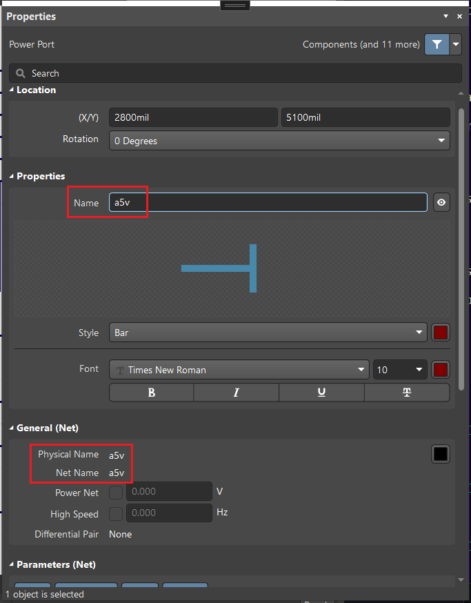
Altium Export Errata
- Any CustomLayer geometry will not be exported by the current Altium exporter.
Altium Roundtrip Errata
These design features are not preserved in JITX.
- In the Altium project generated by JITx, microVias are not distinguished from regular vias.
There are several parameters of an Altium project, which are not preserved in the Altium project generated by JITx.
- The View options for View Configuration of PcbDoc are not preserved, such as transparency level (default to 0) and the layout mode (default to "Altium Standard 2D").
Kicad Importer Errata
There are several known limitations/issues of Kicad importer.
-
A through-hole pad uses all copper layers. The other connection options are not supported.
-
Power Symbols:
- A Power Symbol, represented with the "#PWR" prefix in the Reference property, is attached to the net, specified in the Value property, on any sheet.
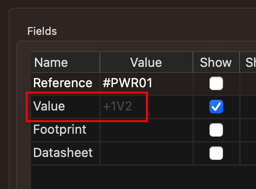
- A Power Flag Symbol or an Annotation Symbol, represented with the "#FLG" prefix or the "#SYM" in the Reference property respectively, are ignored.
- A Power Symbol, represented with the "#PWR" prefix in the Reference property, is attached to the net, specified in the Value property, on any sheet.
Tutorials
Tutorials are small, rewarding projects that will help you build confidence and start developing a mental model for how JITX works. These are intended to be self-contained, introductory projects for learning.
JITX Workflow
The following is the end-to-end workflow of going from an idea to a design using JITX.
- Define requirements (Conventional EE process).
- System level design / block diagram (Conventional EE process).
- Create a new JITX project.
- Pull in major components to your JITX project.
- Import your components from an existing design or component file (KiCad or Altium).
- Search OCDB to see if the part exists.
- Connectivity + Passives
- use
netstatements to connect your components together - use
res-strap,cap-strap, etc. to create passives, pullups, etc.
- use
- Checks
- write checks for your components and design, then run them to verify validity of your design
- Export to CAD (Altium or KiCad)
- Layout, Order Board (Conventional EE process)

Learning JITX - What To Do When You're Stuck
Here are some tips to follow when you're stuck/don't know how to do something in JITX.
Quickstarts (Start Here)
These are fast-paced tutorials that will bring you from 0 knowledge of JITX to designing full electrical design in code.
Quickstart 1: Your First JITX Design
NOTE: Before starting this tutorial, you should have installed and set up JITX.
Introduction
Welcome to JITX! This Quickstart tutorial is your gateway to faster hardware and PCB design.
In this tutorial, we will guide you to create your very first "smart" power regulator circuit to meet your design requirements automatically. This is a critical time saver for our JITX hardware engineers.
Using the code-based approach, we will:
- generate circuits that can adapt to changes in your requirements
- create schematics and PCB designs that are correct (due to intelligent code).
- update circuit components using a single line of code.
- accelerate your PCB design and layout speed by over 70%.
You typically can't find this kind of power embedded in any other ECAD tool!
So let's get started!
What is JITX?
JITX is a groundbreaking electronic computer aided design (ECAD) software that empowers electrical engineers to design electronics hardware and printed circuit boards (PCBs) faster using code.
This code-based approach to electronics and PCB design takes a lot of manual work out of schematic and PCB design, hence why JITX ends up giving a way faster workflow than normal for industry.
Before We Begin
First you need to install JITX. If you haven't done this yet, please refer to our JITX installation guide on the JITX website. Once JITX is up and running on your computer, you're ready to roll!
Overview
In this Quickstart Tutorial 1, we cover a lot of ground. You will
- Geting to Know JITX - Become familiar with the JITX workspace
- Create a simple design we will just call Design 1
- Learn the complete flow to design a printed circuit board (PCB)
- Generate a second design we just call Design 2 (our adaptive power regulator)
As we go through the tutorial, not only do you get a refresher on the PCB design process, but you see exactly how JITX introduces faster ways to do ECAD for printed circuit board design. Also, you will be given a number of exercises you can do to get you familiar with JITX and VS Code.
1. Getting to Know JITX
Navigation
In this section you will learn where to find your project files, which windows are important in JITX and which mouse and button commands you need to work a design.
TIP: The Terminal window. In VS Code, there is a terminal that lets you execute commands - similar to Windows PowerShell or Mac OS Terminal. The terminal is useful not only for executing commands in JITX software, but for debugging your own design code.
To get comfortable with the terminal, let us do our first exercise.
Exercise 1
Your first exercise is to open the terminal window in VS Code.
To open the terminal, in VS Code, select the menu item View - Terminal (or type Ctrl + ` on your keyboard).
Once done, a terminal window should appear at the bottom of VS Code as seen below.

Then the text in the terminal will tell you which user is logged into the machine and who is executing the commands.
Type the following command, such as dir if you are in Windows or pwd if you are on Mac OS or Linux.
Depending on your operating system, you will see the name of your current directory.
Mine shows:
kirschmackey@Kirschs-MacBook-Air ~ % pwd
/Users/kirschmackey
Once your terminal shows the directory you are working in and prints it to the terminal, you have successfully executed the command.
Close the terminal window by clicking on the 'X' icon at the upper right corner of the terminal window shown below.

The Terminal disappears.
Exercise 1 - Done
Points Acquired = 2 points
Exercise 1 Takeaway
In JITX we are working with code now. In some cases, you will need to debug design behavior and compilation errors using the VS Code terminal window.
In upcoming tutorials when we say to 'run a command', we are referring to the VS Code terminal.
Next let's look at the different views of your design.
Window Views of Your Design
As you build your design, you have to look at the schematic, board layout, and files within your design to know if what you wrote in code is correct. To do this, click the JITX logo on your VS Code window (ours is on the far left).
That will make the JITX menu options and the Views section visible (see below).
![]()
View Icons in jitX
These icons are important for verifying your design schematic and PCB layout at any time. We are ready for another exercise.
Exercise 2 - Design Views
In this next exercise, you will see which windows appear upon clicking the icons.
Step 1
First, click the Schematic icon. You should get an error message at the lower right of VS Code saying there is no schematic to show and to run a design containing view-schematic(). Later in our example design you will see the code that generates a schematic.
Step 2
Next click the Board icon. You will get an error message saying there is no board to show and to run a design containing view-board(). Later in our example design, you will see that there is a line of code that creates a board view.
Step 3
Still in the Views section from the previous photo, click the Checks icon. In this case, a window appears at the bottom, and multiple Panel tabs are open (see below).

The highlighted panel is the 'JITX CHECK REPORT: CHECK REPORT' panel. Notice there are other panels as well, such as 'TERMINAL' (we were just in there in Exercise 1), 'PORTS', and so on. Click on each of those panels and observe what happens.
Step 4
Finally, click the Explorer button under our Views section.
You will see the 'JITX COMPONENTS' Panel appear at the bottom of the VS Code screen. This is our Open Components Database (OCDB) - a searchable, real-time components database that you can pull components from and use in your own designs.
Exercise 2 - Done
Exercise Points Acquired = 4 points
Exercise 2 Takeaway
Knowing how to navigate your design tool is critical for getting your designs finished faster.
Now that you have been introduced to the the JITX user interface, you are ready to create our first design.
2. Design 1 - Intro to JITX By Example
Let's get started with your first design.
Creating a New JITX Project (Example)
We are going to create a PCB design from scratch.
In the JITX VS Code panel, let's kick things off:
-
Click the JITX app icon (if you already see Design Tools in the image below then no need, else it will close JITX. If you clicked anyway when it was open, just click the app icon again to make the Design Tools section in the picture below visible again)

-
Create a new 'parent folder' to hold your designs in by going to menu File - Open (if you already created a folder) or File - New if you need to make a new folder.
-
You can name the parent folder something like Quickstart1, similar to mine below:

-
Once your new parent folder has been created or selected, click the Select Parent Folder button.
-
This will populate the Parent Folder with the directory of the folder you just created.
-
Create a new project by clicking under the Design Tools section and choosing New Project You will see a dropdown appear

-
In the Project Name field, give your project a descriptive name, such as "regulator-tutorial."
-
Then hit the Submit button.
JITX will open a new window in VS Code that points to a new folder created, named after whatever project name you chose. In this example, it created a folder named "Regulator-Tutorial".
New Files Created
Not only does a new VS Code window open to your new project folder, notice that new files were created.

Let's get familiar with these files by doing some exercises.
Understanding What main.stanza Does
Each file in your design folder has important functions. We will explain each one briefly so that you are comfortable when modifying the main project file later on. Let's look at the most important file - the main project file, main.stanza
Main.Stanza
main.stanza is the main program file from which you run your entire design. The .stanza file is also where you define your electrical circuits and PCB. It even pulls functions from other coding files, like helpers.stanza.
We will break down main.stanza quickly so that you immediately understand what it is doing, then can make some modifications based on that knowledge. Here is an initial breakdown in the image below:

Main.Stanza - Functional Breakdown JITX made this example project and it is broken down into these sections:
-
Import major libraries, functions and commands (just like introducing header files in c programming)

-
Board dimensions and definition (shape, size, etc.)

-
Declaring the functional block diagrams (groups of circuits to execute those functions) - these are similar to declaring functions you want inside a main coding file.

- Adding components (electrical and/or mechanical) for those circuit groups (uses the JITX components database)


- Set PCB Fabricator and Board shape

- Set the schematic sheet parameters

- Set the main top level module for the design

- Finally view the schematic and PC board for layout

Now that we have a breakdown of the main.stanza file, we can move on to the next section. To solidify these concepts, you can perform the following exercises.
Exercise 3 - Creating Your Own main stanza file
Even though it may seem trivial, copying and pasting the code into a new file immediately after having the code structure explained will help you retain and understand the main.stanza details more effectively.
So in these exercise, we will make a clone of the main.stanza file by copying and pasting the example code into the new file and repeating the purpose of each code section.
-
Step 1 - create a new file in VS Code by click the menu File - New File
-
Then notice a top bar appear in VS Code awaiting the file name.
-
Name your file
main-exercise3.stanzaand you will get a new window below
-
Click Create File in the Finder window
Our new mock main project file has been created, it is visible in the VS Code interface and it is completely blank.

Let's build it together:
- Import major libraries and commands. Don't worry about where those come from yet as that is an advanced topic. To do this:
- Copy the code below:
defpackage main :
import jitx
import core
import jitx/commands
import ocdb/utils/generic-components
import helpers
import ocdb/modules/passive-circuits
- Paste it into your
main-exercise3.stanzafile. You have now imported high level functions and imported the open components database, plus access to some helper functions we will use later.
Let's repeat this process with the following code snippets.
- Declare the board dimensions. Copy the code below and paste it into your own
main-exercise3.stanzafile.
; Define the shape/size of the board
val board-shape = RoundedRectangle(30.0, 18.5, 0.25)
- Declare your functional block diagrams (which will eventually become circuit groups consisting of components, wired connections, etc.) - these are known as 'modules' in JITX.
pcb-module lm317a-regulator (output-voltage:Toleranced) :
pin vin
pin vout
pin gnd
pin adj
- Add/create components (whether in modules or not)
- 10 kΩ resistor
; Create a 10k resistor component
res-strap(power-5v, signal, 10.0e3)
- Mechanical component - label
; Write the board version on silkscreen
inst version-label : ocdb/artwork/board-text/version-silkscreen("Version 0.0")
place(version-label) at loc(0.0, height(board-shape) / 2.0 - 1.0) on Bottom
- Set the high-level design name
; Set the design name - a directory with this name will be generated under the "designs" directory
; the board - a Board object
; [optional] rules - the PCB design rules (if not givn default rules will be used)
; [optional] vendors - Strings or AuthorizedVendors (if not give default vendors will be used)
; [optional] quantity - Minimum stock quantity the vendor should carry (if not give default quantity will be used)
setup-design(
"jitx-design",
ocdb/utils/defaults/default-board(ocdb/manufacturers/stackups/jlcpcb-jlc2313, board-shape)
)
- Set the schematic sheet size
; Set the schematic sheet size
set-paper(ANSI-A)
- Package everything into a complete design and set that as the highest level module
; Set the top level module (the module to be compile into a schematic and PCB)
set-main-module(my-design)
- Publish/view the finished schematic, and the PCB layout generated from code
; View the results
view-board()
view-schematic()
view-design-explorer()
Once you have copied and pasted those lines of code into your own main-exercise3.stanza file, you should end up with ~46 lines of code, because it will be missing the code to do design checks (shown below):
; Use any helper function from helpers.stanza here
; run-check-on-design(my-design)
Why did we skip this snippet of code? Because we will not be executing Checks on the designs in this guide.
Also notice that this code snippet was commented out (in JITX, code is commented out using the semicolon character at the beginning of the line).
Deleting a File
In VS Code, Right click your main-exercise3.stanza file, then choose Delete from the drop down menu. Your file you just made will be deleted. We no longer need it for this Guide.
Exercise 3 - Done
Points Acquired - 18 pts (2 pts per copied and pasted code)
What You Learned
JITX establishes its designs using code.
- You understand the structure of a typical example code-defined schematic + PCB layout project in JITX
- you can import functions
- call components from a database of existing JITX components that we open to the community.
- JITX turns all designs into modules that can be used later
- you can declare the board size and the schematic sheet size
- You know how to create files using the VS code interface directly
- You know where to find your design files in VS Code
As an optional exercise, you are encouraged to click the other files in your folder, such as helpers.stanza, and stanza.proj and guess what they help your design to do.

You can also click one of the files, and choose to Reveal in Finder (Mac OS) or Explorer (Windows OS). That will open the folder and show that new folders were created in your project folder as well, containing many .stanza files, components, folders for 3D models, etc.
Now that you know there is a lot more than meets the eye with simple project creation (multiple folders and files are generated to make a project), the next step is to generate the schematic and PCB layout views from the Design 1 code.
Design 1 - Generating the Schematic and PCB
With your code in place, it is time to bring your design to life.
In the previous exercise, by making a new project, you you created simple PCB code that contained a resistor and a label.
Now it’s the moment of truth - we will generate the schematic and PCB layout view for design 1!
With the main.stanza file active in VS Code, click anywhere inside the code, then press Ctrl + Enter to run the program (use the left keyboard Ctrl key instead of the right Ctrl key).
JITX compiles your design and generates a schematic and board in the PCB layout panel below.

Note that just like above, you may see a blank design in the "JITX VISUALIZERS: BOARD". To correct this, click the ![]() icon show in the image below (upper left side of VS Code terminal Panel amongst other icons).
icon show in the image below (upper left side of VS Code terminal Panel amongst other icons).

Once the icon is clicked, your PCB view will zoom in like below:

You generated a schematic and a printed circuit board using a frew lines of code instead of using manual graphically drawn methods (typical EDA flow).
Key Takeaway
Using code to generate a physical design and schematic is a game-changer. It's faster and more efficient than manually moving components around. Your time is precious, and JITX ensures you make the most of it.
About the Schematic - The schematic, is the upper left view in the image above. Once generated, the schematic cannot have its connections edited graphically. You can click in the schematic window, drag components around withe left mouse button, pan using the right mouse button, and zoom using the scroll wheel. However, it is impossible to modify the connections from the schematic view. In JITX, we prevent net adjustments via schematic view to prevent design mistakes and to maintain the correctness of the original design (which is defined using the code instead).
Tip: Initial Schematic View - Your schematic and PCB views may not show the components up close, so you may need to zoom in (Scroll Up while in the window) and pan (Hold and drag the canvas with the right mouse button) to see the part(s) more clearly.
About the PCB - You can also click around, zoom and pan in the PCB view. When you select the resistor 'R1' in the layout, it gets highlighted in the schematic view as well. This behavior is commonly known as 'cross-probing' in ECAD tools.
Alright, so congratulations on generating your first schematic and PCB layout using code!
In the next section we will show you how to make changes to your schematic and board (an Engineering Change Order) using code. Then that will complete Design 1 in this guide.
Engineering Change Order (ECO)
In practice, hardware designs often require changes or updates after the PCB has been created, even after PCB routing has started. This kind of change is called an Engineering Change Order (ECO) and while it may happen at any phase of the PCB design process, it is progressively more expensive to implement during later stages of the design.
Exercise 4 - Engineering Changes and Updating Code
In any case, let us say our design needs a couple tweaks based on customer feedback. That means we need to perform an ECO.
Removing Components via Comments
First let us remove components. To remove a part/component from a design, simply delete (or comment out) the code.
For instance comment out the res-strap(power-5v, signal, 10.0e3) line by placing a semicolon (;) at the start of the line.
Then while still in the code, hit Ctrl+Enter (and give JITX time to refresh), your resistor disappears from the schematic and the PCB.

Changing a Component Value
Then let’s say we need to update the version of the design that has no resistor. We should change the label from 0.0 to 0.1. To do that, change the Version 0.0 text to Version 0.1 in the code below.
; Write the board version on silkscreen
inst version-label : ocdb/artwork/board-text/version-silkscreen("Version 0.0")
place(version-label) at loc(0.0, height(board-shape) / 2.0 - 1.0) on Bottom
You should end up with this code:
; Write the board version on silkscreen
inst version-label : ocdb/artwork/board-text/version-silkscreen("Version 0.1")
place(version-label) at loc(0.0, height(board-shape) / 2.0 - 1.0) on Bottom
After the change, perform that ECO again by making sure your cursor is anywhere inside the code window, and regenerating with Ctrl+Enter.
Then voila! Your design label has been updated in the schematic and the PCB layout!

Excellent. You completed exercie 4!
Exercise 4 - Skills Attained
In this exercise you learned how to make changes to your code and regenerate your schematic and PCB design. Some things to rememeber are:
- you can comment code using semicolons
; - you can also delete the code
- to commit changes to your design graphically, type
Ctrl+Enter(using the left Ctrl key)
Exercise 4 Points Acquired = 3
Exercise 4 - Done
Design 1 Finished
Now that you have finished your first design and gotten familiar with JITX, let's jump into the second design in this guide.
Part 2 - The PCB Design Process and Your Second Design
In the previous part of this guide, you became familiar with JITX, how to navigate the tool and how to generate and update a design.
In this Part 2, you will learn a lot more about the practical applications of using JITX for PCB design. We will cover:
- The standard hardware design process
- How to use JITX to implement a simple design
3. The Standard Hardware Design Workflow - Idea to Manufacturing
The following is the end-to-end workflow of going from a product idea to a PCB design. Then in the design 2 example, we show you how to implement this using JITX more quickly than it would take if done graphically like one would if using existing ECAD software.
Hardware Design Process + Powered by JITX
- Define requirements
- System level design, then a block diagram
- Create a new JITX project (in JITX, the project files are all modifiable code)
- Pull in major components to your JITX project (JITX components are taken from a live database so you don't have to spend as much time searching for the right solution).
- Import your components from an existing design or component file (KiCad or Altium).
- Search our online database to see if the part exists.
- Create the component if it does not exist. (Using JITX component development, even the parts and their pins have intelligent data to inform your design and schematic to correctness.)
- Connectivity + Passive Components
- Note your nets,
- Wiring - Connect your component pins and nets together
- Perform PCB layout creation
- Modify and update the PCB graphically and programmatically (make quick work of tedious tasks that normally take forever using traditional methods, like routing DDR)
- Perofrm robust design checks
- write custom electrical checks for your components and design
- run them to verify the validity of your design from JITX's deep understanding of your circuit and component behavior - not just general electrical checks in a typical ECAD flow.
- Perform final touch-ups in other ECAD tools
- Export your PCB design to another software
- do final touch-ups after doing the bulk of the work quickly in JITX (you can export to Altium or KiCad)
- Manufacture the PCB
- Generate manufacturing files (Gerber, ODB++, IPC-2581, etc.)
- Order the Board from your favorite manufactuer
That is the general flow, but when it comes to JITX, steps 3 through 7 are defined using code and certain tasks are automated. This code-based automation and optimization leads to more robust checks that don't rely on human review, reducing the likeihood of human error in a design.
The following section of this guide will be your soft introduction to the JITX workflow to design PCBs, so that you become even more familiar with the new environment. Future tutorials will focus on more advanced tasks.
It is highly recommended that you complete the previous design first and do not skip ahead, because we build on the knowledge from previous exercises. So if you skip ahead you will have to backtrack to these steps anyway.
Okay with that out the way, let's start the EE process for PCB design using JITX!
4. Design #2 - PCB Design Process using JITX
As mentioned in section 3, we will use JITX follow the 9-phase process that one typically follows to design PCBs from scratch.
Phase 1: Define Requirements
This is just like any hardware design flow. We work with new design requirements, like power consumption, voltage output, current consumption and so on. To keep things simple, we want the following:
- a voltage regulator that generates an output voltage of 3.3 V at ±15%
- a voltage divider on the output pin that can sink a maximum current of 1.6 A.
More precisely, we want a design like the LM317A power regulator shown below.

Phase 2: System Level Design (Block Diagram)
The first step to any hardware/PCB design is to draw a system block diagram. The benefit of doing this is to ensure we include all 'functions' within the product so that our reaquirements are met.
The electronics or electrical design engineer would fill in those details eventually.
For example, the voltage divider and its optimal resistors would be calculated manually or using some tools outside the schematic capture environment.
What is a 'Module' in JITX?
Still on the functions aspect, those can be drawn as block diagrams and can then be considered 'modules' that can be used specific to this design, or that can be reused in other designs.
Understanding Modules Better
Therefore, a 'module' in JITX refers to a functional block that consists of components that are connected to each other. You can have, say, the power regulator, some resistors and capacitors all in a single power module (or function block), because they connect together to perform a certain circuit design. The benefit of this approach is to have a library of these best known circuits for various applications, so engineers don't have to redesign them every time they want, say, a power regulator circuit for 3.3V output.
Design reuse is not a new concept, as other ECAD tools also have ways to reuse circuit designs. However, JITX's library of adaptable circuit modules really takes reuse to the next level, because our circuits are universal and adapt to the design at the time of use.
That means you are no longer locked into reusing circuits for a single ECAD tool, but can use the same circuit in many.
That also means, that with our circuit generators, you do far fewer design calculations to get, say, the right set of resistors for a simple voltage divider. What's even better is that the larger our circuit library becomes, the more engineering hours we will save engineers worldwide.
In fact, this is one of the our missions - to make life easier for hardware designers everywhere. We also have a community dedicated to this dream for all EEs and PCB designers. If you would like to support the mission and create Circuit Generators and modules that anyone can use, ask to join our community and we will show you how to get started.
On that note, let's start adding some modules to our design.
Phase 3: Creating a Design/JITX Project
Exercise 5 - Adding A Module
First we want to add a module to the design. Which is executed by the code:
pcb-module lm317a-regulator (output-voltage:Toleranced) :
pin vin
pin vout
pin gnd
pin adj
And generates the overall design, but without the ports/pins ‘vin’, ‘vout’, ‘gnd’ or ‘adj’ being visible, as seen below.

Exercise 5 - Done
Exercise 5 Points Acquired = 2 points
You just added your first module!
Exercise 5 - Skill Acquired
Now that you know how to create modules, you will make additional modules (which would contain circuits) as you add components and flesh out the rest of each module in this design.
Phase 4: Components
Now we are in the Components design phase, where we start adding parts to our module(s).
Let’s say your engineering manager wants to add a power regulator, capacitors and a couple resistors to the board based on the LM317A, like the one below.

Typically this requires hand calculations for say, the voltage divider circuit, parametric searches online for the perfect component that meets our requirements and is at a reasonable price.
That process can take a solid one to two hours. That would involve making an Excel spreadsheet comparing all the different viable options, not to mention compliance to safety or perofrmance standards.
It is all too common for engineers to have to work with multiple environments, tools, websites and various files just to bring their design data together all at once.
Add in looking through each datasheet for the components being analyzed, this expedition could easily become an afternoon's worth of work.
Fortunately with JITX, you will not have to do as much heavy lifting, because JITX and the code environment will pull the proper component(s) for your application based on intelligent design requirements. This adaptability saves you the hassle of doing all that parametric analysis manually.
To understand this concept, let us do an exercise.
Exercise 6: Instantiating Smart Parts from JITX Component Database (OCDB)
Instantiating a Part
The second step is to instantiate a part (the LM317A) from our existing database and put it into the module we created earlier for the LM317 circuit. So to get this device:

We use the code below:

Here’s the code snippet for you to copy:
inst lm317a : ocdb/components/unisonic/LM317A/component
net (vin lm317a.input)
net (vout lm317a.output)
TIP: Be sure to indent this code at the same level as the
pinstatements above it. These components, pins and nets are all supposed to be within thepcb-modulefunction.
The LM317A gets instantiated. Next we need to wire this component back to the main design ports.
End of Exercise 6
Exercise Points Acquired = 3 points
Skills Acquired
In this exxericse you learned how to:
- Add a component to your design and
- Connect the pins of the component to other nodes
Exercise 7 - Adding Components. Capacitors
To add capacitors to your regulator or any device, we just need two lines of code. Then JITX will choose our capacitors for us based on the values given to it and with awareness of the LM317A recommendations as well.
Here’s the code to copy if you want to try it:
cap-strap(lm317a.input, gnd, 0.1e-6)
cap-strap(lm317a.output, gnd, 1.0e-6)
Be sure to indent these lines of code so they are one level more indented than the pcb-module command (or on the same level as the net commands just before this section). As a guide of the complete module code, you can use this below:
pcb-module lm317a-regulator (output-voltage:Toleranced) :
pin vin
pin vout
pin gnd
pin adj
inst lm317a : ocdb/components/unisonic/LM317A/component
net (vin lm317a.input)
net (vout lm317a.output)
cap-strap(lm317a.input, gnd, 0.1e-6)
cap-strap(lm317a.output, gnd, 1.0e-6)
JITX is awesome because you don't have to do so much parametric searching for components, especially for things like passive devices (resistors, capacitors, etc.). The library does that for you. Just define the parameters and it will find what you need!
End of Exercise 7
Exercise 7 Points Acquired = 2
Even if component selection is taken care of by JITX, multi-component circuits that make a certain topology requires a special kind of code.
Next we will select a voltage divider and have JITX calculate our resistor values for us (based on components available in the Open Components Database (OCDB). We also discuss the typical approach to hardware design and why the new approach saves a lot of time.
Typical Approach to Circuit Design...
Normally, you would have your requirements defined, for your voltage divider, for example. To do this you would:
- have to do component research,
- pull up a spreadsheet,
- do some analysis on the proper resistor value selection based on hand calculations for the ideal feedback voltage,
- then select parts based on what’s available in component databases.
- then back-calculate new values based on what resistors you could find on the market
All of this work is to find a few capacitors.
Luckily JITX has a solution for this, which we call Circuit Generators.
Modern Approach - Lessen Your Design Work by Using JITX Circuit Generators
You have encountered the next cool thing about JITX for automation in hardware design - Circuit Generators. Occasionally, we might refer to these generators as solvers for short.
Circuit generators are snippets of code that automatically select comopnents to meet your design requirements (e.g. a voltage divider) in terms of voltage, current and power consumption.
Circuit Generators are part of a special library of code (shown in next example). They reduce tedious tasks mentioned in the previous sedction and only require a couple lines of code. Circuit generators can turn what would take a couple hours of manual work into seconds.
To see this in action, let us select a generator and run it.
Exercise 8 - Use a Circuit Generator
First we want to implement the the kind of circuit seen below.

To do this, copy and paste the following code into the design.
Voltage divider Circuit
inst output-voltage-divider : voltage-divider(source-voltage = output-voltage,
divider-output = 1.25 +/- (15 %)
current = 5.0e-3 )
Quick explainer of the code:
voltage-divider(source-voltage = output-voltage- this means we want the source of the voltage divider (going into the top resistor pin) is connected to theoutput-voltagecoming from the LM317A device we instantiated earlier.- for more information on how this works, consult this guide
divider-output = 1.25 +/- (15 %)- this means we want the node connecting the two resistors to each other to have 1.25 ± 15% V (minimum of 1.0625 V, maximum of 1.4375 V) coming out of it.current = 5.0e-3 )- this is the maximum current (5 mA) we allow through the two resistors.
Eventually when we generate Ctrl+Enter the new design, the solver will do its thing and pick the resistor network (best resistors for the job within a certain tolerance of the desired output voltage) for us. It can do this, because it has enough information, like the output voltage coming from the LM317A's output pin, and our desired output from the divider.
We have our components, so now let us connect them.
Exercise 8 - Done
Exercise 8 Points Acquired = 2
Exercise 8 Skills Acquired
You learned how to instantiate (use) a circuit generator in a design. There are multiple kinds of circuit generators (or 'solvers') that help automate your design flow and will only grow as time progresses and engineers add more to our libraries.
The next step is to connect our circuits.
Phase 5: Connectivity
Remember that code at the top of the project that made a PCB module with the pins ‘vin’, ‘vout’, ‘gnd’ and ‘adj’ that we couldn’t see?
In this step, we’re using the net command to connect those unseen pins/ports to the input and output pins of the LM317A. The end result will have no visual change to the design.
In the next exercise, we will connect the voltage divider to the pins of the LM317 regulator.
Exercise 9 - Connecting nets
To connect component pins or nets, follow along by copying the code below:
net (output-voltage-divider.in lm317a.output)
net (output-voltage-divider.out lm317a.adj adj)
net (output-voltage-divider.lo gnd)
and pasting it into the design window in VS Code underneath this code:
inst output-voltage-divider : voltage-divider(source-voltage = output-voltage,
divider-output = 1.25 +/- (15 %)
current = 5.0e-3 )
Making sure that the net commands are in line with the inst command. That means your code so far for the entire design from the top would look like this:
#use-added-syntax(jitx)
defpackage main :
import jitx
import core
import jitx/commands
import ocdb/utils/generic-components
import helpers
import ocdb/modules/passive-circuits
; Define the shape/size of the board
val board-shape = RoundedRectangle(30.0, 18.5, 0.25)
pcb-module lm317a-regulator (output-voltage:Toleranced) :
pin vin
pin vout
pin gnd
pin adj
inst lm317a : ocdb/components/unisonic/LM317A/component
net (vin lm317a.input)
net (vout lm317a.output)
cap-strap(lm317a.input, gnd, 0.1e-6)
cap-strap(lm317a.output, gnd, 1.0e-6)
inst output-voltage-divider : voltage-divider(source-voltage = output-voltage,
divider-output = 1.25 +/- (15 %)
current = 5.0e-3 )
net (output-voltage-divider.in lm317a.output)
net (output-voltage-divider.out lm317a.adj adj)
net (output-voltage-divider.lo gnd)
Now let's explain what we just added:
Explanation of Net Command
The first net command says to connect some nets (or pins of components) together. The nets/pins in this case are:
- the source/input of the voltage divider to the output pin of the LM317A
- the output of the voltage divider to the adjustment feedback pin of the LM317A
- the bottom pin of the voltage divider to the ground net
So instead of drawing wires like in a regular ECAD tool, we can explicitly state which nets, pins and nodes we want connected to each other, without room for graphical error.
Now that the voltage divider has been connected to the LM317 regulator, we have come to learn from the datasheet that this LM317A device needs capacitors on the input and output pins.
Alright, the voltage divider circuit is connected. Next step is setting our main design output voltage.
Exercise 9 - Done
Exercise 9 Points Acquired = 4 points
You now know how to connect nets and pins of circuit elements to each other.
(Optional) Updating the Board Version
To update your board version, give it any number you want. Considering ours was a demo, we will just keep it at 0.0 for now.

Here is the code to make a label that has the version you want on it, and (just to be safe) a definition of our board design:
; Module to run as a design
public pcb-module my-design :
val target-voltage = 3.30 +/- (10 %)
inst reg : lm317a-regulator(target-voltage)
; Write the board version on silkscreen
inst version-label : ocdb/artwork/board-text/version-silkscreen("Version 0.0")
place(version-label) at loc(0.0, height(board-shape) / 2.0 - 1.0) on Bottom
Make sure that if you copy and paste this code, that the ; Module to run part is aligned with the pcb-module lm317a-regulator (output-voltage:Toleranced) :
code snippet this time. The reason being that our label, and other code being pasted is not part of the voltage regulator circuit module we made. The label and whatnot are part of the larger design that encloses everything.
To make sure we're on the same page, here is the code you should have so far:
#use-added-syntax(jitx)
defpackage main :
import jitx
import core
import jitx/commands
import ocdb/utils/generic-components
import helpers
import ocdb/modules/passive-circuits
; Define the shape/size of the board
val board-shape = RoundedRectangle(30.0, 18.5, 0.25)
pcb-module lm317a-regulator (output-voltage:Toleranced) :
pin vin
pin vout
pin gnd
pin adj
inst lm317a : ocdb/components/unisonic/LM317A/component
net (vin lm317a.input)
net (vout lm317a.output)
cap-strap(lm317a.input, gnd, 0.1e-6)
cap-strap(lm317a.output, gnd, 1.0e-6)
inst output-voltage-divider : voltage-divider(source-voltage = output-voltage,
divider-output = 1.25 +/- (15 %)
current = 5.0e-3 )
net (output-voltage-divider.in lm317a.output)
net (output-voltage-divider.out lm317a.adj adj)
net (output-voltage-divider.lo gnd)
; Module to run as a design
public pcb-module my-design :
val target-voltage = 3.30 +/- (10 %)
inst reg : lm317a-regulator(target-voltage)
; Write the board version on silkscreen
inst version-label : ocdb/artwork/board-text/version-silkscreen("Version 0.0")
place(version-label) at loc(0.0, height(board-shape) / 2.0 - 1.0) on Bottom
Okay, and when that's up to date, you should be clear to continue to the PCB layout phase.
Phase 6: PCB Layout
PCB Generation
The final step in the creation phase is to generate the design.
Exercise 10 - Generating an Intelligent PCB Design
To do that, make sure you have the final correct code (copy and paste the code below just to make sure).
Final Power Regulator code:
; Generated by JITX 2.25.0
#use-added-syntax(jitx)
defpackage main :
import jitx
import core
import jitx/commands
import ocdb/utils/generic-components
import helpers
import ocdb/modules/passive-circuits
; Define the shape/size of the board
val board-shape = RoundedRectangle(30.0, 18.5, 0.25)
pcb-module lm317a-regulator (output-voltage:Toleranced) :
pin vin
pin vout
pin gnd
pin adj
inst lm317a : ocdb/components/unisonic/LM317A/component
net (vin lm317a.input)
net (vout lm317a.output)
cap-strap(lm317a.input, gnd, 0.1e-6)
cap-strap(lm317a.output, gnd, 1.0e-6)
inst output-voltage-divider : voltage-divider(source-voltage = output-voltage,
divider-output = 1.25 +/- (15 %)
current = 5.0e-3 )
net (output-voltage-divider.in lm317a.output)
net (output-voltage-divider.out lm317a.adj adj)
net (output-voltage-divider.lo gnd)
; Module to run as a design
public pcb-module my-design :
val target-voltage = 3.30 +/- (10 %)
inst reg : lm317a-regulator(target-voltage)
; Write the board version on silkscreen
inst version-label : ocdb/artwork/board-text/version-silkscreen("Version 0.0")
place(version-label) at loc(0.0, height(board-shape) / 2.0 - 1.0) on Bottom
; Set the design name - a directory with this name will be generated under the "designs" directory
; the board - a Board object
; [optional] rules - the PCB design rules (if not givn default rules will be used)
; [optional] vendors - Strings or AuthorizedVendors (if not give default vendors will be used)
; [optional] quantity - Minimum stock quantity the vendor should carry (if not give default quantity will be used)
setup-design(
"jitx-design",
ocdb/utils/defaults/default-board(ocdb/manufacturers/stackups/jlcpcb-jlc2313, board-shape)
)
; Set the schematic sheet size
set-paper(ANSI-A)
; Set the top level module (the module to be compile into a schematic and PCB)
set-main-module(my-design)
; Use any helper function from helpers.stanza here
; run-check-on-design(my-design)
; View the results
view-board()
view-schematic()
view-design-explorer()
Then click anywhere inside the code in JITX, then hit Ctrl+Enter (generate) on your keyboard. Then voila, the design will take some time to load (even up to 30 seconds depending on how difficult it is for the Circuit Generating to find a solution for the voltage division circuit).
You will know you're on the right track if your output TERMINAL panel at the bottom of VS Code (you might have to click it) looks similar to below:
Current working directory: "/Users/kirschmackey/Documents/JITX/JITXProjects/Quickstart1/QS1_PowerRegDesign"
Loading JITX Shell...
-> Tolerance 2.0%
No solution.
-> Tolerance 1.0%
- Querying resistors for R1=442.0Ω R2=270.0Ω
Checking solution for existing components with: tol1=MinMaxRange(min=-0.01, max=0.01), tol2=MinMaxRange(min=-0.01, max=0.01)
Solved: mpn1=CRCW0402442RFKED, mpn2=RMCF0402FT270R, v-out=(min=1.0625V, nom=1.25V, max=1.4375V), current=0.00462962962962963A
Saving stable design and reference designator table
REPL environment is now inside package main.
Once finished, here are what the final schematic and PCB should look like:

Exercise 10 - Done
Exercise 10 Points Acquired = 2 points
Exercise 10 Skills Acquired and lessons learned
You have succesfully executed the creation of a design that has intelligence in it, due to the circuit generator solving and finding resistors for your design.
In the Routing and layout phase, we show another time-saving feature - autorouting!
Key Benefits in Design Phase and Modern JITX Approach:
- JITX has solvers that automatically select components for you for multiple applications
- What would normally take 30 minutes to complete now only takes JITX 5 seconds
- Design integrity is maintained by using a code-driven approach
- Design flaws are inherently reduced as circuits are based on solvable electrical calculation solutions and not based on graphics-only designs that could introduce unsolvable circuits
- Modular approach to the code libraries in JITX bodes well for design reuse and increasingly shorter design cycles (roughly 70% less time to manufacturing)
The next step is component placement.
Component Placement
Components have been placed onto the PCB and now it is time to connect them all using our router.
However, instead of manually routing traces by hand, we’ll use the routing tools inside JITX to do the routing for us.
Here is the unrouted board we generated:

Next I will manually rearrange the components by clicking and dragging them into new positions (hitting ‘R’ on my keyboard to rotate them while dragging them).
Tip: To properly select components on the PCB, hover your cursor over the land pattern so that a white box appears around that part. Then click (and hold if you wish) once you see the white box. That part will turn green to let you know it has been selected. If you clicked and released the mouse button, the part will still be green. To move the part, simply click hold and drag the mouse, and the part will attach to your cursor and move wherever you like. The important thing is that you do not need to click, release, then click-hold-drag. Simply click and hold (the green highlight will appear if you selected the part properly by seeing the white enclosing box on mouse hover first), then drag.

Excerise 11 - Component Placement
Rearrange the components in a way you would like them placed, taking note of the net names and rats nest lines (or 'airwires') that guide you on which pins should connect to which nets.
Exercise 11 - Done
Exercise 11 Points Acquired = 6 points
Exercise 11 Skills Acquired
In this exercise, you practiced moving components around on the PCB, so, component placement. Placement matters, so getting it right will make all the different in routing and the rest of layout.
Now that the components are positioned the way I want them to be, I can route them.
Note: JITX can auto place components as well, depending on your design preferences and goals, but we will save that cool feature for future guides.
Routing and Automation
Routing components on a PCB can be a daunting task, but not with JITX. Learn how to use JITX's routing tools to save time and create a professionally routed board without manual intervention.
Select any two or more pads at the same time (using Shift+Click) that you want to route.

Then click the "Autoroute" button in the upper right corner, (or press "q" on your keyboard).

The pads will be routed immediately. Here's what it looks like if you move a few components and autoroute a few of them.

In this case, even though our full design got routed almost instantly. An engineer who designs power PCBs might not be happy with the routing!
But we will skip routing improvements for now for the sake of the guide.
What’s also great is that you can hover over a net and it will show the net name at the bottom of the PCB layout window.
Okay that’s a quick way to get a board done. The next step is to check to see if this board passes certain rules and constraints, both in the schematic design and the PCB layout.
We call these Design Checks in JITX.
Phase 7: Design Checks
This design is relatively simple/straightforward so we will skip this step for this design and do Design Checks in more advanced training eventually.
Phase 8: Final Edits in Other ECAD Tools
Once your design is complete and has passed checks, it is time to generate manufacturing files for your PCB. JITX streamlines this process, ensuring your design is ready for production.
1. Export Design to CAD
You can export your design files to Altium and/or to KiCAD, allowing you to work more efficiently in JITX, but still collaborate with engineers who are not using JITX.
Exporting to Altium
To export your design to Altium, just have the JITX plugin installed in Altium Designer and then have an Altium project opened.
There is a helper file that pulls in functions for extra tasks that help with our board design ecosystem. By default, the file exports to Altium. But we want to export to KiCAD, so we need to change its code.
In the helpers.stanza file, find altium in the export destination section shown below:
; ====================
; Actual Export design
; ====================
public defn export-to-cad () :
set-paper(ANSI-A4)
set-export-backend(`altium) ; set the CAD software for export to be altium (also supported: `kicad)
export-cad()
Exercise 12 - Exporting CAD Files
Update the export destination to kicad if KiCAD is preferred, or keep it the same if using Altium. Now save that helpers.stanza file using Ctrl/Cmd+S or File - Save.
Click anywhere in the same file and use Crtl+Enter to export to KiCAD (Altium has to be open if you try to export to Altium, else you may get an error).
After all your changes are made, return to main.stanza and press Ctrl + Enter again.
Go into the file ‘helpers.stanza’, in your project folder and scroll down to the section of code that says:
Now, in the JITX Shell (This is the VS Code Terminal window), type export-design() and hit Enter to generate CAD files and our bill of materials.
You will then get an output similar to this one below in the VS Code Terminal:
stanza> reload
-> Tolerance 2.0%
No solution.
-> Tolerance 1.0%
- Querying resistors for R1=442.0Ω R2=270.0Ω
Checking solution for existing components with: tol1=MinMaxRange(min=-0.01, max=0.01), tol2=MinMaxRange(min=-0.01, max=0.01)
Solved: mpn1=CRCW0402442RFKED, mpn2=RMCF0402FT270R, v-out=(min=1.0625V, nom=1.25V, max=1.4375V), current=0.00462962962962963A
Saving stable design and reference designator table
stanza> export-design()
Export to CAD starts ...
Saving stable design and reference designator table
Unable to realize uninitialized layer 0
Unable to realize uninitialized layer 1
Unable to realize uninitialized layer 2
Unable to realize uninitialized layer 3
Changes detected:
- 3 groups added: reg.lm317a-regulator, reg.output-voltage-divider.voltage-divider, false
Schematic group tree:
false
├─ reg
│ ├─ reg.lm317a-regulator
│ └─ reg.output-voltage-divider.voltage-divider
└─ false
JITX: Packing schematic groups into sheets.
Export to CAD is done. The output is located at: designs/jitx-design/kicad
The files were generated in the following folder inside your project folder (only if you chose the kicad option): NameYouGaveYourProject/designs/jitx-design/kicad. If you want to get there quickly, you can right click on any of the design files (e.g. main.stanza`), then choose to show in Finder (Mac OS) or Explorer (Windows OS).
Exercise 12 - Done
Exercise 12 Points Acquired = 2 points
Exercise 12 Skills Acquired
You now know how to export KiCAD (or Altium) design files so that others (or yourself) can modify and clean up existing routes, schematics, and so on in your own ECAD software.
Phase 9: Manufacturing the PCB
At this point you have generated either an Alitum or KiCad project, depending on the setting you chose in the previous section. In our case, we used KiCAD since we are on a Mac and running KiCAD.
Ordering the board (PCB, PCBA, etc.)
This is the step where you order the board from your preferred manufacturer. You would need the following:
- Design files
- Bill of materials (BOM)
- PCB Fabrication files (PCB, ODB++, IPC-2581)
The design files you would have generated from the previous section, Generating CAD Files. The PCB Fabrication files would come from the other ECAD tool you exported to after engineering creates them. You can generate a bill of materials (BOM) using JITX directly.
To do that, go back to the VS Code terminal window and run export-bom().
You will get an output similar to below:
stanza> export-cad
[Fn object]
stanza> export-bom()
Writing BOM to "designs/jitx-design/bom/jitx-design.xlsx" in XLSX format...
Writing BOM to "designs/jitx-design/bom/jitx-design.tsv" in TSV format...
It generated a .xlsx Excel BOM spreasheet and a tab-separated file (TSV). Open and examine those files and you can modify them as needed.
That ends the PCB design process and the different ways JITX can be used to execute the workflow.
5. Conclusion
Congratulations! You have successfully designed your first hardware project using JITX.
You now know how to:
- create new projects
- establish circuits as modules for modular design
- add components from our open components database
- use circuit generators to make adaptable designs (so you don't have to do so many calculations)
- wire components in a schematic
- generate PCBs using code and JITX
- place components in the JITX PCB environment
- route components using the autoroute feature
- export designs in JITX to other software (Altium, KiCAD)
- Generate a bill of materials (BOM)
Excellent work!
If you have been doing the exercises in this tutorial, you would have earned some points.
- Exercise 1 - 2 pts
- Exercise 2 - 4 pts
- Exercise 3 - 18 pts
- Exercise 4 - 3 pts
- Exercise 5 - 2 pts
- Exericse 6 - 3 pts
- Exercise 7 - 2 pts
- Exercise 8 - 2 pts
- Exercise 9 - 4 pts
- Exercise 10 - 2 pts
- Exercise 11 - 6 pts
- Exercise 12 - 2 pts
- Total Points = 50 pts
You are well on your way becoming Activated as a JITX User.
Here is the breakdown of the levels you can attain if you do the exercises in the tutorials:
- Learner Level (0 to 70 points)
- Initiate (0-33 points)
- Novice (33-50 points)
- Apprentice (51-70 points)
- Journeyman (71-90 points)
- Advanced Level (91 to 150 points)
- Expert (91-110 points)
- Master (111-130 points)
- Guru (131-150 points)
- JITX Champion (151+ points)
- JITX Jedi (200+)
In later guides, we will learn more about JITX, like how to organize our schematic, how to auto-place components based on design requirements or cost, assisted routing, signal integrity, and even pin swapping. Welcome to JITX.
Completed code for the Quickstart - Part 1: Your First JITX Design Tutorial
Also the starting code for the Quickstart - Part 2: Organize a Design Tutorial
; Generated by JITX 2.25.0
#use-added-syntax(jitx)
defpackage main :
import jitx
import core
import jitx/commands
import ocdb/utils/generic-components
import helpers
import ocdb/modules/passive-circuits
; Define the shape/size of the board
val board-shape = RoundedRectangle(30.0, 18.5, 0.25)
pcb-module lm317a-regulator (output-voltage:Toleranced) :
pin vin
pin vout
pin gnd
pin adj
inst lm317a : ocdb/components/unisonic/LM317A/component
net (vin lm317a.input)
net (vout lm317a.output)
cap-strap(lm317a.input, gnd, 0.1e-6)
cap-strap(lm317a.output, gnd, 1.0e-6)
inst output-voltage-divider : voltage-divider(source-voltage = output-voltage,
divider-output = 1.25 +/- (15 %)
current = 5.0e-3 )
net (output-voltage-divider.in lm317a.output)
net (output-voltage-divider.out lm317a.adj adj)
net (output-voltage-divider.lo gnd)
; Module to run as a design
public pcb-module my-design :
val target-voltage = 3.30 +/- (10 %)
inst reg : lm317a-regulator(target-voltage)
; Write the board version on silkscreen
inst version-label : ocdb/artwork/board-text/version-silkscreen("Version 0.0")
place(version-label) at loc(0.0, height(board-shape) / 2.0 - 1.0) on Bottom
; Set the design name - a directory with this name will be generated under the "designs" directory
; the board - a Board object
; [optional] rules - the PCB design rules (if not givn default rules will be used)
; [optional] vendors - Strings or AuthorizedVendors (if not give default vendors will be used)
; [optional] quantity - Minimum stock quantity the vendor should carry (if not give default quantity will be used)
setup-design(
"jitx-design",
ocdb/utils/defaults/default-board(ocdb/manufacturers/stackups/jlcpcb-jlc2313, board-shape)
)
; Set the schematic sheet size
set-paper(ANSI-A)
; Set the top level module (the module to be compile into a schematic and PCB)
set-main-module(my-design)
; Use any helper function from helpers.stanza here
; run-check-on-design(my-design)
; View the results
view-board()
view-schematic()
view-design-explorer()
Quickstart: Organize a Design
In this tutorial, we'll take the regulator design from Quickstart - Your First JITX Design and create a characterization fixture around it. We'll then add power and ground symbols and group together sections of the schematic using schematic-group. We'll also use layout-group so these same groupings happen in our layout.
NOTE: This Quickstart begins where the Quickstart - Your First JITX Design finishes. For your reference, the starting code for the file
main.stanzaand the finished code for this Quickstart tutorial are available.
Tutorial - Adding a Fixture and Organizing the Design
1. Building the Fixture
Let's add a pair of banana jacks to provide DC power. There is already a banana-plug-module() defined in ocdb/utils/generic-components (Ctrl+Click on the name in VS Code to go to its definition). This module places a red and black banana jack at a standard connector pitch, labels each, and then provides a power port as an electrical interface. The power port is a JITX bundle, which contains pins gnd and vdd.
We'll then connect the power pins or the banana jack to the regulator circuit via the net command, also naming the nets to be gnd and vin. You can only connect to ports of an instance like source after you instantiate it with an inst statement.
Add the following code inside the my-design module, after the instantiation of the lm317a-regulator (note the indentation):
inst source : banana-plug-module() ; shortcut to instantiate and place two `banana-plug`s plus the electrical support
net gnd (reg.gnd, source.power.gnd)
net vin (reg.vin, source.power.vdd)
Similarly, let's add an BNC connector to the regulator output after the code added from above.
inst measure : bnc-connector()
net vout (reg.vout, measure.sig)
net (gnd, measure.gnd)
We can then add test points to the adj pin, and gnd so we can inject some noise to this device and measure the change of the output. The function add-testpoint() modifies the calling module to add a ocdb/components/keystone/500xx component. Add the following code after the code added from above.
val test-points = add-testpoint([reg.adj, gnd])
Finally, we do some calculations to find a load resistor, and then pass the parameters to chip-resistor to select a part from the database (add the following code after the val test-points = ... ).
val target-current = 450.0e-3
val target-load = closest-std-val(typ-value(target-voltage) / target-current, 5.0)
inst load : chip-resistor(["resistance" => target-load, "min-rated-power" => typ-value(target-voltage) * target-current * 2.0 ])
net (load.p[1], reg.vout)
net (load.p[2], gnd)
Adding all that in and running the design (with Ctrl + Enter), we get this new schematic:
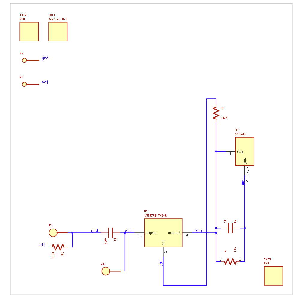
This schematic is technically correct, but not very legible. Let's add a couple lines of code to clean it up.
2. Handle Power Planes and Nets
We can add a ground plane to our design by adding this code to our main design:
; add a ground plane
geom(gnd) :
copper-pour(LayerIndex(1), isolate = 0.1, rank = 1, orphans = true) = Rectangle(width(board-shape) - 1.0, height(board-shape) - 1.0)
We can also specify trace width for various net classes. Let's do that for the power nets:
; add a net class for power nets
val power-net-class = NetClass(`Power, [`min-trace => 0.381])
property(gnd.net-class) = power-net-class
property(vout.net-class) = power-net-class
property(vin.net-class) = power-net-class
3. Net symbols
We can assign symbols to any net that we have named. Add symbols to the ground net and vout net by adding this line of code to my-design after the line net gnd (reg.gnd, source.power.gnd):
symbol(gnd) = ocdb/utils/symbols/ground-sym ; has to be placed after the definition of the net itself
symbol(vout) = ocdb/utils/symbols/supply-sym ; has to be placed after the definition of the net itself
We can see how this improves legibility by re-running the design:
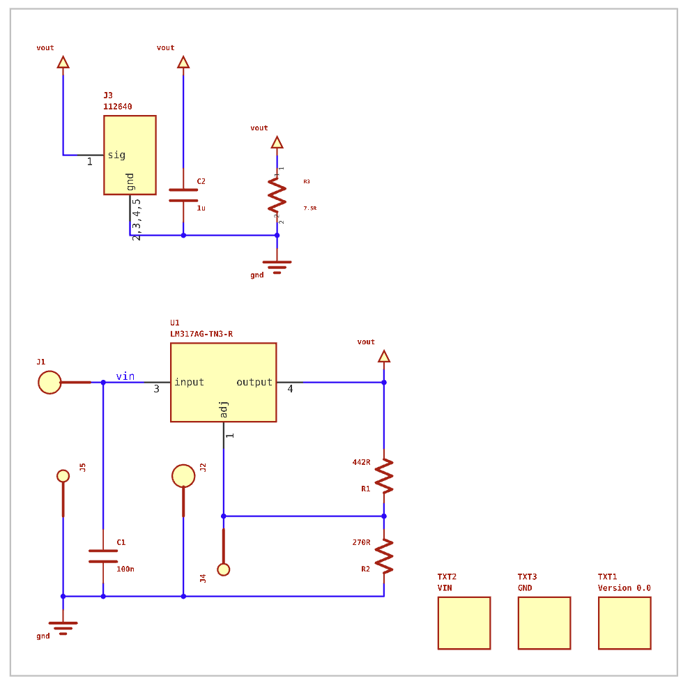
We can assign symbols to any net in JITX. Symbols for power and ground nets go a long way towards schematic organization.
4. Schematic and Layout Grouping
The #1 ticket to schematic legibility is schematic-groups. These are groups we apply as users to cluster symbols that should appear together in the schematic. JITX gives us a few ways to manage them automatically.
Schematic and Layout Groups - Inside Modules
One place where we can define a schematic group is inside of a module.
We want to always have the regulator grouped with its passives in the schematic. To do that, we can modify code inside the module definition of lm317a-regulator. Let's add the following code after the last net statement inside lm317a-regulator:
; inside pcb-module lm317a-regulator
schematic-group(self) = lm317a
layout-group(self) = lm317a
Now, all the parts in the lm317a-regulator module will be grouped together in any design we include it in. Once we add one group and recompile, every symbol belonging to an ungrouped component is automatically put into another group.
Schematic and Layout Groups - At the Top Level
Another place where we can define a schematic group is at the top level of the design.
In the top level of our design let's put our test points and the BNC connector into their own group. In the main module, put those components together in a group called test by adding this line of code at the end of my-design:
; inside pcb-module my-module
schematic-group([test-points, measure]) = test
layout-group([test-points, measure]) = test
Schematic and Layout Groups - With Other Groups
Another way to control schematic groups is by adding a component or module to an existing schematic-group.
For example, the load resistor is still grouping with the banana plug symbols. For this design, let's group it with the regulator group by adding this line of code at the end of my-design:
;inside pcb-module my-module
schematic-group(load) = schematic-group(reg)
layout-group(load) = layout-group(reg)
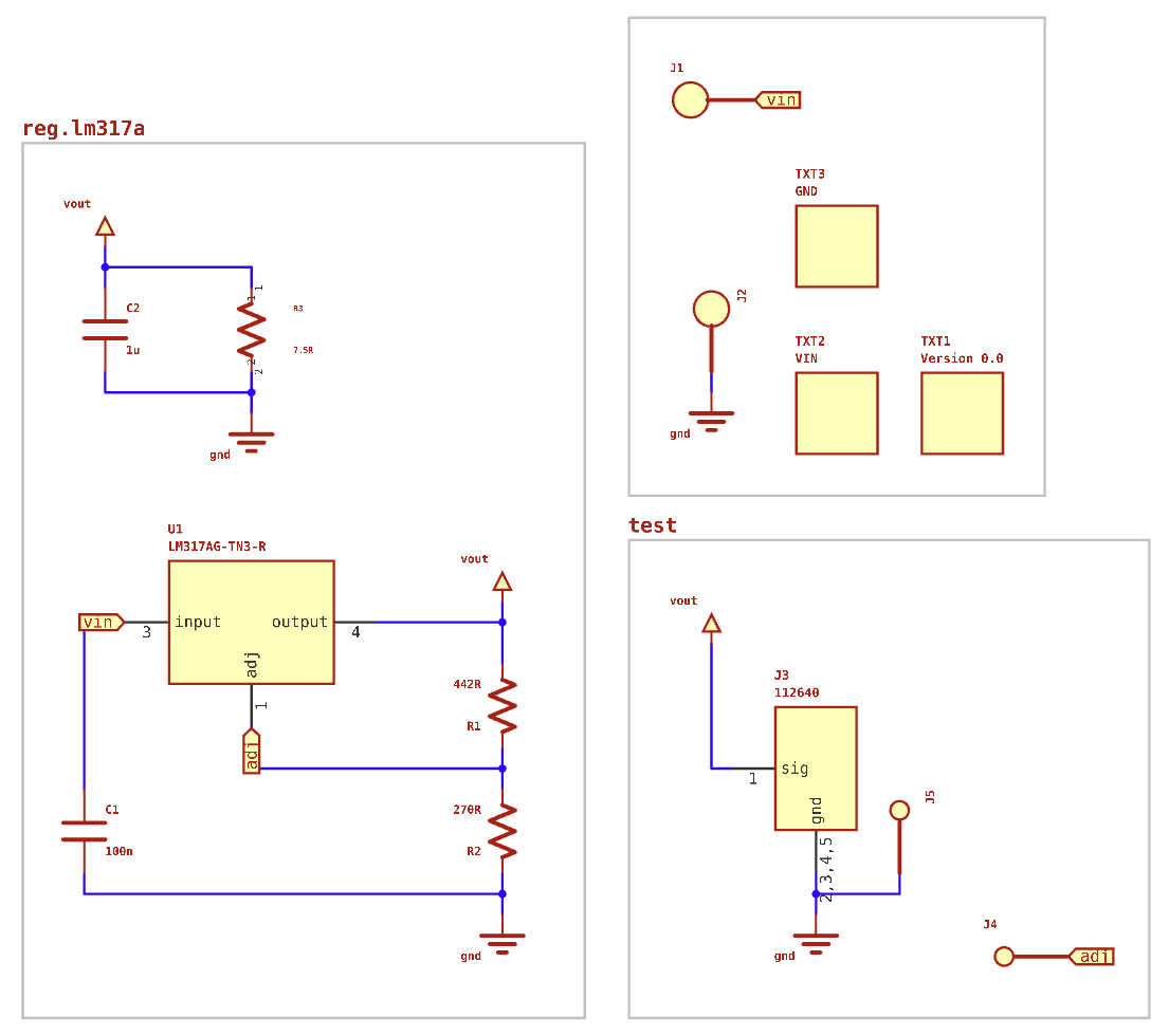
Our schematic is looking more organized and production-ready - much better!
Whenever our schematic starts getting hard to read or slow to route, it's important to apply groups to keep things organized.
Using Layout Groups in Placement
As we can see above, the schematic-groups are now part of our schematic. However, the layout-groups did not apply. By default, JITX does not use layout groups, as it can slow down placement. Since we want our layout groups to be applied during placement, we should add the following command near the bottom of main.stanza just before set-main-module:
set-use-layout-groups()
Now, JITX uses our specified layout groups when doing automatic placement:
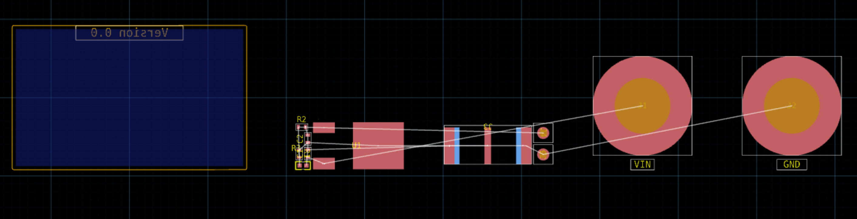
5. Using the Interactive Schematic to Organize our Design
JITX has an interactive schematic view which allows us to interact with our schematic similiarly to how you would in Altium or KiCad, but it can be done directly in VSCode. You can move components, create new sheets, and organize your design as you see fit. One major difference between JITX Schematics and classical CAD schematics is that you can't delete connections in JITX. If you want to change connectivity in a JITX design, you should do that in code. In the schematic, the focus is on legibility and organization.
Hierarchical View
If your schematic has schematic groups, then JITX automatically gives you a hierarchical view of your design. This is always on sheet 0 (the leftmost sheet in the sheet view. Here's the hierarchical group diagram for the LM317A design in this tutorial:
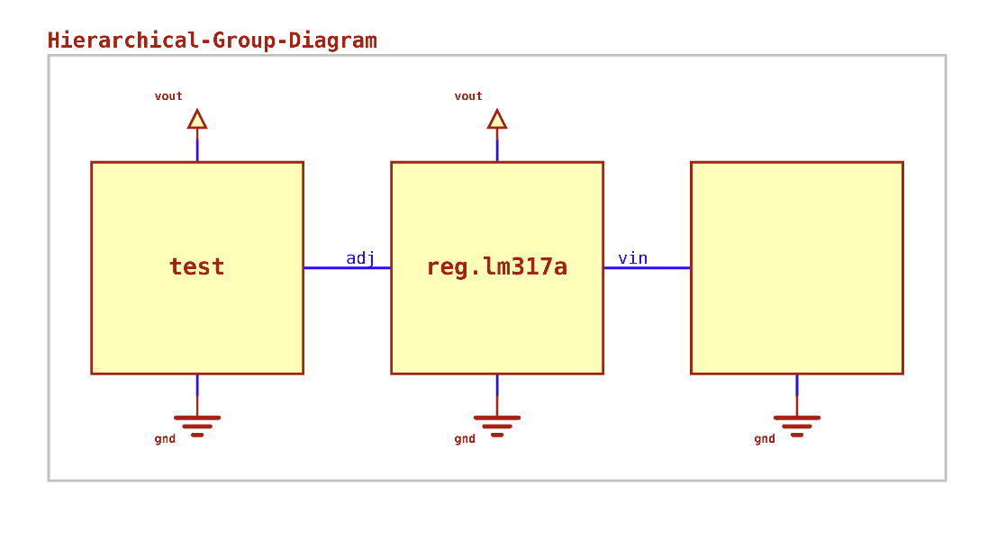
One can click on any group within this design to jump to that group. Let's click the reg.lm317a to view that submodule (which will bring us to another sheet).
Now we've jumped to that submodule directly!
Moving and Rotating Components
I might want to tighten up the schematic look a bit better. To move components, I just hover my mouse over the component, click, hold, and drag, and then release the mouse button when I want to place the component. I can also press "r" at any time to rotate the component. Here, I moved and rotated a few components:
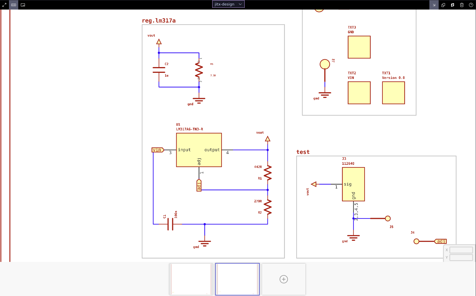
Joining Nets
We can join nets together by selecting their labels and pressing "q". Here, I joined vout and gnd from both circuits and moved components to make our submodule much cleaner and easier to parse:
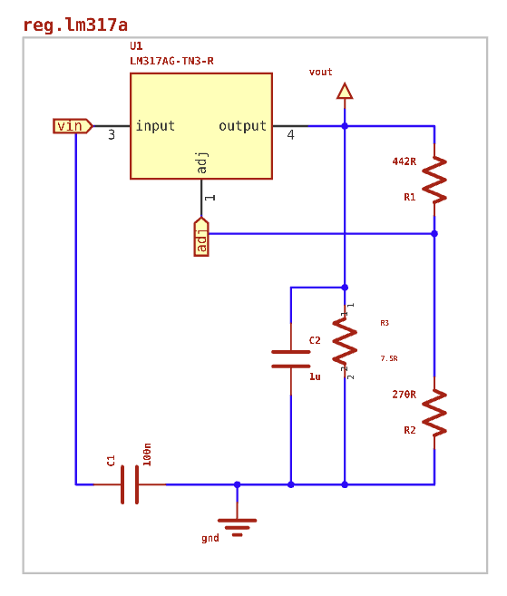
Selecting Nets
If you want to select an entire net, select any trace of that net, then press "a":
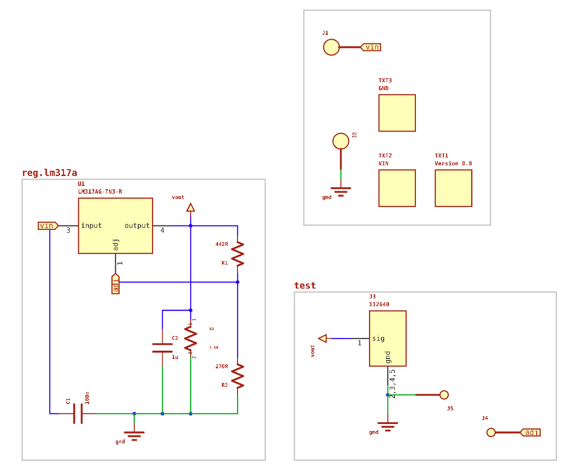
Component Info Card
If you want more information about any specific component, hover your mouse over it and press "e":
Undo/Redo
If you performed an action that you didn't want to retain, you can undo with Ctrl+z, and you can redo with Ctrl+Shift+z.
Move a Schematic Group
Schematics groups can be moved as a unit. Just place your cursor on the bounding box outline of the schematic group, click, drag and release to move it. If you want to move the schematic group to a new sheet, then press the sheet number on your keyboard while hold the schematic group, and you will jump to that sheet while still holding the schematic group.
6. Using the Physical Design to Layout our Board
First off, looking at the layout from above, it looks like our board isn't big enough. Let's go into the code and make the board-shape a bit bigger. Let's change it to:
; Define the shape/size of the board
val board-shape = RoundedRectangle(35.0, 25.0, 0.25)
Now let's recompile, and the shape of the board will change.
Placing Landpatterns
Let's place a landpattern. We can start with the banana plugs. First, hover your mouse over the banana plug and click to select it. Then click and drag your mouse to move it.
Creating Routes
Select any two or more pads at the same time (using Shift+Click) that you want to route and click the "Autoroute" button in the right corner, or press "q", and you routes will appear. Here's what it looks like if you move a few components and use "q" to autoroute a few of them.
Creating Vias
If we want to create a via, we need to enter via mode by clicking the "Via" button in the top right, or by pressing "v". Then we need to click a pad, and drag out from that pad to place a via that is routed to that pad. Here's a few vias made:
Note that you don't need to make vias for J2 and J5 as they are through-hole components. If you try to make a via on them, they don't connect.
Controlling Layers
So far, all of our routes have been on the top layer. To route on the bottom layer, we click the layers panel in the top left corner of the board view, and select the bottom layer. We can also go through layers by pressing "s" or "w". In this case, we don't need to route on any other layer as our vias are connected to the ground plane in the inner layers.
Layout Complete
You've now learned how to use the JITX schematic and board views to organize, layout, and route your PCB.
Before moving on, let's clear our work so it's fresh for the next quickstarts. To do so, just delete the contents inside the designs directory in the VSCode File Explorer.
Next step
Continue with the Quickstart: Check a Design to learn how to add checks that make sure this design will actually work when we get the hardware back.
Completed Code for the Quickstart: Organize a Design Tutorial
Also the starting code for the Quickstart: Circuit Generators Tutorial
#use-added-syntax(jitx)
defpackage main :
import core
import jitx
import jitx/commands
import ocdb/utils/generic-components
import helpers
; Define the shape/size of the board
val board-shape = RoundedRectangle(35.0, 25.0, 0.25)
; Setup the board
defn setup-board () :
set-board(ocdb/utils/defaults/default-board(ocdb/manufacturers/stackups/jlcpcb-jlc2313, board-shape))
set-rules(ocdb/manufacturers/rules/jlcpcb-rules)
pcb-module lm317a-regulator (output-voltage:Toleranced) :
pin vin
pin vout
pin gnd
pin adj
inst lm317a : ocdb/components/unisonic/LM317A/component
net (vin lm317a.input)
net (vout lm317a.output)
cap-strap(lm317a.input, gnd, 0.1e-6)
cap-strap(lm317a.output, gnd, 1.0e-6)
inst output-voltage-divider : ocdb/modules/passive-circuits/voltage-divider(source-voltage = in-voltage, divider-output = adj-voltage, current = current) where :
val in-voltage = output-voltage
val adj-voltage = tol%(1.25, 15.0)
val current = 5.0e-3
; inside pcb-module lm317a-regulator
schematic-group(self) = lm317a
layout-group(self) = lm317a
net (output-voltage-divider.in lm317a.output)
net (output-voltage-divider.out lm317a.adj adj)
net (output-voltage-divider.lo gnd)
; Module to run as a design
pcb-module my-design :
val target-voltage = tol%(3.3, 10.0)
inst reg : lm317a-regulator(target-voltage)
; Write the board version on silkscreen
inst version-label : ocdb/artwork/board-text/version-silkscreen("Version 0.0")
place(version-label) at loc(0.0, height(board-shape) / 2.0 - 1.0) on Bottom
inst source : banana-plug-module() ; shortcut to instantiate and place two `banana-plug`s plus the electrical support
net gnd (reg.gnd, source.power.gnd)
net vin (reg.vin, source.power.vdd)
inst measure : bnc-connector()
net vout (reg.vout, measure.sig)
net (gnd, measure.gnd)
val test-points = add-testpoint([reg.adj, gnd])
val target-current = 450.0e-3
val target-load = closest-std-val(typ-value(target-voltage) / target-current, 5.0)
inst load : chip-resistor(["resistance" => target-load, "min-rated-power" => typ-value(target-voltage) * target-current * 2.0 ])
net (load.p[1], reg.vout)
net (load.p[2], gnd)
symbol(gnd) = ocdb/utils/symbols/ground-sym ; has to be placed after the definition of the net itself
symbol(vout) = ocdb/utils/symbols/supply-sym ; has to be placed after the definition of the net itself
; add a ground plane
geom(gnd) :
copper-pour(LayerIndex(1), isolate = 0.1, rank = 1, orphans = true) = Rectangle(width(board-shape) - 1.0, height(board-shape) - 1.0)
; add a net class for power nets
val power-net-class = NetClass(`Power, [`min-trace => 0.381])
property(gnd.net-class) = power-net-class
property(vout.net-class) = power-net-class
property(vin.net-class) = power-net-class
; inside pcb-module my-module
schematic-group([test-points, measure]) = test
layout-group([test-points, measure]) = test
;inside pcb-module my-module
schematic-group(load) = schematic-group(reg)
layout-group(load) = layout-group(reg)
; Run the code
set-current-design("jitx-design") ;set the directory where the generated output will be placed
setup-board()
set-use-layout-groups()
set-main-module(my-design)
; Use a helper function from helpers.stanza (use any helper function here)
; run-check-on-design(my-design)
; View the results
view-board()
view-schematic()
view-design-explorer()
Quickstart: Circuit Generators
In this tutorial, we'll update the LM317A regulator design from the Quickstart: Your First JITX Design to use a circuit generator when choosing its voltage divider.
NOTE: This Quickstart begins where Quickstart: Organize a Schematic finishes. For your reference, the starting code for the file
main.stanzaand the finished code for this Quickstart tutorial are available.
Tutorial - Circuit Generators
In conventional CAD, we're used to designing every subcircuit/submodule invidivually by hand, separately computing values every time. Often, submodules are nearly identical to each other, but with different values. In these circumstances, we can use circuit generators, which are just functions that return pcb-modules (circuits), to design a circuit one time using input parameters, and then use that design for many different parameters.
You can imagine using circuit generators for all kinds of similar subcircuits:
- voltage divider
- LDO module
- indicator LED with ballast resistor and pulldown
- more
JITX and OCDB have a number of circuit generators built in that you can call. Also, you can define any circuit generator you need.
In this tutorial, we'll use the built-in voltage-divider circuit generator to improve our LM317A implementation.
NOTE: Some of the code block changes rely on later changes to work. If the project doesn't build at some point throughout the tutorial - don't worry. Keep working through the tutorial, and everything should build after making the subsequent changes.
1. Module Properties - Datasheet Values of the LM317A in Code
We're going to need to query electrical properties from the LM317A component in order to write our circuit generator (you can Ctrl+Click in VS Code to go to definition of this component and see which properties are modeled). For example, a property that we will use later in this guide is called property(lm317a.adj-current) which fetches the property named adj-current from the module instance named lm317a. Here is a list of the properties associated with the LM317A, which you can find by looking at the source code of the LM317A:
(Don't copy-paste this block):
property(self.rated-temperature) = min-max(-40.0 85.0) ; rated temperature range (in C) for this component
property(self.reference-voltage) = min-typ-max(1.20, 1.25, 1.3) ; reference voltage range in Toleranced type from the datasheet
property(self.minimum-load) = 4.5e-3 ; minimum current (A) for proper operation of the regulator
property(self.adj-current) = 50.0e-6 ; expected current (A) for the voltage feedback divider
property(self.max-current) = 1.5 ; maximum current (A) that the regulator can supply to the load
eval-when has-property?(self.input.voltage) and has-property?(self.output.voltage) :
val v-out = typ-value(property(self.output.voltage))
; Set voltage limits based on figure from page 5.
property(self.input.power-pin) = ocdb/utils/property-structs/PowerPin(min-max(v-out + 5.0, v-out + 40.0)) ; this property is only set when the input has a valid `voltage` property
2. Adding a Circuit Generator - A Better Voltage Divider
The voltage divider in lm317a-regulator must keep the reference voltage within the specified range given by output-voltage:Toleranced. The voltage divider solver accepts Toleranced arguments and can solve this problem for us. Calculations that we usually do in spreadsheets or comments on a schematic can be code in JITX, so now we're going to do some math to design this circuit.
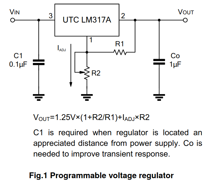
First off a sanity check - the reference voltage variance on this LM317A can be a problem (only guaranteed to be 4% accurate). Let's check that the accuracy of this regulator doesn't cause the design to be out of specification. To do so, let's add the following codeblock near the bottom of our lm317a-regulator pcb-module (but above the grouping statements).
; How much variability can we expect from the regulator alone?
val refVoltage = property(lm317a.reference-voltage)
val inherent-variance = tol+%(refVoltage)
if inherent-variance > tol+%(output-voltage):
fatal("Target design accuracy infeasible with LM317A %_ > %_" % [inherent-variance tol+%(output-voltage)])
We can then budget the allowable error for the voltage divider by adding the following codeblock below the code we just added:
; Budget variability for the voltage divider
val target-variance = tol+%(output-voltage) - inherent-variance
Finally we need to compensate for the current that the adj pin can source. We choose 5mA of voltage divider current to reduce the overall perturbation, then estimate how to update the set point to compensate.
Add the following codeblock below the code we just added:
; 5mA of voltage-divider current to compensate for regulator adj current
val divider-current = 5.0e-3
val adj-current = property(lm317a.adj-current) ; retrieve the property from the component definition
; Estimate offset voltage caused by current sourced from adj pin
val est-v-adj-offset = (typ-value(output-voltage) - typ-value(refVoltage)) / divider-current * adj-current
We feed these parameters into the voltage divider solver, which will find a combination of triply-sourceable resistors that produce a voltage within the specified range (including effects of temperature, TCR, manufacturer tolerance, etc.). Notice that we leave off specifying the tolerance of resistors to use in the divider and let the solver find the optimal tolerance range. Remove the old voltage-divider definition block from the lm317a-regulator and paste the following code at the bottom of the lm317a-regulator block:
inst output-voltage-divider : ocdb/modules/passive-circuits/voltage-divider(source-voltage = high-voltage, divider-output = adj-voltage, current = current) where :
val high-voltage = tol%(center-value(output-voltage) - est-v-adj-offset, 0.0)
val adj-voltage = tol%(typ-value(refVoltage),target-variance)
val current = divider-current
Make sure you go back and delete the previous definition of output-voltage-divider - we don't need that anymore as we have a new definition.
You can now build the design (Ctrl + Enter). Nice!
Next Step
Add and run checks on this design by following Quickstart: Check a Design.
Completed code for the Quickstart: Circuit Generators Tutorial
Also the starting code for the Quickstart: Check a Design Tutorial
#use-added-syntax(jitx)
defpackage main :
import core
import jitx
import jitx/commands
import ocdb/utils/generic-components
import helpers
; Define the shape/size of the board
val board-shape = RoundedRectangle(30.0, 18.5, 0.25)
; Setup the board
defn setup-board () :
set-board(ocdb/utils/defaults/default-board(ocdb/manufacturers/stackups/jlcpcb-jlc2313, board-shape))
set-rules(ocdb/manufacturers/rules/jlcpcb-rules)
pcb-module lm317a-regulator (output-voltage:Toleranced) :
pin vin
pin vout
pin gnd
pin adj
inst lm317a : ocdb/components/unisonic/LM317A/component
net (vin lm317a.input)
net (vout lm317a.output)
cap-strap(lm317a.input, gnd, 0.1e-6)
cap-strap(lm317a.output, gnd, 1.0e-6)
; How much variability can we expect from the regulator alone?
val refVoltage = property(lm317a.reference-voltage)
val inherent-variance = tol+%(refVoltage)
if inherent-variance > tol+%(output-voltage):
fatal("Target design accuracy infeasible with LM317A %_ > %_" % [inherent-variance tol+%(output-voltage)])
; Budget variability for the voltage divider
val target-variance = tol+%(output-voltage) - inherent-variance
; 5mA of voltage-divider current to compensate for regulator adj current
val divider-current = 5.0e-3
val adj-current = property(lm317a.adj-current) ; retrieve the property from the component definition
; Estimate offset voltage caused by current sourced from adj pin
val est-v-adj-offset = (typ-value(output-voltage) - typ-value(refVoltage)) / divider-current * adj-current
inst output-voltage-divider : ocdb/modules/passive-circuits/voltage-divider(source-voltage = high-voltage, divider-output = adj-voltage, current = current) where :
val high-voltage = tol%(center-value(output-voltage) - est-v-adj-offset, 0.0)
val adj-voltage = tol%(typ-value(refVoltage),target-variance)
val current = divider-current
; inside pcb-module lm317a-regulator
schematic-group(self) = lm317a
layout-group(self) = lm317a
net (output-voltage-divider.in lm317a.output)
net (output-voltage-divider.out lm317a.adj adj)
net (output-voltage-divider.lo gnd)
; Module to run as a design
pcb-module my-design :
val target-voltage = tol%(3.3, 10.0)
inst reg : lm317a-regulator(target-voltage)
; Write the board version on silkscreen
inst version-label : ocdb/artwork/board-text/version-silkscreen("Version 0.0")
place(version-label) at loc(0.0, height(board-shape) / 2.0 - 1.0) on Bottom
inst source : banana-plug-module() ; shortcut to instantiate and place two `banana-plug`s plus the electrical support
net gnd (reg.gnd, source.power.gnd)
net vin (reg.vin, source.power.vdd)
inst measure : bnc-connector()
net vout (reg.vout, measure.sig)
net (gnd, measure.gnd)
val test-points = add-testpoint([reg.adj, gnd])
val target-current = 450.0e-3
val target-load = closest-std-val(typ-value(target-voltage) / target-current, 5.0)
inst load : chip-resistor(["resistance" => target-load, "min-rated-power" => typ-value(target-voltage) * target-current * 2.0 ])
net (load.p[1], reg.vout)
net (load.p[2], gnd)
symbol(gnd) = ocdb/utils/symbols/ground-sym ; has to be placed after the definition of the net itself
symbol(vout) = ocdb/utils/symbols/supply-sym ; has to be placed after the definition of the net itself
; add a ground plane
geom(gnd) :
copper-pour(LayerIndex(1), isolate = 0.1, rank = 1, orphans = true) = Rectangle(width(board-shape) - 1.0, height(board-shape) - 1.0)
; add a net class for power nets
val power-net-class = NetClass(`Power, [`min-trace => 0.381])
property(gnd.net-class) = power-net-class
property(vout.net-class) = power-net-class
property(vin.net-class) = power-net-class
; inside pcb-module my-module
layout-group([test-points, measure]) = test
;inside pcb-module my-module
schematic-group(load) = schematic-group(reg)
layout-group(load) = layout-group(reg)
; Run the code
set-current-design("jitx-design") ;set the directory where the generated output will be placed
setup-board()
set-main-module(my-design)
; Use a helper function from helpers.stanza (use any helper function here)
; run-check-on-design(my-design)
; View the results
view-board()
view-schematic()
view-design-explorer()
Quickstart: Check a Design
In this tutorial, we'll add checks to the regulator design from the Quickstart: Your First JITX Design. These checks add certainty that our circuit will function as expected, and make design work in JITX more reusable. It's easier to use someone else's circuit when that circuit can check itself for correctness.
NOTE: This Quickstart begins where Quickstart: Circuit Generators finishes. For your reference, the starting code for the file
main.stanzaand the finished code for this Quickstart tutorial are available.
Tutorial - Checks
In conventional CAD, we're used to running "Design Rules Checks" (DRC) and "Electrical Rules Checks" (ERC) to ensure that our schematic and board are logical and manufacturable. JITX supports those checks, but it also supports a wide range of checks that go far past traditional DRC and ERC.
You can run built-in checks that check:
- voltage input/output correctness
- pull-ups/pull-downs
- rated temperature compliance
- more
JITX also supports writing your own checks. You can define any requirement you want about your components or modules in code, and then write a check to ensure that requirement is met.
In this tutorial, we'll ensure validity of our implementation of the LM317A module by writing checks for it.
NOTE: Some of the code block changes rely on later changes to work. If the project doesn't build at some point throughout the tutorial - don't worry. Keep working through the tutorial, and everything should build after making the subsequent changes.
1. Adding a Custom Check
As discussed above, we can write custom checks that check for just about anything.
For example, if we wanted to make sure that the component that we imported always has a rated-temperature property defined, we could do so by writing the following custom check:
pcb-check check-rated-temperature (component:JITXObject):
#CHECK(
name = "Has Rated Temperature"
description = "Check that a component has a rated-temperature property"
condition = has-property?(component.rated-temperature),
category = "Component Data"
subcheck-description = "Check that %_ has a defined rated-temperature" % [ref(component)],
pass-message = "%_ has a property for rated-temperature of %_" % [ref(component) property(component.rated-temperature)],
info-message = "%_ does not have a rated-temperature property attached" % [ref(component)],
locators = [instance-definition(component)]
)
And then running it on the LM317A by adding the following codeblock to the lm317a pcb-module definition:
check check-rated-temperature(lm317a)
Compile the design and run run-check-on-design(main-module) in the JITX Shell. Then, open the "JITX: Check Report" panel, and you can see that our custom check ran successfully.
2. Adding a Built-in Check
We handed off the voltage divider design work to a solver. Let's add a check to the lm317a-regulator module so we can trust the resulting output voltage. We now have two real resistors that we can query for properties to determine the actual operating point of the circuit. The Toleranced type does interval arithmetic for us, so the range of operation can be directly calculated. Let's add that code in the lm317a-regulator below the output-voltage-divider:
; Calculate the actual offset now that we know the optimized value of the resistors
val true-adj-offset = adj-current * (property(output-voltage-divider.r-lo.resistance) as Double)
val vref = property(output-voltage-divider.output-voltage)
; Calculate the possible min and max values for the output voltage
val out = refVoltage * typ(center-value(output-voltage)) / vref + typ(true-adj-offset)
And at last, we use a check from ocdb/utils/checks to make sure that the expected output voltage is within the range specified by adding the following codeblock starting inside lm317a-regulator, near the end but above the net statements:
; Make sure that the voltage specification is met
check ocdb/utils/checks/within?(output-voltage, out)
Run the above with Ctrl + Enter. Then, in the JITX Shell, type run-check-on-design(my-design) to run the check we added to the LM317A circuit.
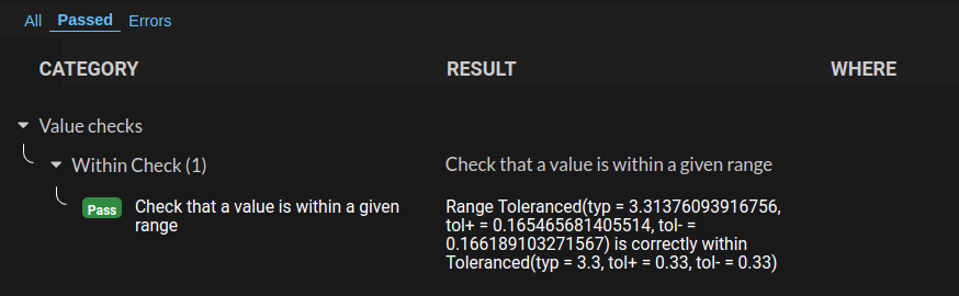
This check will run every time someone using this circuit analyzes their design, so we don't have to be present for every design review on this LM317A.
3. Adding Many Built-in Checks
We can invoke many checks automatically by adding this line of code to the bottom of our top level pcb-module (my-design).
ocdb/utils/checks/check-design(self)
The check-design function in ocdb/utils/checks scrubs through our design looking for properties that identify passives, voltage rails, power pins and digital-io. We can provide these checks with more information by annotating the voltages we know as properties on nets by adding the following codeblock near the end of my-design:
property(gnd.voltage) = typ(0.0)
property(vout.voltage) = target-voltage
property(vin.voltage) = typ(10.0)
Here, the gnd net is 0.0V, vout is our target voltage, and we specify vin to be 10.0V. Based on that, we see new check results (along with our custom check).
Then Ctrl + Enter to re-build, and re-run run-check-on-design(my-design) to run a variety of checks on our design.
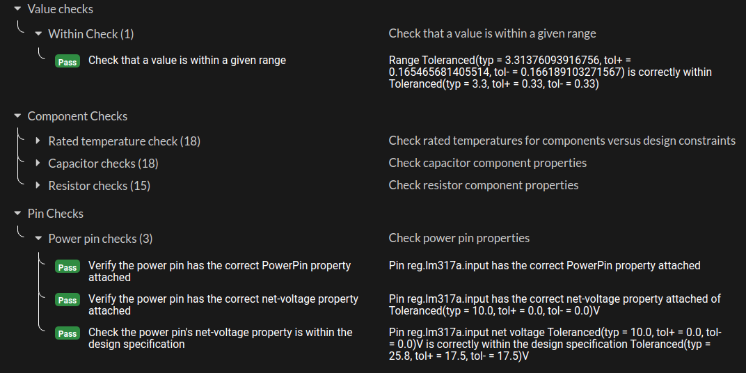
We have derating calculations for all of our passives, manufacturability checks on landpatterns, and a voltage check on the input pin of the regulator.
Note that to pass the derating checks we had to specify the minimum voltage of the capacitors in the LM317A circuit:
cap-strap(vin, gnd, ["capacitance" => 0.1e-6 "min-rated-voltage" => 25.0])
cap-strap(vout, gnd, ["capacitance" => 1.0e-6 "min-rated-voltage" => 25.0])
The checking system does not catch every possible error (yet), but it can significantly reduce the risk of our design process by checking the simple stuff. Just adding the properties of power pins and digital-io to JITX as we read datasheets will save quite a few bad boards.
Next Step
Start working with existing design data by importing an Altium design.
Final Code for the Quickstart: Check a design Tutorial
#use-added-syntax(jitx)
defpackage main :
import core
import jitx
import jitx/commands
import ocdb/utils/generic-components
import helpers
; Define the shape/size of the board
val board-shape = RoundedRectangle(30.0, 18.5, 0.25)
; Setup the board
defn setup-board () :
set-board(ocdb/utils/defaults/default-board(ocdb/manufacturers/stackups/jlcpcb-jlc2313, board-shape))
set-rules(ocdb/manufacturers/rules/jlcpcb-rules)
pcb-check check-rated-temperature (component:JITXObject):
#CHECK(
name = "Has Rated Temperature"
description = "Check that a component has a rated-temperature property"
condition = has-property?(component.rated-temperature),
category = "Component Data"
subcheck-description = "Check that %_ has a defined rated-temperature" % [ref(component)],
pass-message = "%_ has a property for rated-temperature of %_" % [ref(component) property(component.rated-temperature)],
info-message = "%_ does not have a rated-temperature property attached" % [ref(component)],
locators = [instance-definition(component)]
)
pcb-module lm317a-regulator (output-voltage:Toleranced) :
pin vin
pin vout
pin gnd
pin adj
inst lm317a : ocdb/components/unisonic/LM317A/component
check check-rated-temperature(lm317a)
net (vin lm317a.input)
net (vout lm317a.output)
cap-strap(lm317a.input, gnd, 0.1e-6)
cap-strap(lm317a.output, gnd, 1.0e-6)
; inside pcb-module lm317a-regulator
schematic-group(self) = lm317a
layout-group(self) = lm317a
; How much variability can we expect from the regulator alone?
val refVoltage = property(lm317a.reference-voltage)
val inherent-variance = tol+%(refVoltage)
if inherent-variance > tol+%(output-voltage):
fatal("Target design accuracy infeasible with LM317A %_ > %_" % [inherent-variance tol+%(output-voltage)])
; Budget variability for the voltage divider
val target-variance = tol+%(output-voltage) - inherent-variance
; 5mA of voltage-divider current to compensate for regulator adj current
val divider-current = 5.0e-3
val adj-current = property(lm317a.adj-current) ; retrieve the property from the component definition
; Estimate offset voltage caused by current sourced from adj pin
val est-v-adj-offset = (typ-value(output-voltage) - typ-value(refVoltage)) / divider-current * adj-current
inst output-voltage-divider : ocdb/modules/passive-circuits/voltage-divider(source-voltage = high-voltage, divider-output = adj-voltage, current = current) where :
val high-voltage = tol%(center-value(output-voltage) - est-v-adj-offset, 0.0)
val adj-voltage = tol%(typ-value(refVoltage),target-variance)
val current = divider-current
; Calculate the actual offset now that we know the optimized value of the resistors
val true-adj-offset = adj-current * (property(output-voltage-divider.r-lo.resistance) as Double)
val vref = property(output-voltage-divider.output-voltage)
; Calculate the possible min and max values for the output voltage
val out = refVoltage * typ(center-value(output-voltage)) / vref + typ(true-adj-offset)
; Make sure that the voltage specification is met
check ocdb/utils/checks/within?(output-voltage, out)
net (output-voltage-divider.in lm317a.output)
net (output-voltage-divider.out lm317a.adj adj)
net (output-voltage-divider.lo gnd)
; Module to run as a design
pcb-module my-design :
val target-voltage = tol%(3.3, 10.0)
inst reg : lm317a-regulator(target-voltage)
; Write the board version on silkscreen
inst version-label : ocdb/artwork/board-text/version-silkscreen("Version 0.0")
place(version-label) at loc(0.0, height(board-shape) / 2.0 - 1.0) on Bottom
inst source : banana-plug-module() ; shortcut to instantiate and place two `banana-plug`s plus the electrical support
net gnd (reg.gnd, source.power.gnd)
net vin (reg.vin, source.power.vdd)
inst measure : bnc-connector()
net vout (reg.vout, measure.sig)
net (gnd, measure.gnd)
val test-points = add-testpoint([reg.adj, gnd])
val target-current = 450.0e-3
val target-load = closest-std-val(typ-value(target-voltage) / target-current, 5.0)
inst load : chip-resistor(["resistance" => target-load, "min-rated-power" => typ-value(target-voltage) * target-current * 2.0 ])
net (load.p[1], reg.vout)
net (load.p[2], gnd)
symbol(gnd) = ocdb/utils/symbols/ground-sym ; has to be placed after the definition of the net itself
symbol(vout) = ocdb/utils/symbols/supply-sym ; has to be placed after the definition of the net itself
; add a ground plane
geom(gnd) :
copper-pour(LayerIndex(1), isolate = 0.1, rank = 1, orphans = true) = Rectangle(width(board-shape) - 1.0, height(board-shape) - 1.0)
; add a net class for power nets
val power-net-class = NetClass(`Power, [`min-trace => 0.381])
property(gnd.net-class) = power-net-class
property(vout.net-class) = power-net-class
property(vin.net-class) = power-net-class
; inside pcb-module my-module
layout-group([test-points, measure]) = test
;inside pcb-module my-module
schematic-group(load) = schematic-group(reg)
layout-group(load) = layout-group(reg)
property(gnd.voltage) = typ(0.0)
property(vout.voltage) = target-voltage
property(vin.voltage) = typ(10.0)
; ocdb/utils/checks/check-design(self)
; Run the code
set-current-design("jitx-design") ;set the directory where the generated output will be placed
setup-board()
set-main-module(my-design)
; Use a helper function from helpers.stanza (use any helper function here)
; run-check-on-design(my-design)
; View the results
view-board()
view-schematic()
view-design-explorer()
Learn JITX
This set of docs is a sequence that builds from zero knowledge of JITX through familiarity of all the commonly used syntax and design patterns.
Components and nets
In the last section we created a design with a single component. This section will show you how define components starting from scratch, and connect their pins with nets.
We typically use components to model discrete devices (e.g. resistors, capacitors, op-amps, FPGAs,etc ..). In practice, each component definition captures a whole family of devices. For example, every fuse in this datasheet would be captured by a single component model.
We create a component using the pcb-component statement and add pins to it using the pin and port statements. Here are definitions for three components needed for our design, a photodiode, an op-amp, and a pin-header.
pcb-component photodiode :
pin a
pin c
pcb-component op-amp :
pin in+
pin in-
pin out
pin v+
pin v-
pcb-component three-pin-header :
port p : pin[3]
This code snippet:
- Defines a new component named
photodiodewith two pins namedaandc - Defines a new component named
op-ampwith five pins namedin+,in-,out,v+, andv- - Defines a new component named
three-pin-headerwith a port namedp, that has three pins. The pins in this port have the namesp[0]p[1]andp[2].
We can add these components to our design using the inst statement (short for instantiate). Let's create a small circuit connecting the photodiode to the op-amp, and pins associated with power to the connector.
pcb-module my-design :
inst d : photodiode
inst opa : op-amp
inst connector : three-pin-header
; Set up power connections
net GND (opa.v- connector.p[0])
public net VDD (opa.v+ connector.p[1])
; Connect op-amp
net (d.c opa.in-)
net (GND opa.in+ d.a)
To break this down, we first instantiate our components:
inst d : photodiode
inst opa : op-amp
inst connector : three-pin-header
- One instance of
op-ampnamedopa - One instance of
photodiodenamedd - One instance of
three-pin-headernamedconnector
Then we create a net named GND that connects the negative supply on the op-amp, and the first pin on the pin-header :
net GND (opa.v- connector.p[0])
This statement creates a new net named GND. Every pin inside the parentheses will be added to this GND net. We named the instance of our connector connector and we can access its pins using the . operator, so the name of the first pin of the connector is j.p[0].
Similarly this statement creates the VDD net, and connects the positive op-amp supply pin and the second pin on the connector :
public net VDD (opa.v+ connector.p[1])
Then we connect the cathode of the photodiode to the inverting input of the op-amp :
net (d.c opa.in-)
We could give that net a name but it's optional. Nets that we don't name get auto-generated names later.
Finally, we connect the non-inverting op-amp input and the anode of the photodiode to ground :
net (GND opa.in+ d.a)
Notice that we are using the name GND to add these other pins to the GND net.
Example code for this design is here. Because we didn't add symbols to our components (yet) we can't generate a schematic to see what our code is doing. Instead, we used some introspection to print out the members of the VDD net (which we made public for that purpose).
This section showed you how to create new components, instantiate them in a design, and connect them up using the net statement. However we're still missing some information in the components. There's no symbol or land pattern or sourcing information (the reference has a complete list of component statements). And so even though this is a valid design in JITX, we wouldn't be able to create a schematic (because there are no symbols), or a layout (because there are no land patterns). We will see how to add that information in the next section.
#use-added-syntax(jitx)
defpackage first-design :
import core
import jitx
import jitx/commands
pcb-component photodiode :
pin a
pin c
pcb-component op-amp :
pin in+
pin in-
pin out
pin v+
pin v-
pcb-component three-pin-header :
port p : pin[3]
pcb-module my-design :
inst d : photodiode
inst opa : op-amp
inst connector : three-pin-header
; Set up power connections
net GND (opa.v- connector.p[0])
public net VDD (opa.v+ connector.p[1])
; Connect op-amp
net (d.c opa.in-)
net (GND opa.in+ d.a)
for p in refs(my-design.VDD) do :
println(ref(p))
Land patterns and symbols
We can use JITX to generate a complete CAD package from our generator code. To generate a board design from our generator, each component we include needs to have an associated land pattern. To generate a schematic, each component also needs to have an associated symbol.
This section shows you how to work with low-level land pattern and symbol definitions. In practice we generate pads, land patterns, and symbols programmatically (as you will see in the next section), but this section will give you the foundations to understand what it being generated. Example code for this section is here.
Land Patterns
We use land patterns to model the geometry that attaches a component to a board. We create a land pattern using the pcb-landpattern statement and add pads to it using the pad statement. Let's define a land pattern for our three-pin-header from the previous section.
Let's first define a pad named round-pth-pad. This is a plated through-hole pad, the copper shape is a circle with an 0.8mm radius and the hole has an 0.5mm radius. We define SolderMask layer of the same shape top and bottom to go along with the copper pad.
pcb-pad round-pth-pad :
type = TH
shape = Circle(0.8)
layer(Cutout()) = Circle(0.5)
layer(SolderMask(Top)) = Circle(0.8)
layer(SolderMask(Bottom)) = Circle(0.8)
Next we define a land pattern for our pin-header that includes three of these round-pth-pad pads.
pcb-landpattern pin-header-landpattern :
pad p[1] : round-pth-pad at loc(-2.54, 0.0)
pad p[2] : round-pth-pad at loc(0.0, 0.0)
pad p[3] : round-pth-pad at loc(2.54, 0.0)
layer(Courtyard(Top)) = Rectangle(6.6, 1.6)
layer(Silkscreen("values", Top)) = Text(">REF", 0.7, C, loc(0.0, -1.2))
pad p[1] : round-pth-pad at loc(-2.54, 0.0) translates to 'create a pad named p[1] of type round-pth-pad, and place it at location x = -2.54mm, y = 0.0mm'.
Notice that we started our pad numbers at 1 (instead of 0) so they would more closely match a real component. We also define a courtyard to define the extents of the land pattern, and place a reference designator on the top silkscreen layer.
Here is the resulting geometry:

Finally we associate pin-header-landpattern with our three-pin-header component from the previous section:
pcb-component three-pin-header :
port p : pin[[1 2 3]]
landpattern = pin-header-landpattern(p[1] => pin-header-landpattern.p[1]
p[2] => pin-header-landpattern.p[2]
p[3] => pin-header-landpattern.p[3])
Notice that we updated to port definition to have pins p[1] p[2] and p[3] to match the land pattern (instead of starting at p[0]).
landpattern = pin-header-landpattern(p[1] => pin-header-landpattern.p[1] translates to:
- The land pattern associated with
three-pin-headerispin-header-landpattern - Pin
p[1]on the component maps to padp[1]onpin-header-landpattern.p[2]maps top[2],p[3]top[3].
So a component definition includes a reference to a land pattern, as well as a mapping that connects component ports to land pattern pads. When we instantiate a component, we can only connect to the components ports -- not the pads on the land pattern.
Symbols
Lastly, we need to define a symbol for our pin-header and associate it with our component. Here is a symbol definition for our header:
pcb-symbol pin-header-symbol :
layer("foreground") = Rectangle(2.54, 7.62, loc(-1.27, 0.0))
for i in 0 to 3 do :
pin p[(i + 1)] at Point(-2.54, (2.54 - (to-double(i) * 2.54))) with :
direction = Left
length = 2.54
number-size = 0.762
name-size = 0.762
layer("reference") = Text(">REF", 0.7056, W, loc(-2.54, 4.2))
preferred-orientation = PreferRotation([0])
First we add a graphic rectangle to our symbol:
layer("foreground") = Rectangle(2.54, 7.62, loc(-1.27, 0.0))
Then we use a for loop to place three pins on our symbol. The pin statements create connection points on the schematic. In the for loop, when i = 0, this snippet
pin p[(i + 1)] at Point(-2.54, (2.54 - (to-double(i) * 2.54))) with :
direction = Left
length = 2.54
number-size = 0.762
name-size = 0.762
Creates a pin named p[1] and places it at x = 2.54mm, and y = 2.54mm, sets the direction of the pin to face the left side, sets the length of the pin, and sets font sizes for the labels. To export to CAD correctly, we must use a 2.54mm grid for placing symbol pins. Graphics can be anywhere, but the pins have to be on that 2.54mm grid to be compatible with traditional CAD tools.
This line: layer("reference") = Text(">REF", 0.7056, W, loc(-2.54, 4.2)) sizes and places text for the reference designator. And finally we don't want to allow the schematic drawing algorithms to rotate this symbol, so we lock it in with preferred-orientation = PreferRotation([0]).
And this is how our pin-header-symbol looks:
Finally we associate pin-header-symbol with our component, and map the component pins to the symbol pins.
pcb-component three-pin-header :
port p : pin[[1 2 3]]
landpattern = pin-header-landpattern(p[1] => pin-header-landpattern.p[1]
p[2] => pin-header-landpattern.p[2]
p[3] => pin-header-landpattern.p[3])
symbol = pin-header-symbol(p[1] => pin-header-symbol.p[1]
p[2] => pin-header-symbol.p[2]
p[3] => pin-header-symbol.p[3])
reference-prefix = "J"
We also set the reference prefix of this component to be "J" (JITX defaults to "U" if the reference prefix is unspecified).
More examples
We're going to add land patterns and symbols for our op-amp and photodiode as well, but take the more usual approach of drawing on some pre-written functions to generate the symbols and land patterns. The Open Components Database (OCDB), is a library of component models, reusable circuits, example designs, and utilities to make it easy to build new designs using JITX. We're going to import symbol and land pattern generators from OCDB to do some work for us.
Here is example code for this section. (You can run this generator using the instructions in Your first JITX design). In the front matter of that program you can see the new import statements
import ocdb/utils/symbols
import ocdb/utils/box-symbol
import ocdb/utils/landpatterns
import ocdb/utils/defaults
Here is the model for our photodiode:
pcb-pad rect-smd-pad :
type = SMD
val pad-shape = Rectangle(0.75, 1.0)
shape = pad-shape
layer(SolderMask(Top)) = pad-shape
layer(Paste(Top)) = pad-shape
pcb-landpattern polarized-chip-landpattern :
pad a : rect-smd-pad at loc(1.0, 0.0)
pad c : rect-smd-pad at loc(-1.0, 0.0)
layer(Courtyard(Top)) = Rectangle(3.0, 2.0)
layer(Silkscreen("pol", Top)) = Line(0.30, [Point((- 1.5), (- 1.0)) Point((- 1.5), 1.0)])
layer(Silkscreen("values", Top)) = Text(">REF", 0.7, C, loc(0.0, -1.2))
pcb-component photodiode :
pin a
pin c
landpattern = polarized-chip-landpattern(a => polarized-chip-landpattern.a,
c => polarized-chip-landpattern.c)
val sym = diode-sym(DiodePhoto)
symbol = sym(a => sym.a,
c => sym.c)
reference-prefix = "D"
We defined the land pattern from scratch just to give another example, but the symbol comes from the parametric diode-sym generator in ocdb/utils/symbols.
val sym = diode-sym(DiodePhoto) creates a photodiode symbol for us (this symbol was built with utilities in OCDB that manage the grid correctly).
Here is the model for the op-amp :
pcb-component op-amp :
pin-properties :
[pin:Ref | pads:Int ...]
[in+ | 3 ]
[in- | 4 ]
[out | 1 ]
[v+ | 5 ]
[v- | 2 ]
assign-landpattern(SOT95P280X145-5N)
symbol = op-amp-sym(self.in+ => op-amp-sym.in+
self.in- => op-amp-sym.in-
self.out => op-amp-sym.out
self.v- => op-amp-sym.v-
self.v+ => op-amp-sym.v+)
We use the pin-properties syntax to create pins and map them to the landpattern at the same time. [in+ | 3 ] creates the component pin in+, and maps it to p[3] on a landpattern.
assign-landpattern(SOT95P280X145-5N) associates the pin assignment with a pre-defined SOT land pattern from ocdb/utils/landpatterns.
The op-amp-sym symbol comes from ocdb/utils/symbols.
And when we run the generator, we can now see a schematic and layout for our design:
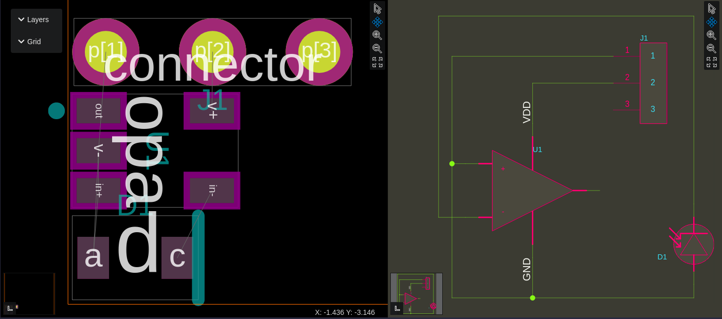
Now that we have land patterns and symbols, CAD can now be exported from this generator.
This section showed you how to create the lowest-level land patterns and symbols and associate them with components. In practice, we spend very little time creating land patterns and symbols like this. Almost everything is generated from a reusable parameterized function, as you will see in the next section.
#use-added-syntax(jitx)
defpackage landpatterns-symbols :
import core
import collections
import math
import jitx
import jitx/commands
import ocdb/utils/symbols
import ocdb/utils/box-symbol
import ocdb/utils/landpatterns
import ocdb/utils/defaults
pcb-pad round-pth-pad :
type = TH
shape = Circle(0.8)
layer(Cutout()) = Circle(0.5)
layer(SolderMask(Top)) = Circle(0.8)
layer(SolderMask(Bottom)) = Circle(0.8)
pcb-landpattern pin-header-landpattern :
pad p[1] : round-pth-pad at loc(-2.54, 0.0)
pad p[2] : round-pth-pad at loc(0.0, 0.0)
pad p[3] : round-pth-pad at loc(2.54, 0.0)
layer(Courtyard(Top)) = Rectangle(6.6, 1.6)
layer(Silkscreen("values", Top)) = Text(">REF", 0.7, C, loc(0.0, -1.2))
pcb-symbol pin-header-symbol :
layer("foreground") = Rectangle(2.54, 7.62, loc(-1.27, 0.0))
for i in 0 to 3 do :
pin p[(i + 1)] at Point(-2.54, (2.54 - (to-double(i) * 2.54))) with :
direction = Left
length = 2.54
number-size = 0.762
name-size = 0.762
preferred-orientation = PreferRotation([0])
layer("reference") = Text(">REF", 0.7056, W, loc(-2.54, 4.2))
pcb-component three-pin-header :
port p : pin[[1 2 3]]
landpattern = pin-header-landpattern(p[1] => pin-header-landpattern.p[1]
p[2] => pin-header-landpattern.p[2]
p[3] => pin-header-landpattern.p[3])
symbol = pin-header-symbol(p[1] => pin-header-symbol.p[1]
p[2] => pin-header-symbol.p[2]
p[3] => pin-header-symbol.p[3])
reference-prefix = "J"
pcb-pad rect-smd-pad :
type = SMD
val pad-shape = Rectangle(0.75, 1.0)
shape = pad-shape
layer(SolderMask(Top)) = pad-shape
layer(Paste(Top)) = pad-shape
pcb-landpattern polarized-chip-landpattern :
pad a : rect-smd-pad at loc(1.0, 0.0)
pad c : rect-smd-pad at loc(-1.0, 0.0)
layer(Courtyard(Top)) = Rectangle(3.0, 2.0)
layer(Silkscreen("pol", Top)) = Line(0.30, [Point((- 1.5), (- 1.0)) Point((- 1.5), 1.0)])
layer(Silkscreen("values", Top)) = Text(">REF", 0.7, C, loc(0.0, -1.2))
pcb-component photodiode :
pin a
pin c
landpattern = polarized-chip-landpattern(a => polarized-chip-landpattern.a,
c => polarized-chip-landpattern.c)
val sym = diode-sym(DiodePhoto)
symbol = sym(a => sym.a,
c => sym.c)
reference-prefix = "D"
pcb-component op-amp :
pin-properties :
[pin:Ref | pads:Int ...]
[in+ | 3 ]
[in- | 4 ]
[out | 1 ]
[v+ | 5 ]
[v- | 2 ]
assign-landpattern(SOT95P280X145-5N)
symbol = op-amp-sym(self.in+ => op-amp-sym.in+
self.in- => op-amp-sym.in-
self.out => op-amp-sym.out
self.v- => op-amp-sym.v-
self.v+ => op-amp-sym.v+)
pcb-module my-design :
inst d : photodiode
inst opa : op-amp
inst connector : three-pin-header
; Set up power connections
net GND (opa.v- connector.p[1])
net VDD (opa.v+ connector.p[2])
; Connect op-amp
net (d.c opa.in-)
net (GND opa.in+ d.a)
make-default-board(my-design, 4, Rectangle(25.0, 25.0))
view-board()
view-schematic()
export-cad()
Parametric CAD
We're going to need some generic parts like resistors and capacitors to finish out our design. In JITX these are generated parametrically, and this section is a deep dive on how that works.
JITX is embedded in a general purpose programming language, so we can write arbitrary software to generate circuitry. Instead of a creating a single design, we write reusable and parametric generators that generate whole families of designs.
Here's how that idea applies to a resistor:
pcb-component example-resistor :
manufacturer = "Yageo"
mpn = "RC0402FR-071KL"
description = "RES SMD 1K OHM 1% 1/16W 0402"
reference-prefix = "R"
port p : pin[[1 2]]
val sym = resistor-sym(ResistorStd)
val lp = ipc-two-pin-landpattern("0402")
symbol = sym(p[1] => sym.p[1], p[2] => sym.p[2])
landpattern = lp(p[1] => lp.p[1], p[2] => lp.p[2])
Some new things here. example-resistor is annotated with a manufacturer, mpn, and a description - information used to build a bill of materials. Let's take a closer look at these four lines:
val sym = resistor-sym(ResistorStd)
val lp = ipc-two-pin-landpattern("0402")
symbol = sym(p[1] => sym.p[1], p[2] => sym.p[2])
landpattern = lp(p[1] => lp.p[1], p[2] => lp.p[2])
Both the symbol and the land pattern are created by parametric functions.
Here's an example generator to explore calling simple parametric generators for symbols and land patterns. Notice that we have imported
land-patternsandsymbolsfrom the library to bring in our previously written functions for generating land patterns and symbols. This generator useschip-resistor, a parametric resistor where we set the properties we care about (resistance, tolerance, power, etc...) and later an automated solver populates a BoM of real devices matching our requirements.
Parametric symbols
resistor-sym is a parametric pcb-symbol that generates different resistor symbols based on the type we request. resistor-sym(ResistorStd) produces a standard resistor symbol, but we could instead call resistor-sym(ResistorPhoto) to generate a photoresistor symbol, as shown below. Check out the implementation (defined in lib/utils/symbols.stanza) to see how the function works (use Go to definition to jump there).
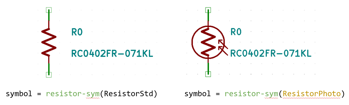
We have written a whole suite of symbol generators, so it's quite rare that you would have to write your own from scratch.
Parametric land patterns
Similarly, ipc-two-pin-landpattern is a function that generates an IPC-compliant nominal material condition land pattern matching the requested land pattern size. Here are the results for 0201 - 0805:
Digging into the implementation of ipc-two-pin-landpattern, (found in lib/utils/land-patterns.stanza -- use Go to definition to jump there) shows how parametrization and reuse can be used to create families of land patterns. This code is heavily factored because each of the functions has standalone utility and gets used elsewhere.
The top-level function we call from our component creates a pcb-landpattern that is parameterized by a string indicating the land pattern size. Inside the land pattern there is a call to another function that will create the geometry based on the size argument.
public pcb-landpattern ipc-two-pin-landpattern (part-name:String) :
make-ipc-two-pin-landpattern(part-name, true)
This function accepts a String as an input, that then matches that string to a set of parameters defining the land pattern geometry, and then pipes those parameters to a function that constructs the geometry. Notice that here we use inside pcb-landpattern : to set the context of this function to give us access to land pattern JITX statements.
public defn make-ipc-two-pin-landpattern (part-name:String, courtyard?:True|False) :
inside pcb-landpattern :
val [Z, G, X, nr, nc] = switch(part-name) :
"0201" : [1.12, 0.20, 0.42, 1.42, 0.92]
"0402" : [1.53, 0.39, 0.62, 1.84, 0.92]
"0603" : [2.55, 0.65, 1.00, 3.10, 1.50]
"0805" : [2.90, 0.90, 2.00, 3.40, 2.00]
"1206" : [4.05, 1.65, 1.80, 4.60, 2.30]
"2512" : [7.35, 4.85, 3.40, 3.90, 7.90]
"1210" : [4.40, 1.20, 2.70, 5.00, 3.00]
"2010" : [6.20, 2.60, 2.70, 7.00, 3.00]
"2920" : [9.70, 5.10, 5.60, 10.0, 6.00]
else : fatal("Unrecognized two pin part name: '%_." % [part-name])
make-two-pin-landpattern(Z, G, X, nr, nc, courtyard?)
ref-label()
This make-two-pin-landpattern function sizes and places pads based on the parameters we give it. Notice the smd-pad(Y,X) statements that construct parametrically sized pads.
public defn make-two-pin-landpattern (Z:Double, G:Double, X:Double, w:Double, h:Double, courtyard?:True|False) :
inside pcb-landpattern :
val Y = (Z - G) / 2.0 ; width of pad
val C2 = (G + Y) / 2.0 ; distance between pad center and land pattern centerline
pad p[1] : smd-pad(Y,X) at loc((- C2), 0.0)
pad p[2] : smd-pad(Y,X) at loc(C2, 0.0)
if courtyard? :
layer(Courtyard(Top)) = Rectangle(w, h)
At the lowest level of hierarchy, we have the smd-pad function that creates a rectangular SMD copper pad with SolderMask and Paste layers. Here we use function overloading so if you call smd-pad with only a X-Y dimension, it sets a default anchor for you.
public defn smd-pad (w:Double, h:Double) :
smd-pad(C,w,h)
public pcb-pad smd-pad (anchor:Anchor, w:Double, h:Double) :
name = to-string("%_x%_ %_ SMD Pad" % [w,h,anchor])
type = SMD
shape = Rectangle(anchor, w, h)
layer(Paste(Top)) = Rectangle(anchor, w, h)
layer(SolderMask(Top)) = Rectangle(anchor, w, h)
It is rare that we have to dig this deep in the library in practice, but we hope the example drilling down to the lowest-level implementation details was illustrative.
Conclusion
To sum up, JITX code and much of OCDB (the JITX standard library) is made out of software functions that generate design information based on parameters. We get high levels of reuse, so we don't have to write much code to generate our designs and once we verify a generator, we know every design it produces will be correct. Also note that OCDB is open-source and yours to change and adapt to your own design preferences.
Furthermore, the native parametrization of JITX gives us a lot of power. Let's say that you would prefer smaller pads for each component to accomodate a dense design, or you want to make sure the soldermask dimensions on pads are adjusted when you are shipping a hi-rel aerospace design. Both are accomplished with a simple extension to the above code, and the change is rolled out globally when we change design parameters, without having to update each component manually.
#use-added-syntax(jitx)
defpackage parametric :
import core
import collections
import math
import jitx
import jitx/commands
import ocdb/utils/defaults
import ocdb/utils/landpatterns
import ocdb/utils/symbols
import ocdb/utils/generic-components
pcb-component example-resistor :
manufacturer = "Yageo"
mpn = "RC0402FR-071KL"
description = "RES SMD 1K OHM 1% 1/16W 0402"
reference-prefix = "R"
port p : pin[[1 2]]
val sym = resistor-sym(ResistorStd)
val lp = ipc-two-pin-landpattern("0402")
symbol = sym(p[1] => sym.p[1], p[2] => sym.p[2])
landpattern = lp(p[1] => lp.p[1], p[2] => lp.p[2])
pcb-module my-design :
inst photo : example-resistor
inst r1 : chip-resistor(["resistance" => 10.0, "case" => "0201"])
inst r2 : chip-resistor(["resistance" => 10.0, "case" => "0402"])
inst r3 : chip-resistor(["resistance" => 10.0, "case" => "0603"])
inst r4 : chip-resistor(["resistance" => 10.0, "case" => "0805"])
for i in instances(self) do :
println(mpn?(i))
make-default-board(my-design, 4, Rectangle(10.0, 10.0))
view-board()
view-schematic()
Modules
We have a good start on our design with models for the starting components of our transimpedance amplifier. Rather than just sticking the components in at the design level, we can define a reusable subcircuit that we can deploy any time we need a transimpedance amplifier.
This section shows you how to create reusable sub-circuits by using the pcb-module statement. Modules in JITX are collections of components, and other modules, connected by nets.
Let's define a reusable module for our transimpedance amplifier. Here is the target circuit
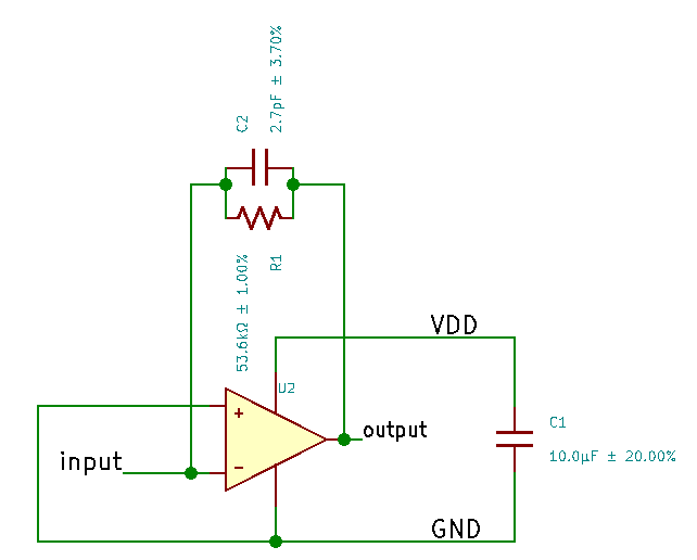
We start our module by transcribing this schematic into a netlist in a pcb-module:
pcb-module transimpedance-amplifier :
pin input
pin output
pin vdd
pin gnd
inst op-amp:op-amp
inst decoupling-cap : ceramic-cap(10.0e-6)
; Connect module pins and decoupling to op-amp power pins.
net (vdd op-amp.v+ decoupling-cap.p[1])
net (gnd op-amp.v- decoupling-cap.p[2])
; Add and connect feedback network
inst r : chip-resistor(closest-std-val(54.0e3, 1.0))
inst c : ceramic-cap(2.7e-12)
net (gnd op-amp.in+)
net (input, op-amp.in-, r.p[1] c.p[1])
net (output op-amp.out, r.p[2] c.p[2])
This module starts with a definition of the ports -- when we use this module in our design, these ports are the only thing we connect to. Pins and ports are used interchangeably in this context.
inputis the input to the amplifieroutputis the output of the amplifiervddis our power pin.gndis our ground pin.
We then instantiate our op-amp and a decoupling capacitor:
inst op-amp:op-amp
inst decoupling-cap : ceramic-cap(10.0e-6)
ceramic-cap is a generic capacitor (similar to chip-resistor that we saw in the last section), here we request a 10.0uF ceramic capacitor.
Often a module will contain a key component and its housekeeping components. (e.g. the
pcb-modulefor the nRF52 contains the bypass capacitors, oscillators, and programming circuitry)
Next, we connect the op-amp to its decoupling capacitor, and importantly to the vdd and gnd pins on our module:
; Connect module pins and decoupling to op-amp power pins.
net (vdd op-amp.v+ decoupling-cap.p[1])
net (gnd op-amp.v- decoupling-cap.p[2])
Forgetting to connect up the gnd and vdd pins would mean that no connection would be made to the actual components, when we later instantiate this module and connect to its ports.
Finally we add the feedback resistor and capacitor, and connect them to our op-amp and the input and ouput pins:
; Add and connect feedback network
inst r : chip-resistor(closest-std-val(54.0e3, 1.0))
inst c : ceramic-cap(2.7e-12)
net (gnd op-amp.in+)
net (input, op-amp.in-, r.p[1] c.p[1])
net (output op-amp.out, r.p[2] c.p[2])
We've picked some static values of ~54.0 kOhm and 2.7pF for our resistor and capacitor closest-std-val is a function from ocdb/utils/generic-components that gives the closest value in the EIA range applying to the tolerance we request. e.g. closest-std-val(54.0e3, 1.0) is the value closest to 54,000.0 in the 1.0% range and turns out to be 53,600.0.
Here is example code for this generator. We can add our transimpedance circuit to our design with a single inst statement:
pcb-module my-design :
inst amp : transimpedance-amplifier
Which results in the correct, but slightly strange looking schematic:
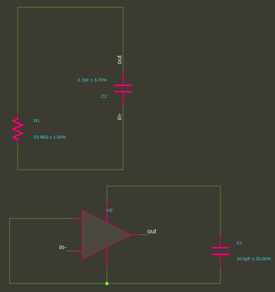
Parameterization
Our module definition isn't too bad, but having the values for the feedback components hardcoded isn't great. Very often we want to make our modules parametric so they become more useful. Let's start by passing in our desired values for the resistor and capacitor:
pcb-module transimpedance-amplifier (rf:Double, cf:Double):
pin input
pin output
pin vdd
pin gnd
inst op-amp:op-amp
inst decoupling-cap : ceramic-cap(10.0e-6)
; Connect module pins and decoupling to op-amp power pins.
net (vdd op-amp.v+ decoupling-cap.p[1])
net (gnd op-amp.v- decoupling-cap.p[2])
; Add and connect feedback network
inst r : chip-resistor(closest-std-val(rf, 1.0))
inst c : ceramic-cap(cf)
net (gnd op-amp.in+)
net (input, op-amp.in-, r.p[1] c.p[1])
net (output op-amp.out, r.p[2] c.p[2])
Now that our module is parametric, let's instantiate two versions of it with different gain resistors that will attach to two photodiodes. We also want a better schematic, so we add net symbols to the power and ground rails and apply logical groupings to the schematic.
pcb-module my-design :
inst d : photodiode[2]
inst high-gain-amp : transimpedance-amplifier(54.0e3, 2.7e-12)
inst low-gain-amp : transimpedance-amplifier(27.0e3, 2.7e-12)
inst connector : pin-header(3)
; Set up power connections
net GND (high-gain-amp.gnd low-gain-amp.gnd connector.p[1])
net VDD (high-gain-amp.vdd low-gain-amp.vdd connector.p[2])
; Connect diodes to amplifiers
net (d[0].c high-gain-amp.input)
net (d[0].a high-gain-amp.gnd)
net (d[1].c low-gain-amp.input)
net (d[1].a low-gain-amp.gnd)
schematic-group(d[0]) = schematic-group(high-gain-amp)
schematic-group(d[1]) = schematic-group(low-gain-amp)
symbol(GND) = ocdb/utils/symbols/ground-sym
symbol(VDD) = ocdb/utils/symbols/supply-sym
Here's a link to the complete tutorial code, which results in the new design:
We now have two diodes connected to transimpedance amplifers that we instantiated using the same parametric module.
When we create parametric modules like this we usually start by transcribing some concrete schematic, and then gradually parameterize it until it captures the design space we care about. And modules can include each other, so this parametric amplifer could be used inside another module that generates and powers the entire analog front end. It's parametric reuse all the way down and all the way up, just like our parametric components.
#use-added-syntax(jitx)
defpackage parametric-modules :
import core
import collections
import math
import jitx
import jitx/commands
import ocdb/utils/symbols
import ocdb/utils/box-symbol
import ocdb/utils/landpatterns
import ocdb/utils/defaults
import ocdb/utils/generic-components
; Our previously-defined components
pcb-pad rect-smd-pad :
type = SMD
val pad-shape = Rectangle(0.75, 1.0)
shape = pad-shape
layer(SolderMask(Top)) = pad-shape
layer(Paste(Top)) = pad-shape
pcb-landpattern polarized-chip-landpattern :
pad a : rect-smd-pad at loc(1.0, 0.0)
pad c : rect-smd-pad at loc(-1.0, 0.0)
layer(Courtyard(Top)) = Rectangle(3.0, 2.0)
layer(Silkscreen("pol", Top)) = Line(0.30, [Point((- 1.5), (- 1.0)) Point((- 1.5), 1.0)])
layer(Silkscreen("values", Top)) = Text(">REF", 0.7, C, loc(0.0, -1.2))
pcb-component photodiode :
pin a
pin c
landpattern = polarized-chip-landpattern(a => polarized-chip-landpattern.a,
c => polarized-chip-landpattern.c)
val sym = diode-sym(DiodePhoto)
symbol = sym(a => sym.a,
c => sym.c)
reference-prefix = "D"
pcb-component op-amp :
pin-properties :
[pin:Ref | pads:Int ...]
[in+ | 3 ]
[in- | 4 ]
[out | 1 ]
[v+ | 5 ]
[v- | 2 ]
assign-landpattern(SOT95P280X145-5N)
symbol = op-amp-sym(self.in+ => op-amp-sym.in+
self.in- => op-amp-sym.in-
self.out => op-amp-sym.out
self.v- => op-amp-sym.v-
self.v+ => op-amp-sym.v+)
; New amplifier circuit
pcb-module transimpedance-amplifier (rf:Double, cf:Double):
pin input
pin output
pin vdd
pin gnd
inst op-amp:op-amp
inst decoupling-cap : ceramic-cap(10.0e-6)
; Connect module pins and decoupling to op-amp power pins.
net (vdd op-amp.v+ decoupling-cap.p[1])
net (gnd op-amp.v- decoupling-cap.p[2])
; Add and connect feedback network
inst r : chip-resistor(closest-std-val(rf, 1.0))
inst c : ceramic-cap(cf)
net (gnd op-amp.in+)
net (input, op-amp.in-, r.p[1] c.p[1])
net (output op-amp.out, r.p[2] c.p[2])
schematic-group(self) = trans-amp
pcb-module my-design :
inst d : photodiode[2]
inst high-gain-amp : transimpedance-amplifier(54.0e3, 2.7e-12)
inst low-gain-amp : transimpedance-amplifier(27.0e3, 2.7e-12)
inst connector : pin-header(3)
; Set up power connections
net GND (high-gain-amp.gnd low-gain-amp.gnd connector.p[1])
net VDD (high-gain-amp.vdd low-gain-amp.vdd connector.p[2])
; Connect diodes to amplifiers
net (d[0].c high-gain-amp.input)
net (d[0].a high-gain-amp.gnd)
net (d[1].c low-gain-amp.input)
net (d[1].a low-gain-amp.gnd)
schematic-group(d[0]) = schematic-group(high-gain-amp)
schematic-group(d[1]) = schematic-group(low-gain-amp)
symbol(GND) = ocdb/utils/symbols/ground-sym
symbol(VDD) = ocdb/utils/symbols/supply-sym
make-default-board(my-design, 4, Rectangle(25.0, 10.0))
view-board()
view-schematic()
Properties and parametric circuits
Thus far we have been using JITX to generate a netlist level design and then export it to CAD. It's a good start towards making our design work reusable, but there is more to electrical design than netlist generation.
For example, we parameterized our transimpedance amplifier by setting the value of the gain resistor -- but what we really care about is that the photodiode and amplifier circuit responds correctly to a change in brightness.
We reach that level of automation by using properties in JITX.
Applying properties
Properties can be applied inside the scope of pcb-components and pcb-modules to pins, components, nets and modules. To apply a property, use a property statement. Here's an example of applying properties inside the definition of our photodiode:
pcb-component photodiode :
pin a
pin c
landpattern = polarized-chip-landpattern(a => polarized-chip-landpattern.a,
c => polarized-chip-landpattern.c)
val sym = diode-sym(DiodePhoto)
symbol = sym(a => sym.a,
c => sym.c)
reference-prefix = "D"
property(self.responsivity) = 125.0e-6 / 1000.0 ; Current out / light in @850nm (A / lux)
Properties support an arbitrary key-value store. So the line property(self.responsivity) = 125.0e-6 / 1000.0 creates a new property entry with the key responsivity and the value 1.25e-7. This is the amount of reverse current (in amps) generated per unit light (in lux).
The key and value can be anything, and we can have as many properties as we like. In a later chapter we'll add the self-capacitance of this photodiode to check the stability of the amplifier.
Using properties
We access properties using the property statement.
property(pd.responsivity) returns the value matching the responsivity key of the pd instance.
pcb-module my-design:
inst pd : photodiode
println("Photodiode responsivity: %_" % [property(pd.responsivity)])
Loading this design in the JITX Shell returns:
stanza> load "props.stanza"
Photodiode responsivity: 1.25e-07
Now that we have this simple property stored, we can use it to automate some design work. Let's write an amplified-photodiode module to calculate appropriate appropriate parameters for the feedback components in the transimpedance amplifier, and create the netlist automatically.
pcb-module amplified-photodiode ( photodiode:Instantiable,
supply-voltage:Double,
lux-at-full-range:Double,
target-bandwidth:Double) :
pin output
pin vdd
pin gnd
inst pd : photodiode
; Calculate 1% gain resistor
val max-light-current = property(pd.responsivity) * lux-at-full-range
val target-gain-resistance = closest-std-val(supply-voltage / max-light-current, 1.0)
; Calculate feedback capacitor for stability at bandwidth
val cf = closest-std-val(1.0 / (2.0 * PI * target-gain-resistance * target-bandwidth) * 0.9, 10.0)
inst amp : transimpedance-amplifier(target-gain-resistance, cf)
net (pd.c amp.input)
net (output amp.output)
net (gnd pd.a amp.gnd)
net (vdd amp.vdd)
schematic-group(pd) = schematic-group(amp)
This module has four arguments, which we have been able to raise to the level of engineering requirements by using properties to drive our parametric transimpedance amplifier from the last section.
photodiodethis is a photodiode from the library that we want to use. It could be any photodiode with theresponsivityproperty defined.supply-voltagewhat voltage do we want to supply to the op-amp?lux-at-full-rangewhat level of light should saturate the output of the amplified photodiode?target-bandwidthup to what bandwidth does the amplifier need to be stable?
After defining the ports, this module creates an instance of the photodiode of the requested type, named pd:
pin output
pin vdd
pin gnd
inst pd : photodiode
Next we calculate the target saturation current based on the light level and the responsivity of the diode, and use that to figure out the target resistance based on the supply voltage. then calculate the target value of the feedback capacitor based on that resistance and the target bandwidth:
; Calculate 1% gain resistor (ti app note TIDU535)
val max-light-current = property(pd.responsivity) * lux-at-full-range
val target-gain-resistance = closest-std-val(supply-voltage / max-light-current, 1.0)
; Calculate feedback capacitor for stability at bandwidth
val cf = closest-std-val(1.0 / (2.0 * PI * target-gain-resistance * target-bandwidth) * 0.9, 10.0)
This simple function assumes rail-to-rail operation on the op-amp, we could make a better version by adding detailed properties to the op-amp, and using them to improve these equations and adjust the circuitry of the amplifier.
Finally we instantiate a transimpedance amplifier using the parameters we calculated, and hook up the photodiode and module ports:
inst amp : transimpedance-amplifier(target-gain-resistance, cf)
net (pd.c amp.input)
net (output amp.output)
net (gnd pd.a amp.gnd)
net (vdd amp.vdd)
In our design we can request two different amplified photodiodes, one that saturates at 500 lux, and one that saturates at 2000 lux (both powered from 3.3V and having at least 1 MHz bandwidth):
pcb-module my-design :
inst high-sensitivity-photodiode : amplified-photodiode(photodiode, 3.3, 500.0, 1.0e6)
inst low-sensitivity-photodiode : amplified-photodiode(photodiode, 3.3, 2000.0, 1.0e6)
inst connector : pin-header(3)
; Set up power connections
net GND (high-sensitivity-photodiode.gnd low-sensitivity-photodiode.gnd connector.p[1])
net VDD (high-sensitivity-photodiode.vdd low-sensitivity-photodiode.vdd connector.p[2])
symbol(GND) = ocdb/utils/symbols/ground-sym
symbol(VDD) = ocdb/utils/symbols/supply-sym
Here's a link to the complete tutorial code, run it to create this new design:
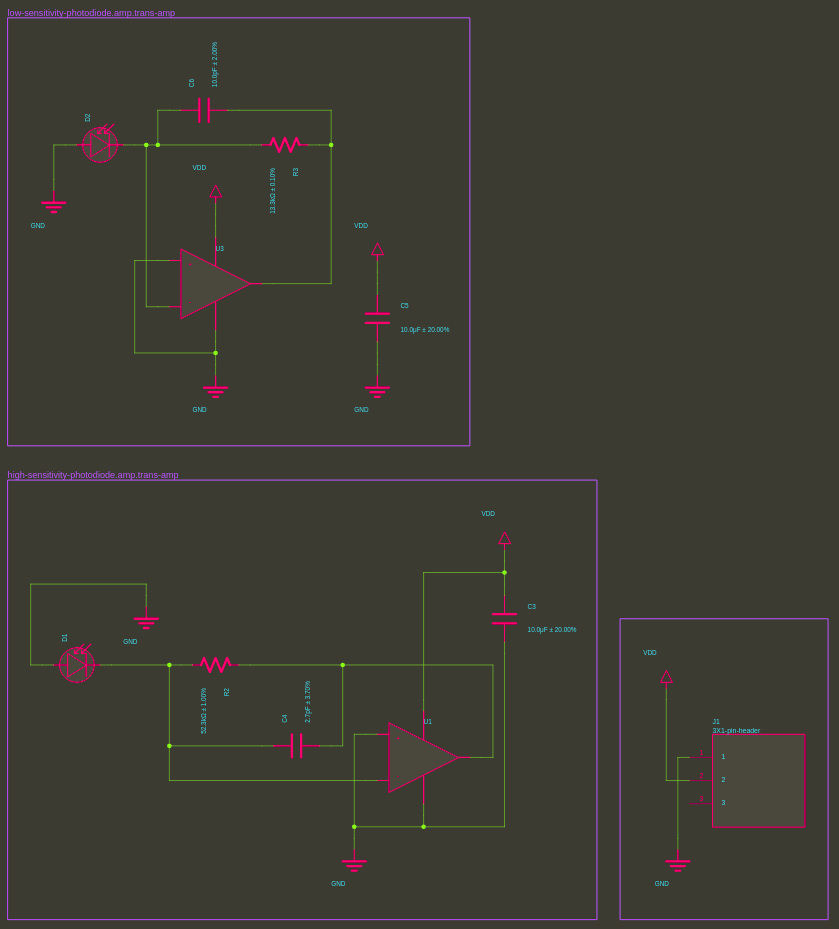
Properties make it possible to go beyond a netlist-level design and parametrically design circuits to automate routine engineering work. The amplified-photodiode function we wrote in this tutorial covers a sizeable design space and could be extended to cover the vast majority of applications.
OCDB makes extensive use of properties to write design generators, especially in the automated design checking functions. We have done some of the leg work to make sure that a useful set of properties are populated for our commonly used components, like the ceramic capacitor:
inst decoupling-cap : ceramic-cap(10.0e-6)
In the low-level design, you can see the detailed component information for the optimal part that was chosen for our design:
inst decoupling-cap (self) :
pcb-component D12968 :
name = "my-capacitor"
manufacturer = "Samsung Electro-Mechanics"
mpn = "CL05A106MP8NUB8"
pin-array p:pin[1, 2] :
pin p[1]
pin p[2]
symbol = D12757 :
package = D12761 :
spice :
"[C] (p[1]) (p[2]) 1.0e-05"
emodel = Capacitor(1.0e-05, 20.0, 10.0, false, UNKNOWN, "X5R")
reference-prefix = "C"
property(self.capacitor) = true
property(self.trust) = "low"
property(self.x) = 1.0
property(self.y) = 0.5
property(self.z) = 0.9
property(self.mounting) = "smd"
property(self.rated-temperature) = [-55.0 85.0]
property(self.case) = "0402"
property(self.metadata) = ["datasheets" => "//media.digikey.com/pdf/Data%20Sheets/Samsung%20PDFs/CL05A106MP8NUB8_Spec.pdf" "image" => "//media.digikey.com/Renders/Samsung%20Electro-Mechanics%20America/0805-(1.40)-CL-Series.jpg" "digi-key-part-number" => "1276-6830-6-ND" "unit-price" => "Digi-Reel" "packaging" => "Digi-Reel®" "series" => "CL" "applications" => "General Purpose"]
property(self.type) = "ceramic"
property(self.tolerance) = [-0.2 0.2]
property(self.capacitance) = 1.0e-05
property(self.anode) = false
property(self.electrolyte) = false
property(self.temperature-coefficient) = "X5R"
property(self.rated-voltage) = 10.0
property(self.rated-current-pk) = false
property(self.rated-current-rms) = false
So while we design we'll be able to draw on a database of several million components, focusing on building automation and not data entry.
#use-added-syntax(jitx)
defpackage props :
import core
import collections
import math
import jitx
import jitx/commands
import ocdb/utils/symbols
import ocdb/utils/box-symbol
import ocdb/utils/landpatterns
import ocdb/utils/defaults
import ocdb/utils/generic-components
; Our previously-defined components
pcb-pad rect-smd-pad :
type = SMD
val pad-shape = Rectangle(0.75, 1.0)
shape = pad-shape
layer(SolderMask(Top)) = pad-shape
layer(Paste(Top)) = pad-shape
pcb-landpattern polarized-chip-landpattern :
pad a : rect-smd-pad at loc(1.0, 0.0)
pad c : rect-smd-pad at loc(-1.0, 0.0)
layer(Courtyard(Top)) = Rectangle(3.0, 2.0)
layer(Silkscreen("pol", Top)) = Line(0.30, [Point((- 1.5), (- 1.0)) Point((- 1.5), 1.0)])
layer(Silkscreen("values", Top)) = Text(">REF", 0.7, C, loc(0.0, -1.2))
pcb-component photodiode :
pin a
pin c
landpattern = polarized-chip-landpattern(a => polarized-chip-landpattern.a,
c => polarized-chip-landpattern.c)
val sym = diode-sym(DiodePhoto)
symbol = sym(a => sym.a,
c => sym.c)
reference-prefix = "D"
property(self.responsivity) = 125.0e-6 / 1000.0 ; Current out / light in @850nm (A / lux)
pcb-component op-amp :
pin-properties :
[pin:Ref | pads:Int ...]
[in+ | 3 ]
[in- | 4 ]
[out | 1 ]
[v+ | 5 ]
[v- | 2 ]
assign-landpattern(SOT95P280X145-5N)
symbol = op-amp-sym(self.in+ => op-amp-sym.in+
self.in- => op-amp-sym.in-
self.out => op-amp-sym.out
self.v- => op-amp-sym.v-
self.v+ => op-amp-sym.v+)
pcb-module transimpedance-amplifier (rf:Double, cf:Double):
pin input
pin output
pin vdd
pin gnd
inst op-amp:op-amp
inst decoupling-cap : ceramic-cap(10.0e-6)
; Connect module pins and decoupling to op-amp power pins.
net (vdd op-amp.v+ decoupling-cap.p[1])
net (gnd op-amp.v- decoupling-cap.p[2])
; Add and connect feedback network
inst r : chip-resistor(closest-std-val(rf, 1.0))
inst c : ceramic-cap(cf)
net (gnd op-amp.in+)
net (input, op-amp.in-, r.p[1] c.p[1])
net (output op-amp.out, r.p[2] c.p[2])
schematic-group(self) = trans-amp
; New function
pcb-module amplified-photodiode ( photodiode:Instantiable,
supply-voltage:Double,
lux-at-full-range:Double,
target-bandwidth:Double) :
pin output
pin vdd
pin gnd
inst pd : photodiode
; Calculate 1% gain resistor TIDU535
val max-light-current = property(pd.responsivity) * lux-at-full-range
val target-gain-resistance = closest-std-val(supply-voltage / max-light-current, 1.0)
; Calculate feedback capacitor for stability at bandwidth
val cf = closest-std-val(1.0 / (2.0 * PI * target-gain-resistance * target-bandwidth) * 0.9, 10.0)
inst amp : transimpedance-amplifier(target-gain-resistance, cf)
net (pd.c amp.input)
net (output amp.output)
net (gnd pd.a amp.gnd)
net (vdd amp.vdd)
schematic-group(pd) = schematic-group(amp)
pcb-module my-design :
inst high-sensitivity-photodiode : amplified-photodiode(photodiode, 3.3, 500.0, 1.0e6)
inst low-sensitivity-photodiode : amplified-photodiode(photodiode, 3.3, 2000.0, 1.0e6)
inst connector : pin-header(3)
; Set up power connections
net GND (high-sensitivity-photodiode.gnd low-sensitivity-photodiode.gnd connector.p[1])
net VDD (high-sensitivity-photodiode.vdd low-sensitivity-photodiode.vdd connector.p[2])
symbol(GND) = ocdb/utils/symbols/ground-sym
symbol(VDD) = ocdb/utils/symbols/supply-sym
make-default-board(my-design, 4, Rectangle(25.0, 10.0))
view-board()
view-schematic()
Bundles
A pcb-bundle is a collection of pins. Usually we create bundles to group pins that we want to keep together. For example we can create a bundle for an i2c bus with the following statement:
pcb-bundle i2c:
pin sda
pin scl
When to Use Bundles
Bundles are useful when you have any system which has multiple connections that you want to connect at once, such as:
- connectors
- busses
- GPIO
- protocols (SPI, I2C, etc.)
Tutorial
Now that our photodiodes are in order, we want to quickly bring up the rest of our design, which will be connected with interfaces like i2c and spi. We manage those connections in JITX using bundles.
We can use our new bundle to define i2c interfaces on components and wire them up. For example, let's say we want to connect a thermocouple amplifier to a microcontroller using an i2c bus.
pcb-component thermocouple-amplifier :
manufacturer = "Microchip"
mpn = "MCP9600"
description = "Thermocouple EMF to Temperature Converter, ±1.5°C Maximum Accuracy"
port i2c-node : i2c
pin-properties :
[pin:Ref | pads:Int ... | side:Dir ]
[GND | 1, 3, 5, 6, 7, 9, 10, 13, 17, 18, 21 | Down ]
[Vin+ | 2 | Right ]
[Vin- | 4 | Right ]
[Vdd | 8 | Up ]
[Alert[1] | 11 | Left ]
[Alert[2] | 12 | Left ]
[Alert[3] | 14 | Left ]
[Alert[4] | 15 | Left ]
[ADDR | 16 | Left ]
[i2c-node.scl | 19 | Left ]
[i2c-node.sda | 20 | Left ]
make-box-symbol()
assign-landpattern(qfn-landpattern(0.65, 5.0, 20, 0.3, 0.4, [3.25 3.25]))
pcb-component microcontroller :
port i2c-controller : i2c
pin-properties :
[pin:Ref | pads:Int ... | side:Dir]
[i2c-controller.scl | 1 | Right]
[i2c-controller.sda | 2 | Right]
for i in 3 to 14 do :
[PA[i] | i + 1 | Right]
[vdd | 15 | Up]
[gnd | 16 | Down]
make-box-symbol()
assign-landpattern(soic127p-landpattern(16))
pcb-module my-design :
inst K : thermocouple-amplifier
inst mcu : microcontroller
net (K.i2c-node, mcu.i2c-controller)
inst high-sensitivity-photodiode : amplified-photodiode(photodiode, 3.3, 500.0, 1.0e6)
net (high-sensitivity-photodiode.output mcu.PA[4])
In our thermocouple-amplifier component, port i2c-node : i2c defines a port named i2c-node and sets the type to be i2c. i2c-node now has the two pins from the i2c bundle, sda and scl. We can then assign the pins of the i2c-node port to concrete land pattern pads.
We then add a similar port to the MCU named i2c-controller and assign it to concrete pads on the land pattern.
After we instantiate these components in our design, we can directly connect the i2c ports together using the net statement. JITX does the work to go into the bundle and connect scl to scl and sda to sda, so at the end of the day pin 19 on the light sensor gets connected to pin 1 on the micro controller.
This direct connection works with bundles of identical type, no matter how complex. It's an easy way to reduce errors in our design - when we connect i2c ports there is no way to accidentally connect sda to scl.
Here's a link to the complete tutorial code you can run to produce this design. Here is a portion of the schematic showing our i2c connection:
Complex bundles
pcb-bundles can include other bundles hierarchically, with as many layers of hierarchy as we need. Let's create a bundle for a DDR3 interface.
pcb-bundle diff-pair:
pin P
pin N
pcb-bundle ddr3-data :
port ck : diff-pair
port ldqs : diff-pair
port udqs : diff-pair
port ba : pin[3]
port a : pin[15]
port dq : pin[16]
pin cke
pin odt
pin nCS
pin nRAS
pin nCAS
pin nWE
pin dmu
pin dml
pin nRESET
pcb-bundle ddr3-power :
pin vddq
pin vssq
pin vdd
pin vss
pin vrefdq
pin vrefca
pin zq
pcb-bundle ddr3 :
port data : ddr3-data
port power : ddr3-power
We first define a bundle for a differential pair, with pins N and P. We then use that bundle inside a new ddr3-data bundle for the DDR3 clock, and data strobes. The ddr3 data bundle also includes banks of address and data pins and the control pins. We then create a ddr3-power bundle with the supply and reference voltages. Finally we wrap ddr3-data and ddr3-power up into a single ddr3 bundle.
We can still access the low-level pins using the . operator: ddr3.data.ck.P gets us the positive pin of the DDR3 clock. (ddr3.data.clk would get us the differential pair). More importantly, we don't have to fuss with the low-level pins because we can net the top level bundles together:
net (FPGA.ddr3, SDRAM.ddr3)
This net statement connects a total of 56 pins from an FPGA to your SDRAM, making sure everything is connected correctly by recursively connecting all of the sub-bundles.
(You can create parametric bundles if you wanted to capture the full scope of all possible DDR3 connections (x4 x8, etc...).)
#use-added-syntax(jitx)
defpackage props :
import core
import collections
import math
import jitx
import jitx/commands
import ocdb/utils/symbols
import ocdb/utils/box-symbol
import ocdb/utils/landpatterns
import ocdb/utils/defaults
import ocdb/utils/generic-components
; Our previously-defined components
pcb-pad rect-smd-pad :
type = SMD
val pad-shape = Rectangle(0.75, 1.0)
shape = pad-shape
layer(SolderMask(Top)) = pad-shape
layer(Paste(Top)) = pad-shape
pcb-landpattern polarized-chip-landpattern :
pad a : rect-smd-pad at loc(1.0, 0.0)
pad c : rect-smd-pad at loc(-1.0, 0.0)
layer(Courtyard(Top)) = Rectangle(3.0, 2.0)
layer(Silkscreen("pol", Top)) = Line(0.30, [Point((- 1.5), (- 1.0)) Point((- 1.5), 1.0)])
layer(Silkscreen("values", Top)) = Text(">REF", 0.7, C, loc(0.0, -1.2))
pcb-component photodiode :
pin a
pin c
landpattern = polarized-chip-landpattern(a => polarized-chip-landpattern.a,
c => polarized-chip-landpattern.c)
val sym = diode-sym(DiodePhoto)
symbol = sym(a => sym.a,
c => sym.c)
reference-prefix = "D"
property(self.responsivity) = 125.0e-6 / 1000.0 ; Current out / light in @850nm (A / lux)
pcb-component op-amp :
pin-properties :
[pin:Ref | pads:Int ...]
[in+ | 3 ]
[in- | 4 ]
[out | 1 ]
[v+ | 5 ]
[v- | 2 ]
assign-landpattern(SOT95P280X145-5N)
symbol = op-amp-sym(self.in+ => op-amp-sym.in+
self.in- => op-amp-sym.in-
self.out => op-amp-sym.out
self.v- => op-amp-sym.v-
self.v+ => op-amp-sym.v+)
pcb-module transimpedance-amplifier (rf:Double, cf:Double):
pin input
pin output
pin vdd
pin gnd
inst op-amp:op-amp
inst decoupling-cap : ceramic-cap(10.0e-6)
; Connect module pins and decoupling to op-amp power pins.
net (vdd op-amp.v+ decoupling-cap.p[1])
net (gnd op-amp.v- decoupling-cap.p[2])
; Add and connect feedback network
inst r : chip-resistor(closest-std-val(rf, 1.0))
inst c : ceramic-cap(cf)
net (gnd op-amp.in+)
net (input, op-amp.in-, r.p[1] c.p[1])
net (output op-amp.out, r.p[2] c.p[2])
schematic-group(self) = trans-amp
pcb-module amplified-photodiode ( photodiode:Instantiable,
supply-voltage:Double,
lux-at-full-range:Double,
target-bandwidth:Double) :
pin output
pin vdd
pin gnd
inst pd : photodiode
; Calculate 1% gain resistor TIDU535
val max-light-current = property(pd.responsivity) * lux-at-full-range
val target-gain-resistance = closest-std-val(supply-voltage / max-light-current, 1.0)
; Calculate feedback capacitor for stability at bandwidth
val cf = closest-std-val(1.0 / (2.0 * PI * target-gain-resistance * target-bandwidth) * 0.9, 10.0)
inst amp : transimpedance-amplifier(target-gain-resistance, cf)
net (pd.c amp.input)
net (output amp.output)
net (gnd pd.a amp.gnd)
net (vdd amp.vdd)
schematic-group(pd) = schematic-group(amp)
; New code
pcb-bundle i2c:
pin sda
pin scl
pcb-component thermocouple-amplifier :
manufacturer = "Microchip"
mpn = "MCP9600"
description = "Thermocouple EMF to Temperature Converter, ±1.5°C Maximum Accuracy"
port i2c-node : i2c
pin-properties :
[pin:Ref | pads:Int ... | side:Dir ]
[GND | 1, 3, 5, 6, 7, 9, 10, 13, 17, 18, 21 | Down ]
[Vin+ | 2 | Right ]
[Vin- | 4 | Right ]
[Vdd | 8 | Up ]
[Alert[1] | 11 | Left ]
[Alert[2] | 12 | Left ]
[Alert[3] | 14 | Left ]
[Alert[4] | 15 | Left ]
[ADDR | 16 | Left ]
[i2c-node.scl | 19 | Left ]
[i2c-node.sda | 20 | Left ]
make-box-symbol()
assign-landpattern(qfn-landpattern(0.65, 5.0, 20, 0.3, 0.4, [3.25 3.25]))
pcb-component microcontroller :
port i2c-controller : i2c
pin-properties :
[pin:Ref | pads:Int ... | side:Dir]
[i2c-controller.scl | 1 | Right]
[i2c-controller.sda | 2 | Right]
for i in 3 to 14 do :
[PA[i] | i + 1 | Right]
[vdd | 15 | Up]
[gnd | 16 | Down]
make-box-symbol()
assign-landpattern(soic127p-landpattern(16))
pcb-module my-design :
inst K : thermocouple-amplifier
inst mcu : microcontroller
net (K.i2c-node, mcu.i2c-controller)
inst high-sensitivity-photodiode : amplified-photodiode(photodiode, 3.3, 500.0, 1.0e6)
net (high-sensitivity-photodiode.output mcu.PA[4])
inst connector : pin-header(3)
; Set up power connections
net GND (high-sensitivity-photodiode.gnd connector.p[1] mcu.gnd K.GND)
net VDD (high-sensitivity-photodiode.vdd connector.p[2] mcu.vdd K.Vdd)
symbol(GND) = ocdb/utils/symbols/ground-sym
symbol(VDD) = ocdb/utils/symbols/supply-sym
make-default-board(my-design, 4, Rectangle(25.0, 10.0))
view-board()
view-schematic()
Pin assignment
Just like we improved our amplifier design by removing the need to hard-code details (like the gain resistor resistance), we can write more reusable code by solving for pin assignments rather than hard-coding them. This allows us to easily swap complex components like microcontrollers and FPGAs in our designs.
Very often there are multiple ways to correctly connect the components on a board. i.e. we don't care that this 3rd and 4th pins on our sensor are connected to the 1st and 2nd pins on our microcontroller, but rather that the i2c interface on the sensor is connected to pins on the microcontroller that support i2c. In this section we solve this problem using the support and require statements, and finish our design.
Microcontroller example
Let's start with a small microcontroller we want to connect to our photodiodes, sensor, and a LORA modem. We want to model for a 16-pin microcontroller with a SOIC land pattern that supports a variety of interfaces:
- 14 GPIO
- 3 ADCs
- 2 SPI
- 1 I2C
This particular device has the ability to map any GPIO and SPI pin to any device pin (i.e. it has a fully populated matrix IO for these interfaces). Here is the model:
pcb-component microcontroller :
pin-properties :
[pin:Ref | pads:Int ... | side:Dir]
for i in 0 to 14 do :
[PA[i] | i + 1 | Right]
[vdd | 15 | Up]
[gnd | 16 | Down]
make-box-symbol()
assign-landpattern(soic127p-landpattern(16))
supports adc:
adc.adc => self.PA[0]
supports adc:
adc.adc => self.PA[1]
supports adc:
adc.adc => self.PA[2]
supports i2c :
i2c.sda => self.PA[10]
i2c.scl => self.PA[11]
pcb-bundle io-pin :
pin p
for i in 0 to 14 do :
supports io-pin :
io-pin.p => self.PA[i]
for i in 0 to 2 do :
supports spi-controller():
require io:io-pin[4]
spi-controller().copi => io[0].p
spi-controller().cipo => io[1].p
spi-controller().cs => io[2].p
spi-controller().sck => io[3].p
for i in 0 to 14 do:
supports gpio:
require io:io-pin
gpio.gpio => io.p
The support statement here indicates that the component supports a pcb-bundle on a particular set of pins. We have imported ocdb/utils/bundles to pull in the standard bundles.
In this case we are using these bundles to model the peripherals present on the MCU IC. Translating the above model:
- The MCU has ADC capable inputs on pins
PA[0],PA[1], andPA[2] - There is one
i2cport available on pinsPA[10]andPA[11]
We then define a dummy interface io-pin to represent the pins that can perform any GPIO or SPI function. In the support statement, we require as many of these pins as we need (e.g. 4 for a standard spi-controller), and then map them to the bundle pins. Here:
- There are two available SPI ports
- There are 14 available GPIO pins
Example generator
Here is a link to an example generator for experimenting with pin assignment.
We can connect to supported bundles using the require statement and the pin assignment solver in JITX will either come up with a valid concrete pin assignment, or indicate that no solution is possible. Let's break down the require statements in the main module.
The following statement requests a bundle called light of type adc[2] from our instance of the microcontroller, mcu.
require light:adc[2] from mcu
Now light exists as a bundle of type adc[2] (i.e. two adc pins named light[0] and light[1]) associated with the mcu. Later, the pin solver will find two concrete pins on the mcu that supports adc, and replace light[0] and light[1] in the netlist with a reference to those pins. Because light is guaranteed to exist, we can use it like a real bundle and net the adc pins in the bundle to the outputs of our transimpedance amplifiers:
net (high-sensitivity-photodiode.output light[0].adc)
net (low-sensitivity-photodiode.output light[1].adc)
Similarly, we can require an i2c bundle, 4 gpio, and an spi-controller bundle from the MCU and connect them to the components on the board. Note that OCDB distinguishes between SPI controllers and peripherals and we used connect-spi (imported from ocdb/utils/connects) to make the connection instead of a net statement (because the bundles are different).
And here is our final design:
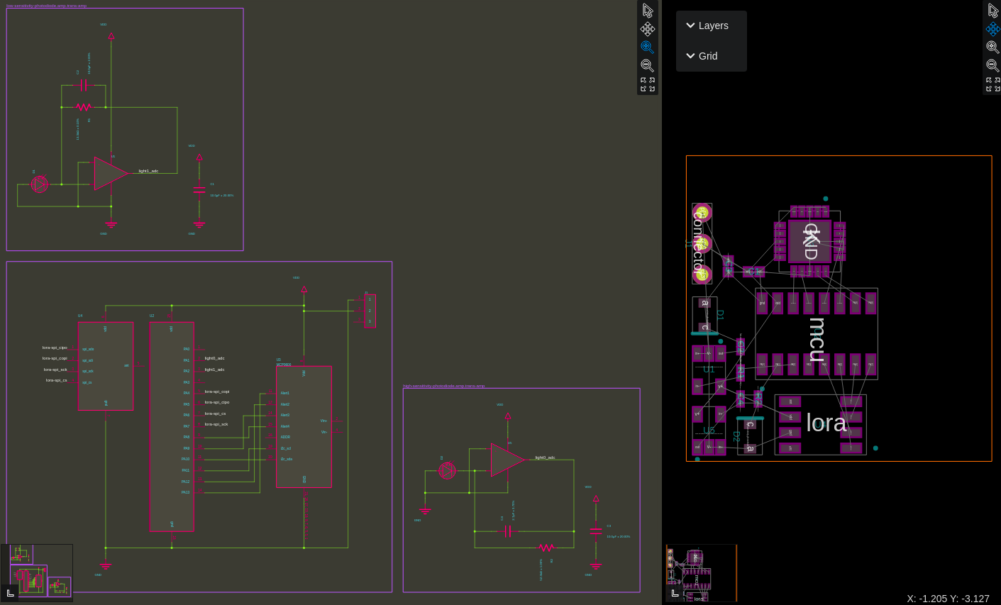
The solver is clever, and ensures that it doesn't reserve a pin for gpio that is required by and i2c or adc pin. You can play with this generator to test the capabilities of the solver for yourself. Furthermore supports and require works at the module level as well, so you can have a bundle supported by a collection of circuitry, not just by a component.
So now we have worked through from the fundamentals of JITX to a design built from reusable code. You should be able to do most things in JITX now - reach out if you have any questions!
#use-added-syntax(jitx)
defpackage first-design :
import core
import math
import jitx
import jitx/commands
import ocdb/utils/defaults
import ocdb/utils/landpatterns
import ocdb/utils/symbols
import ocdb/utils/symbol-utils
import ocdb/utils/generic-components
import ocdb/utils/bundles
import ocdb/utils/box-symbol
import ocdb/utils/property-structs
import ocdb/utils/connects
pcb-component lora-modem :
port spi : spi-peripheral()
pin-properties :
[pin:Ref | pads:Int ... | side:Dir]
[spi.sdo | 1 | Left]
[spi.sdi | 2 | Left]
[spi.sck | 3 | Left]
[spi.cs | 4 | Left]
[ant | 5 | Right]
[vdd | 6 | Up]
[gnd | 7 | Down]
make-box-symbol()
assign-landpattern(soic127p-landpattern(8))
pcb-component microcontroller :
pin-properties :
[pin:Ref | pads:Int ... | side:Dir]
for i in 0 to 14 do :
[PA[i] | i + 1 | Right]
[vdd | 15 | Up]
[gnd | 16 | Down]
make-box-symbol()
assign-landpattern(soic127p-landpattern(16))
supports adc:
adc.adc => self.PA[0]
supports adc:
adc.adc => self.PA[1]
supports adc:
adc.adc => self.PA[2]
supports i2c :
i2c.sda => self.PA[10]
i2c.scl => self.PA[11]
pcb-bundle io-pin :
pin p
for i in 0 to 14 do :
supports io-pin :
io-pin.p => self.PA[i]
for i in 0 to 2 do :
supports spi-controller():
require io:io-pin[4]
spi-controller().copi => io[0].p
spi-controller().cipo => io[1].p
spi-controller().cs => io[2].p
spi-controller().sck => io[3].p
for i in 0 to 14 do:
supports gpio:
require io:io-pin
gpio.gpio => io.p
pcb-component thermocouple-amplifier :
manufacturer = "Microchip"
mpn = "MCP9600"
description = "Thermocouple EMF to Temperature Converter, ±1.5°C Maximum Accuracy"
port i2c : i2c
pin-properties :
[pin:Ref | pads:Int ... | side:Dir ]
[GND | 1, 3, 5, 6, 7, 9, 10, 13, 17, 18, 21 | Down ]
[Vin+ | 2 | Right ]
[Vin- | 4 | Right ]
[Vdd | 8 | Up ]
[Alert[1] | 11 | Left ]
[Alert[2] | 12 | Left ]
[Alert[3] | 14 | Left ]
[Alert[4] | 15 | Left ]
[ADDR | 16 | Left ]
[i2c.scl | 19 | Left ]
[i2c.sda | 20 | Left ]
make-box-symbol()
assign-landpattern(qfn-landpattern(0.65, 5.0, 20, 0.3, 0.4, [3.25 3.25]))
pcb-component op-amp :
pin-properties :
[pin:Ref | pads:Int ...]
[in+ | 3 ]
[in- | 4 ]
[out | 1 ]
[v+ | 5 ]
[v- | 2 ]
assign-landpattern(SOT95P280X145-5N)
symbol = op-amp-sym(self.in+ => op-amp-sym.in+
self.in- => op-amp-sym.in-
self.out => op-amp-sym.out
self.v- => op-amp-sym.v-
self.v+ => op-amp-sym.v+)
pcb-pad round-pth-pad :
type = TH
shape = Circle(0.8)
layer(SolderMask(Top)) = Circle(0.8)
layer(SolderMask(Bottom)) = Circle(0.8)
layer(Cutout()) = Circle(0.5)
pcb-symbol pin-header-symbol :
layer("foreground") = Rectangle(2.54, 7.62, loc(-1.27, 0.0))
for i in 0 to 3 do :
pin p[(i + 1)] at Point(-2.54, (2.54 - (to-double(i) * 2.54))) with :
direction = Left
length = 2.54
number-size = 0.762
name-size = 0.762
preferred-orientation = PreferRotation([0])
layer("reference") = Text(">REF", 0.7056, W, loc(-2.54, 4.2))
pcb-landpattern pin-header-landpattern :
pad p[1] : round-pth-pad at loc(-2.54, 0.0)
pad p[2] : round-pth-pad at loc(0.0, 0.0)
pad p[3] : round-pth-pad at loc(2.54, 0.0)
layer(Courtyard(Top)) = Rectangle(6.6, 1.6)
layer(Silkscreen("values", Top)) = Text(">REF", 0.7, C, loc(0.0, -1.2))
pcb-component three-pin-header :
port p : pin[[1 2 3]]
landpattern = pin-header-landpattern(p[1] => pin-header-landpattern.p[1]
p[2] => pin-header-landpattern.p[2]
p[3] => pin-header-landpattern.p[3])
symbol = pin-header-symbol(p[1] => pin-header-symbol.p[1]
p[2] => pin-header-symbol.p[2]
p[3] => pin-header-symbol.p[3])
reference-prefix = "J"
pcb-pad rect-smd-pad :
type = SMD
val pad-shape = Rectangle(0.75, 1.0)
shape = pad-shape
layer(SolderMask(Top)) = pad-shape
layer(Paste(Top)) = pad-shape
pcb-landpattern polarized-chip-landpattern :
pad a : rect-smd-pad at loc(1.0, 0.0)
pad c : rect-smd-pad at loc(-1.0, 0.0)
layer(Courtyard(Top)) = Rectangle(3.0, 2.0)
layer(Silkscreen("pol", Top)) = Line(0.30, [Point((- 1.5), (- 1.0)) Point((- 1.5), 1.0)])
layer(Silkscreen("values", Top)) = Text(">REF", 0.7, C, loc(0.0, -1.2))
pcb-component photodiode :
pin a
pin c
landpattern = polarized-chip-landpattern(a => polarized-chip-landpattern.a,
c => polarized-chip-landpattern.c)
val sym = diode-sym(DiodePhoto)
symbol = sym(a => sym.a,
c => sym.c)
reference-prefix = "D"
property(self.responsivity) = 125.0e-6 / 1000.0 ; Current out / light in @850nm (A / lux)
property(self.capacitance) = 11.0e-12 ; Self capacitance (F)
pcb-module transimpedance-amplifier (rf:Double, cf:Double):
pin input
pin output
pin vdd
pin gnd
inst op-amp:op-amp
inst decoupling-cap : ceramic-cap(10.0e-6)
; Connect module pins and decoupling to op-amp power pins.
net (vdd op-amp.v+ decoupling-cap.p[1])
net (gnd op-amp.v- decoupling-cap.p[2])
; Add and connect feedback network
inst r : chip-resistor(closest-std-val(rf, 1.0))
inst c : ceramic-cap(cf)
net (gnd op-amp.in+)
net (input, op-amp.in-, r.p[1] c.p[1])
net (output op-amp.out, r.p[2] c.p[2])
schematic-group(self) = trans-amp
pcb-module amplified-photodiode ( photodiode:Instantiable,
supply-voltage:Double,
lux-at-full-range:Double,
target-bandwidth:Double) :
pin output
pin vdd
pin gnd
inst pd : photodiode
; Calculate 1% gain resistor TIDU535
val max-light-current = property(pd.responsivity) * lux-at-full-range
val target-gain-resistance = closest-std-val(supply-voltage / max-light-current, 1.0)
; Calculate feedback capacitor for stability at bandwidth
val cf = closest-std-val(1.0 / (2.0 * PI * target-gain-resistance * target-bandwidth) * 0.9, 10.0)
inst amp : transimpedance-amplifier(target-gain-resistance, cf)
net (pd.c amp.input)
net (output amp.output)
net (gnd pd.a amp.gnd)
net (vdd amp.vdd)
schematic-group(pd) = schematic-group(amp)
pcb-module main-design :
inst connector : three-pin-header
inst mcu : microcontroller
net GND (connector.p[1] mcu.gnd)
net VDD (connector.p[2] mcu.vdd)
inst high-sensitivity-photodiode : amplified-photodiode(photodiode, 3.3, 500.0, 1.0e6)
inst low-sensitivity-photodiode : amplified-photodiode(photodiode, 3.3, 2000.0, 1.0e6)
require light:adc[2] from mcu
net (high-sensitivity-photodiode.output light[0].adc)
net (low-sensitivity-photodiode.output light[1].adc)
inst K : thermocouple-amplifier
require K-i2c : i2c from mcu
require alert:gpio[4] from mcu
net (K-i2c, K.i2c)
for i in 0 to 4 do :
net (alert[i].gpio, K.Alert[i + 1])
inst lora : lora-modem
require lora-spi:spi-controller() from mcu
connect-spi(mcu, lora-spi, [lora.spi])
net (GND high-sensitivity-photodiode.gnd low-sensitivity-photodiode.gnd K.GND lora.gnd)
net (VDD high-sensitivity-photodiode.vdd low-sensitivity-photodiode.vdd K.Vdd lora.vdd)
symbol(GND) = ocdb/utils/symbols/ground-sym
symbol(VDD) = ocdb/utils/symbols/supply-sym
set-current-design("first-design")
make-default-board(main-design, 4, Rectangle(25.0, 25.0))
; Export CAD with default options
export-cad()
; Show the Schematic and PCB for the design
view-board()
view-schematic()
Model a power regulator
This tutorial walks you through creating a simple parametric regulator using the AP2205 adjustable LDO from Diodes Incorporated, and adding it as a component library. We'll walk through creating a new project, adding a new component to an existing library, modelling the main IC, and then follow up with a parametric module to solve for any desired output voltage.
Contents
- Model a power regulator
Setting up the code
Create a new project
First, create a new project
Create a new component
Next, click on the JITX pane and select "Create component." Make a new folder named components and choose it as the parent directory. Name the component file AP2205. This will create a file called <your-component-name>.stanza, but you should type in only the component name (not the .stanza file extension).
Add the components library to stanza.proj
Copy-paste this line into the stanza.proj file to import all the component files in /components/ into our project.
packages components/* defined-in "components" ; notice the extra s
Modeling the Component
Update the Pin Properties
Initially our component definition looks like this :
public pcb-component component :
name = "AP2205"
description = "PART, DESCRIPTION, DETAILED"
mpn = "MANUFACTURER PART NUMBER"
manufacturer = "MANUFACTURER NAME"
reference-prefix = "LETTER"
pin-properties :
[pin:Ref | pads:Int ... | side:Dir ]
[VCC | 1 | Up ]
[GND | 6 | Down ]
[PINNAME1 | 2 | Left ]
[PINNAME2 | 3 | Right ]
[PINNAME3 | 4 | Left ]
[PINNAME4 | 5 | Right ]
make-box-symbol()
assign-landpattern(lp-AP2205)
supports power:
power.vdd => self.VCC
power.gnd => self.GND
We need to update this with the information from the datasheet.
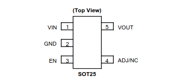
public pcb-component component :
name = "AP2205"
description = "Adjustable LDO Regulator"
mpn = "AP2205-W5-7"
manufacturer = "Diodes Incorporated"
reference-prefix = "U"
pin-properties :
[pin:Ref | pads:Int ... | side:Dir ]
[vin | 1 | Left ]
[gnd | 2 | Down ]
[enable | 3 | Left ]
[adj | 4 | Down ]
[vout | 5 | Right ]
make-box-symbol()
assign-landpattern(lp-AP2205)
Reload the design to view the changes. You'll notice that the schematic symbol is updated.
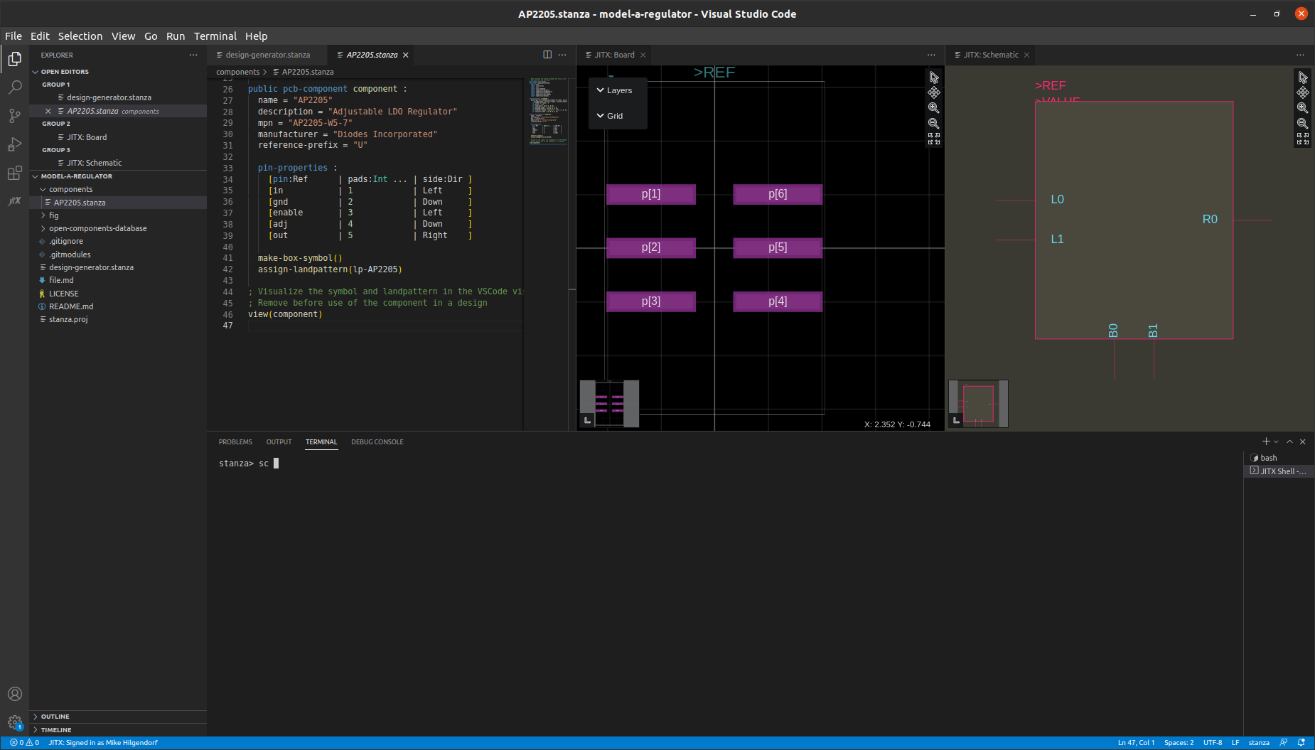
We've also removed the supports power statement - we won't need it in this example.
Finally we add some electrical properties that enable automatic design and checking.
public pcb-component component :
name = "AP2205"
description = "Adjustable LDO Regulator"
mpn = "AP2205-W5-7"
manufacturer = "Diodes Incorporated"
reference-prefix = "U"
pin-properties :
[pin:Ref | pads:Int ... | side:Dir ]
[vin | 1 | Left ]
[gnd | 2 | Down ]
[enable | 3 | Left ]
[adj | 4 | Down ]
[vout | 5 | Right ]
make-box-symbol()
assign-landpattern(lp-AP2205)
val gen-props = ocdb/utils/property-structs/GenericPin(min-max(0.0, 36.0), 1000.0)
property(self.vin.generic-pin) = gen-props
property(self.enable.generic-pin) = gen-props
property(self.vin.generic-pin) = gen-props
property(self.vin.power-pin) = ocdb/utils/property-structs/PowerPin(min-max(2.3, 24.0))
property(self.adj.vref) = 1.24
property(self.vout.max-current) = 250.0e-3
Model the Landpattern
We need to model the SOT-25 landpattern required by this part. By default the component creation tool makes an SOIC landpattern with the call to make-n-pin-soic-landpattern. We'll replace this with another generator from ocdb/utils/landpatterns called make-dual-row-smd-landpattern which creates two rows of pads with different pitches and numbers of pins.
Don't copy paste this. This code block is already built in to JITX.
public defn make-dual-row-smd-landpattern (
primary-num-pins: Int, ; number of pins on one side of the land pattern
secondary-num-pins: Int, ; number of pins on the other side of the land pattern
primary-pin-pitch: Double, ; the pitch of pins on the primary side of the land pattern
secondary-pin-pitch: Double, ; the pitch of the pins on the other side of the land pattern
lead-span: Toleranced, ; the lead span across the land pattern
package-length: Toleranced, ; the length of the package
package-width: Toleranced, ; the width of the package
terminal-length: Toleranced, ; the length of the terminals
terminal-width: Toleranced) : ; the width of the terminals
To do this we remove the body of lp-AP2205 first :
pcb-landpattern lp-AP2205 :
And add a call to make-dual-row-smd-landpattern
pcb-landpattern lp-AP2205 :
make-dual-row-smd-landpattern(
primary-num-pins, secondary-num-pins,
primary-pin-pitch, secondary-pin-pitch,
lead-span, package-length, package-width,
terminal-length, terminal-width)
We don't have values for each of these fields yet, so let's add a where : clause and fill them in.
pcb-landpattern lp-AP2205 :
make-dual-row-smd-landpattern(
primary-num-pins, secondary-num-pins,
primary-pin-pitch, secondary-pin-pitch,
lead-span, package-length, package-width,
terminal-length, terminal-width) where :
val primary-num-pins =
val secondary-num-pins =
val primary-pin-pitch =
val secondary-pin-pitch =
val lead-span =
val package-length =
val package-width =
val terminal-length =
val terminal-width =
We grab the actual values from the data sheet :
pcb-landpattern lp-AP2205 :
make-dual-row-smd-landpattern(
primary-num-pins, secondary-num-pins,
primary-pin-pitch, secondary-pin-pitch,
lead-span, package-length, package-width,
terminal-length, terminal-width) where :
val primary-num-pins = 3
val secondary-num-pins = 2
val primary-pin-pitch = 0.95 ; D
val secondary-pin-pitch = 2.0 * primary-pin-pitch
val lead-span = min-typ-max(2.70, 2.80, 3.00) ; C
val package-length = min-typ-max(2.90, 3.00, 3.10) ; H
val package-width = min-typ-max(1.50, 1.60, 1.70) ; B
val terminal-length = min-typ-max(0.35, 0.40, 0.55) ; L
val terminal-width = min-typ-max(0.35, 0.38, 0.50) ; A
Reloading the component will show the component with its correct landpattern.
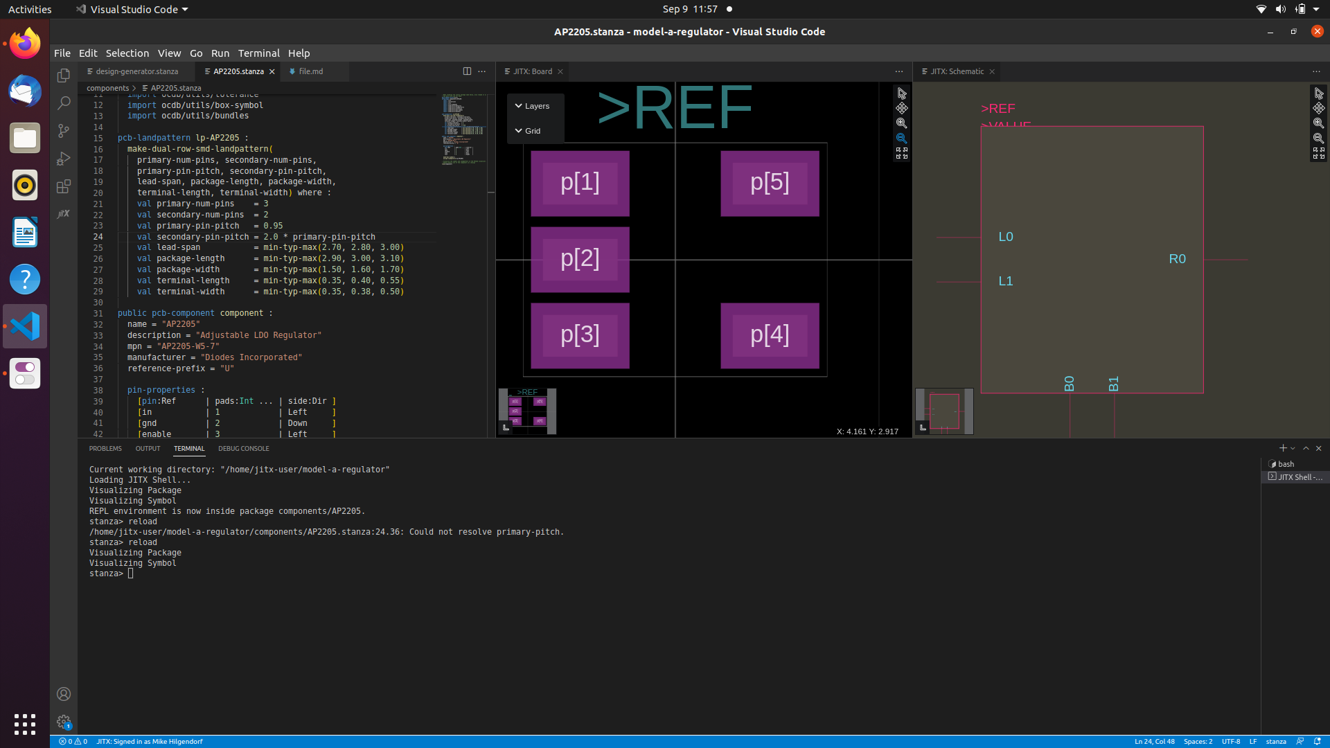
Create a Solver
The adjustable LDO is only useful if we can place it in a circuit. Instead of forcing users of the library to compute their resistor values each time they use the LDO, we can write a module generator that will solve for the resistor values for a desired output voltage.
Define the pcb-module
First we'll define a new module that takes vout as an argument.
public pcb-module module (vout:Double) :
Now let's define the input/output ports. We will have two ports for voltage, in and out that can be net to other power ports in the design, and an enable pin for the LDO.
; inside pcb-module
port in : power
port out : power
pin enable
Now we can add the LDO and wire power and ground nets. We also add input and output capacitors to the ldo.
; Instantiate the component
inst ldo : components/AP2205/component
; Wire up the LDO to the module ports
net VIN (ldo.vin, in.vdd)
net VOUT (ldo.vout, out.vdd)
net GND (ldo.gnd, in.gnd, out.gnd)
net (ldo.enable, enable)
cap-strap(ldo.vin, ldo.gnd, 1.0e-6)
cap-strap(ldo.vout, ldo.gnd, 2.2e-6)
In order to make our call to cap-strap work, we need to import the generic components. Paste the below line with the other import statements.
import ocdb/utils/generic-components
Finally we use the voltage-divider solver to design the feedback network for us and then we connect it up.
inst output-voltage-divider : ocdb/modules/passive-circuits/voltage-divider(source-voltage = high-voltage, divider-output = adj-voltage, tolerance = tolerance, current = current) where :
val high-voltage = vout
val adj-voltage = property(ldo.adj.vref) as Double
val tolerance = 1.0
val current = 0.5e-3
net (output-voltage-divider.in, ldo.vout)
net (output-voltage-divider.out, ldo.adj)
net (output-voltage-divider.lo, ldo.gnd)
Add to the main.stanza design generator
In your project's main.stanza you can now instantiate the component module
pcb-module my-design :
inst version-label : ocdb/artwork/board-text/version-silkscreen("Version 0.0")
place(version-label) at loc(0.0, height(board-shape) / 2.0 - 1.0) on Bottom
inst p3v3 : components/AP2205/module(3.3)
inst p1v5 : components/AP2205/module(1.5)
net GND (p3v3.in.gnd p1v5.in.gnd)
symbol(GND) = ocdb/utils/symbols/ground-sym
schematic-group(p3v3) = Power_3v3
schematic-group(p1v5) = Power_1v5
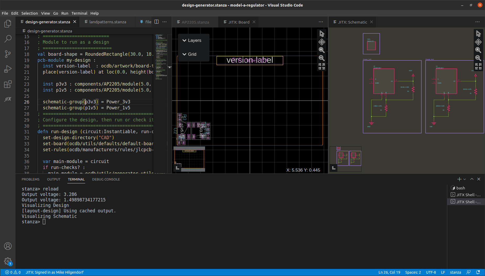
Adding Electrical Properties for checks
JITX includes advanced mechanisms for checking the electrical properties of a design, but these checks typically involve adding some property values to components and nets.
First we need to update the defpackage statement to include some helper structs from ocdb :
#use-added-syntax(jitx)
defpackage components/AP2205:
import core
import collections
import jitx
import jitx/commands
import ocdb/utils/defaults
import ocdb/utils/landpatterns
import ocdb/utils/box-symbol
import ocdb/utils/bundles
import ocdb/utils/generic-components
import ocdb/utils/property-structs ; <--- helpers for checks
See the code for the complete design
We'll be using the following :
GenericPin: Generic pin properties (absolute maximum ratings for voltage and ESD)PowerPin: Properties for power pins (recommended input voltage range)PowerSupplyPin: Properties for pins that supply power (voltage range, maximum current)
We can get the values we need from the absolute maximum ratings table in the datasheet, compute the values we need, and add to the pin-properties table.
public pcb-component component :
name = "AP2205"
description = "Adjustable LDO Regulator"
mpn = "AP2205-W5-7"
manufacturer = "Diodes Incorporated"
reference-prefix = "U"
; Compute the power and generic pin properties
val recommended-voltage = min-max(2.3, 24.0)
val maximum-voltage = typ(36.0)
val esd-voltage = 1000.0
val power-props = PowerPin(recommended-voltage)
val gen-props = GenericPin(maximum-voltage, esd-voltage)
val max-output-current = 250.0e-3
pin-properties :
[pin:Ref | pads:Int ... | side:Dir | generic-pin:GenericPin | power-pin:PowerPin | max-current:Double ]
[in | 1 | Left | gen-props | power-props | - ]
[gnd | 2 | Down | gen-props | - | - ]
[enable | 3 | Left | gen-props | - | - ]
[adj | 4 | Down | gen-props | - | - ]
[out | 5 | Right | gen-props | - | max-output-current ]
Note: since we are using an adjustable LDO, we don't know what the output voltage of the component is, and can't assign a
PowerSupplyPinto its pin properties yet!
Now we need to update the module to assign the power supply pin property to the LDO, and a net voltage property on the output, at the very end of the module.
; Assign the property to the LDO's output pin. We lookup the
; maximum current using the `property(...)` introspection.
property(ldo.out.power-supply-pin) =
PowerSupplyPin(output-voltage, property(ldo.out.max-current))
Final Notes
There is more detail we could add to this model to catch the details like maximum pin voltage and current, which are not captured by a simple netlist. Later tutorials will show you how to capture details that will validate this circuit automatically, so we will have confidence that our design will work.
; When renaming the stanza package name below, also rename it in the folder stanza.proj
; See docs.jitx.com for help
#use-added-syntax(jitx)
defpackage components/AP2205:
import core
import collections
import jitx
import jitx/commands
import ocdb/utils/defaults
import ocdb/utils/landpatterns
import ocdb/utils/box-symbol
import ocdb/utils/bundles
import ocdb/utils/generic-components
import ocdb/utils/property-structs ; <--- helpers for checks
pcb-landpattern lp-AP2205 :
make-dual-row-smd-landpattern(
primary-num-pins, secondary-num-pins,
primary-pin-pitch, secondary-pin-pitch,
lead-span, package-length, package-width,
terminal-length, terminal-width) where :
val primary-num-pins = 3
val secondary-num-pins = 2
val primary-pin-pitch = 0.95
val secondary-pin-pitch = 2.0 * primary-pin-pitch
val lead-span = min-typ-max(2.70, 2.80, 3.00)
val package-length = min-typ-max(2.90, 3.00, 3.10)
val package-width = min-typ-max(1.50, 1.60, 1.70)
val terminal-length = min-typ-max(0.35, 0.40, 0.55)
val terminal-width = min-typ-max(0.35, 0.38, 0.50)
public pcb-component component :
name = "AP2205"
description = "Adjustable LDO Regulator"
mpn = "AP2205-W5-7"
manufacturer = "Diodes Incorporated"
reference-prefix = "U"
; Compute the power and generic pin properties
val recommended-voltage = min-max(2.3, 24.0)
val maximum-voltage = typ(36.0)
val esd-voltage = 1000.0
val power-props = PowerPin(recommended-voltage)
val gen-props = GenericPin(maximum-voltage, esd-voltage)
val max-output-current = 250.0e-3
pin-properties :
[pin:Ref | pads:Int ... | side:Dir ]
[vin | 1 | Left ]
[gnd | 2 | Down ]
[enable | 3 | Left ]
[adj | 4 | Down ]
[vout | 5 | Right ]
make-box-symbol()
assign-landpattern(lp-AP2205)
property(self.vin.generic-pin) = gen-props
property(self.enable.generic-pin) = gen-props
property(self.vin.generic-pin) = gen-props
property(self.vin.power-pin) = ocdb/utils/property-structs/PowerPin(recommended-voltage)
property(self.adj.vref) = min-typ-max(1.215, 1.24, 1.265)
property(self.vout.max-current) = 250.0e-3
public pcb-module module (vout:Double) :
port in : power
port out : power
pin enable
; Instantiate the component
inst ldo : components/AP2205/component
; Wire up the LDO to the module ports
net VIN (ldo.vin, in.vdd)
net VOUT (ldo.vout, out.vdd)
net GND (ldo.gnd, in.gnd, out.gnd)
net (ldo.enable, enable)
cap-strap(ldo.vin, ldo.gnd, 1.0e-6)
cap-strap(ldo.vout, ldo.gnd, 2.2e-6)
inst output-voltage-divider : ocdb/modules/passive-circuits/voltage-divider(source-voltage = high-voltage, divider-output = adj-voltage, tolerance = tolerance, current = current) where :
val high-voltage = vout
val adj-voltage = typ(property(ldo.adj.vref))
val tolerance = 1.0
val current = 0.5e-3
net (output-voltage-divider.in, ldo.vout)
net (output-voltage-divider.out, ldo.adj)
net (output-voltage-divider.lo, ldo.gnd)
symbol(GND) = ocdb/utils/symbols/ground-sym
; Assign the property to the LDO's output pin. We lookup the
; maximum current using the `property(...)` introspection.
property(ldo.vout.power-supply-pin) =
ocdb/utils/property-structs/PowerSupplyPin(typ(vout), property(ldo.vout.max-current) as Double)
Write a check
In this tutorial we will write a check that checks the automotive qualification of a passive component. We will over:
- Writing a check
- Adding a check to a
pcb-module - Running checks
- Inspecting a design to add checks programatically.
The design
Example code for this tutorial is here.
Let's start with a simple design that contains one resistor, with that has a property aec-rating set to "Q200".
pcb-module checked-design :
inst r : chip-resistor(1.0)
property(r.aec-rating) = "Q200"
set-current-design("test-checks")
make-default-board(checked-design, 4, Rectangle(25.0, 25.0))
; Show the Schematic and PCB for the design
view-board()
view-schematic()
The pcb-check
Next we want to define a new check that makes sure that a property named aec-rating exists, and its value is "Q200".
pcb-check aec-q200 (component:JITXObject):
#CHECK(
name = "Automotive rating"
description = "Check that a passive component is AEC Q200 rated"
condition = has-property?(component.aec-rating),
category = "Component Data"
subcheck-description = "Check that %_ has a defined aec-rating" % [ref(component)],
pass-message = "%_ has a property for aec-rating of %_" % [ref(component) property(component.aec-rating)],
info-message = "%_ does not have an aec-rating property attached" % [ref(component)],
locators = [instance-definition(component)]
)
#CHECK(
name = "Automotive rating"
description = "Check that a passive component is AEC Q200 rated"
condition = property(component.aec-rating) == "Q200",
category = "Component Checks"
subcheck-description = "Check that %_ is AEC Q200 rated." % [ref(component)],
pass-message = "%_ is AEC Q200 rated" % [ref(component)],
fail-message = "%_ is not AEC Q200 rated. Instead has rating %_." % [ref(component) property(component.aec-rating)],
locators = [instance-definition(component)]
)
This check takes a JITXObject as an argument. We pass in a component and the #CHECK macros:
- first make sure that the
aec-ratingproperty exists on the component (adding a prompt to add it if it is missing) - and second make sure that the value of
aec-ratingis"Q200".
The syntax of the #CHECK macro is documented here.
In our design, we can check the instance r for an AEC rating with check aec-q200(r):
pcb-module checked-design :
inst r : chip-resistor(1.0)
property(r.aec-rating) = "Q200"
check aec-q200(r)
set-current-design("test-checks")
make-default-board(checked-design, 4, Rectangle(25.0, 25.0))
; Show the Schematic and PCB for the design
view-board()
view-schematic()
run-checks("check-report.txt")
Note that we also add run-checks to run the check we added to our design.
Adding checks with introspection
Let's say that we want to check the AEC rating of any resistor or capacitor in our design. We can write a function that inspects all the components to see if it is a resistor or capacitor, and than applies the check if so. Here's the introspection function and how it gets used in a design with more components:
defn check-aec (module:JITXObject) :
inside pcb-module:
for c in component-instances(self) do :
if has-property?(c.resistance) or reference-prefix?(c) == "R" or
has-property?(c.capacitance) or reference-prefix?(c) == "C" :
check aec-q200(c)
pcb-module checked-design :
inst r : chip-resistor(1.0)[10]
inst c : ceramic-cap(10.0e-6)[8]
for i in [0 1 3 4 5 7] do :
property(r[i].aec-rating) = "Q200"
property(c[i].aec-rating) = "Q200"
property(r[2].aec-rating) = "Q101"
; check aec-q200(r[0])
check-aec(self)
The finished code for the Write a check tutorial
#use-added-syntax(jitx)
defpackage check-report :
import core
import math
import jitx
import jitx/commands
import ocdb/utils/defaults
import ocdb/utils/generic-components
pcb-check aec-q200 (component:JITXObject):
#CHECK(
name = "Automotive rating"
description = "Check that a passive component is AEC Q200 rated"
condition = has-property?(component.aec-rating),
category = "Component Data"
subcheck-description = "Check that %_ has a defined aec-rating" % [ref(component)],
pass-message = "%_ has a property for aec-rating of %_" % [ref(component) property(component.aec-rating)],
info-message = "%_ does not have an aec-rating property attached" % [ref(component)],
locators = [instance-definition(component)]
)
#CHECK(
name = "Automotive rating"
description = "Check that a passive component is AEC Q200 rated"
condition = property(component.aec-rating) == "Q200",
category = "Component Checks"
subcheck-description = "Check that %_ is AEC Q200 rated." % [ref(component)],
pass-message = "%_ is AEC Q200 rated" % [ref(component)],
fail-message = "%_ is not AEC Q200 rated. Instead has rating %_." % [ref(component) property(component.aec-rating)],
locators = [instance-definition(component)]
)
defn check-aec (module:JITXObject) :
inside pcb-module:
for c in component-instances(self) do :
if has-property?(c.resistance) or reference-prefix?(c) == "R" or
has-property?(c.capacitance) or reference-prefix?(c) == "C" :
check aec-q200(c)
pcb-module checked-design :
inst r : chip-resistor(1.0)[10]
inst c : ceramic-cap(10.0e-6)[8]
for i in [0 1 3 4 5 7] do :
property(r[i].aec-rating) = "Q200"
property(c[i].aec-rating) = "Q200"
property(r[2].aec-rating) = "Q101"
check aec-q200(r[0])
check-aec(self)
set-current-design("test-checks")
make-default-board(checked-design, 4, Rectangle(25.0, 25.0))
; Show the Schematic and PCB for the design
view-board()
view-schematic()
run-checks("check-report.txt")
Analyze a Design
This tutorial shows how to create data for electrical checks by analyzing a design. Our goal here is to automate a large amount of analysis, even if our design does not contain enough information to run something like a SPICE simulation on every component.
It will cover:
- Assigning
voltage - Running passes on a
pcb-module - Calculating operating points.
voltage
We enable analysis of our design by assign a voltage property to nets in our design whose voltage we know. e.g.
net P3V3 (mcu.vdd, ldo.vout)
property(P3V3.voltage) = tol%(3.3, 2.0)
voltage is a Toleranced value that represents the range of voltage we expect on this net during normal operation. Defining voltage for nets like power rails enables many checks to run automatically.
Here's a small design setting the voltage on the two pins of a resistor and trying to run checks to check that the operating point of the resistor does not exceed its derated limits.
#use-added-syntax(jitx)
defpackage analysis :
import core
import jitx
import jitx/commands
import ocdb/utils/generic-components
import ocdb/utils/checks
pcb-module design :
inst r : chip-resistor(100.0)
net vdd (r.p[1])
net gnd (r.p[2])
property(vdd.voltage) = tol%(3.3, 5.0)
property(gnd.voltage) = typ(0.0)
ocdb/utils/checks/check-design(self)
set-main-module(design)
run-checks("checks.txt")
When we run this design, we get a failed check prompting us to add information:
r is missing properties: operating-point
Even through we set a voltage on the each net that attaches to the resistor pins:
- The pins of the resistor do not automatically inherit the
voltagefrom the nets they are attached to - The voltage and current across the resistor are not automatically calculated, so the
operating-pointis missing.
We use a pass named run-final-passes to perform these analysis operations.
Running passes on a pcb-module
We can use passes to do many things, including performing analysis on our designs. A pass takes an Instantiable like a pcb-module definition, and returns a transformed version (see transform-module). OCDB has a standard analysis pass named run-final-passes. We use it to transform our design module into an analyzed module with voltages propagated from nets to pins, and operating-point calculated when the necessary information exists.
We call the run-final-passes like this:
val analyzed-design = ocdb/utils/generator-utils/run-final-passes(design) ; Analyze design with a pass
Note that we now need to use analyzed-design as the main-module, so our checks will run on the new transformed version and not the pre-analyzed version. All together the design looks like this:
#use-added-syntax(jitx)
defpackage analysis :
import core
import jitx
import jitx/commands
import ocdb/utils/generic-components
pcb-module design :
inst r : chip-resistor(100.0)
net vdd (r.p[1])
net gnd (r.p[2])
property(gnd.voltage) = typ(0.0)
property(vdd.voltage) = tol%(3.3, 5.0)
ocdb/utils/checks/check-design(self)
val analyzed-design = ocdb/utils/generator-utils/run-final-passes(design)
set-main-module(analyzed-design)
run-checks("checks.txt")
Now when we see missing operating-point show up, it often means we need to add a voltage property to another net in our design.
Revise Existing CAD Designs In JITX
We can revise Kicad or Altium designs in JITX.
Revising an Existing KiCad Design in JITX
In this tutorial, we will walk through modifying an existing KiCAD design in JITX by adding sourcing information to resistors and capacitors, adding an LED circuit, and editing a land pattern. Then, we'll export the design from JITX to KiCAD, and update the layout.
You'll need:
- KiCad
- A KiCad project
This tutorial uses the KiCAD files for the open source Goldfish design.
Contents:
- Import the KiCad Project to JITX
- Make changes to the project
- Export the JITX Project to KiCad
- Update the layout
- Rapid changes we can make in JITX
- Summary
Import the KiCad Project to JITX
Follow the workflow outlined in Importing KiCad to JITX to bring your project into JITX.
For this project, we used:
#use-added-syntax(jitx)
defpackage my-design :
import core
import jitx/commands
import-kicad("Goldfish/cad", "imported-Goldfish", [`overwrite => false])
Make changes to the project
Let's make the following changes:
- Set Project Parameters
- Change the Capacitors to find in-stock Components
- Change the Resistors to find in-stock Components
- Add a power LED
- Edit a land pattern
Let's open the generated file by pressing Ctrl+p and typing goldfish.stanza or double clicking on goldfish.stanza in the explorer window. Then go to File then Save As... and save it as promicro.stanza, because it is a variant of a Pro Micro Arduino.
We'll make edits to this new file. Having the original file will be useful in case we want to do a file compare on our changes later.
We'll visualize the imported design by opening the output folder in VSCode and running from the VSCode terminal:
jitx repl promicro.stanza
We can then rearrange our windows to see the generated code, the schematic, and the layout.
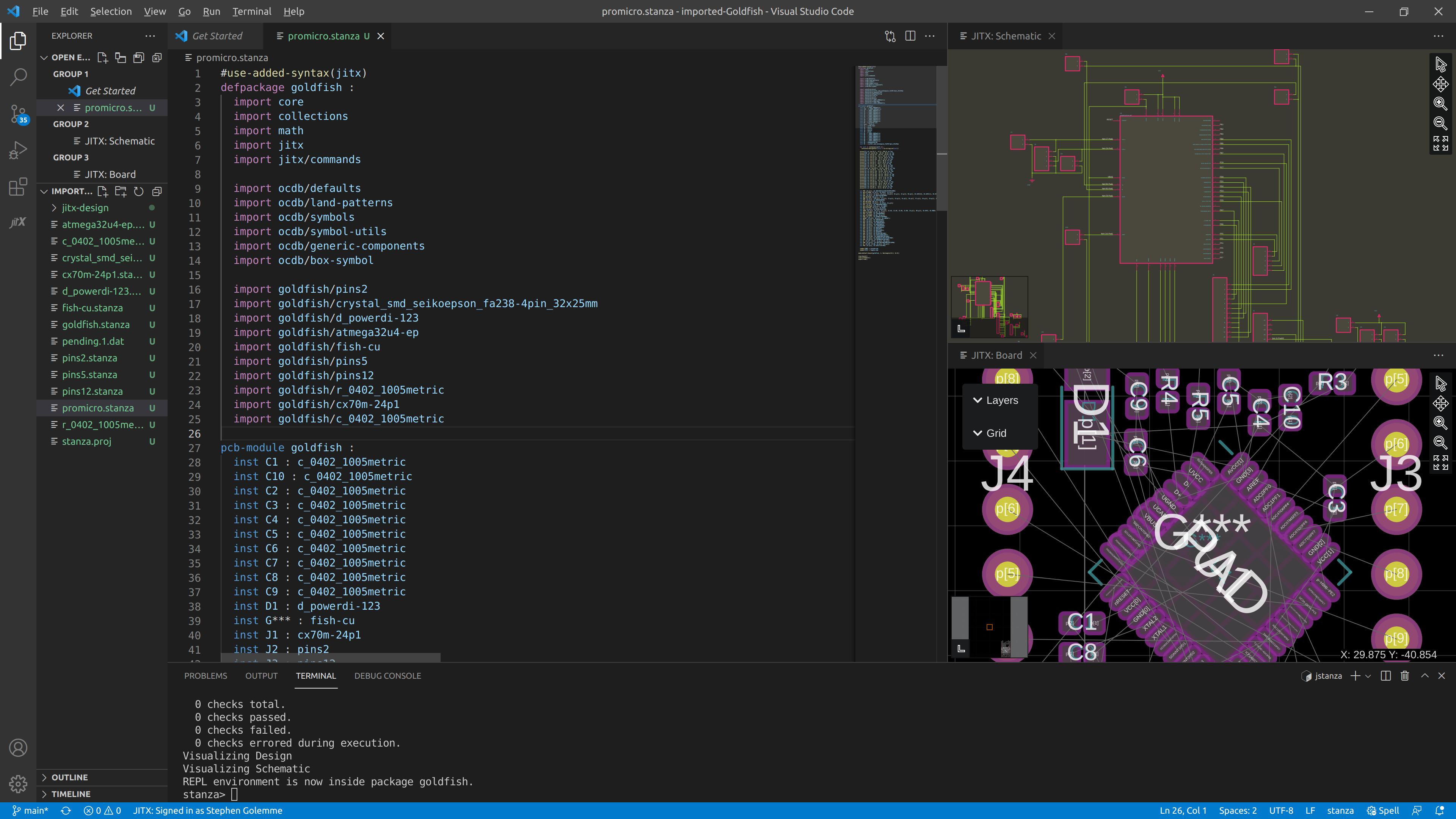
Tip: As we make changes, we can periodically test our code by saving
promicro.stanza, then typingreloadat the stanza prompt.
The last set of imports shows the components imported from KiCAD. A quick glance tells us that all of the resistors and capacitors are brought in as generic r_0402_1005metric or c_0402_1005metric.
Let's start replacing them with JITX functions for capacitors and resistors that return manufacturer part numbers. We'll have to look at the KiCad schematic for the values that were manually added to each part.
The KiCad schematic:
Change the Capacitors to find in-stock Components
We can update each capacitor instance to use the ceramic-cap( function.
inst C9 : c_0402_1005metric
becomes
inst C9 : ceramic-cap(1.0e-6)
Since the maximum voltage on this board is 5 Volts (with the exception of Vin), We'll specify a project level minimum capacitor voltage of 10.0 volts, specifying a 100% headroom. We also specify a project level operating temperature. You can easily change inputs on a project level scale. If we're comfortable with less headroom, we can specify 6.3 Volts.
Right after the imports section of this file, We'll specify some project level parameters for package size, design quantity, and capacitor voltage. (note indentation):
import ocdb/utils/design-vars
OPERATING-TEMPERATURE = min-max(0.0 40.0)
OPTIMIZE-FOR = ["area"]
MIN-PKG = "0402"
DESIGN-QUANTITY = 100
MIN-CAP-VOLTAGE = 10.0
This will select the cheapest capacitor that meets our specifications, 0402, with a minimum distributor stock to make 100 of this design, whenever a sourcing tool is called.
We can go through the rest of the design and replace capacitors in this manner. If we want to specify a higher minimum voltage for a specific capacitor, we can add "min-rated-voltage" => 25.0 to the capacitor function.
Change the Resistors to find in-stock Components
Let's update each resistor instance to use the chip-resistor( function.
inst R1 : r_0402_1005metric
becomes
inst R1 : chip-resistor(5.1e3)
Let's save and type reload followed by Enter in the command line to see the results.
Replace the Schottky diode with one from OCDB
The diode D1 is a generic SOD-123 Schottky diode. We can search file contents for OCDB by pressing Ctrl+Shift+F and searching for schottky. Double-click on a result that's located in open-components-database/ that has SOD123 near the word Schottky. We can copy the MPN and see if it's in stock at our favorite distributor. And we can replace the D1 call with this component by copying the text after defpackage, then calling the component name.
inst D1 : d_powerdi-123
becomes
inst D1 : ocdb/components/on-semiconductor/MBR0520L/component
Let's save and type reload followed by Enter in the command line. to see the results. The command line returns [Error] Cannot access named field 'p'.
A search of promicro.stanza for D1 with a space before it shows 3 results: where D1 is instantiated, net VCC, and net VBUS. The pins are attached to the net with D1.p[1] and looking at the component we selected, we see the available pins are a and c. We'll change D1.p[1] to D1.c and D1.p[2] to D1.a, press Ctrl+S and then type reload and Enter. Now our design loads. It's also a bit easier to read that VCC is the cathode of the diode.
Add a power LED
Next, we'll place a power LED circuit. Let's search for an in-stock 5mA 0603 LED on a distributor website and create a part. I found the Inolux IN-S63BT5UW to have a high mcd rating, 0603 package, 5mA, and a Vf of 3V.
We'll open one of the imported component files, d_powerdo-123.stanza, to quickly glance at what we need to create a component. Copy the contents of this file and press Ctrl+N to create a new file. Then paste the contents into this new file.
The second line defined the package name. Replace d_powerdi-123 with our new package name, IN-S63BT5UW. So the line reads:
defpackage goldfish/IN-S63BT5UW :
Then, press Ctrl+S to save the file. We'll save the file as IN-S63BT5UW.stanza.
Next, after public pcb-component change d_powerdi-123 to component so the line reads:
public pcb-component component :
Press Ctrl+S to save again.
To add an instance of this to promicro.stanza, we'll need to add links in 3 places. First, we need to tell the JITX Shell where to look to find this. Open stanza.proj in the imported-goldfish directory and add a line in the same format as the others:
package goldfish/IN-S63BT5UW defined-in "IN-S63BT5UW.stanza"
Don't forget to save! In promicro.stanza, add a new import statement at the end in the same format as the others:
import goldfish/IN-S63BT5UW`
Finally, after pcb-module goldfish :, add an instance of the part and place it at location 0.0, 0.0 with rotation 0.0 so we can easily find it and watch changes:
pcb-module goldfish :
inst LED1 : goldfish/IN-S63BT5UW/component
place(LED1) at loc(0.0, 0.0, 0.0) on Top
Note: We defined the LED model in a package named
goldfish/IN-S63BT5UWand in that package named the definitioncomponent. The full path of the component is<package>/<definition>and in this example:goldfish/IN-S63BT5UW/component
Save and type reload at the stanza prompt. If it reloads with no errors, we know we've tied everything together correctly.
Add a Land Pattern
Let's use the IPC land pattern generator for this part. First, open the datasheet to see what part dimensions are specified (we do not use the recommended land pattern):
- length = 1.60
- width = 0.80
- lead-length = (1.60 - 1.20)/2 = 0.2
- lead-width = 0.70
- polarized =
true
Press Ctrl++P and open land-patterns.stanza by typing the filename in the box and pressing Enter when the file appears.
Then press Ctrl+F and search for two-pin-chip. Let's take a look at the first function that pops up. It take a lot of variables, and depending on if anode-and-cathode is true or false, will name the pins a and c or p[1] and p[2]. Then it computes a courtyard and draws an optional polarity marker.
We'll cycle through the different function calls until we see the one with only the inputs we want.
We find the following matches our inputs:
public defn make-two-pin-chip-landpattern (length:Toleranced,
width:Toleranced,
lead-length:Toleranced,
lead-width:Toleranced
polarized?:True|False):
The type of several inputs is Toleranced. We can see its reference documentation lists a function called tol ( that enables us to pass toleranced values. Since there are no tolerances given in the datasheet, we'll use a tolerance of 0.
Go back to the new file we're editing, IN-S63BT5UW.stanza. We'll change the name of the pcb-landpattern to IN-S63BT5UW-lp and replace all the indented code below it with the new function.
public pcb-landpattern IN-S63BT5UW-lp :
make-two-pin-chip-landpattern(tol(1.6,0.0), tol(0.8, 0.0), tol(0.3,0.0), tol(0.7,0.0), true)
Tip: If we ever see the error,
Missing definition: There is a live object that requires the following definition:, this is due to a reference to something that is loaded into the JITX Shell that we have deleted. Kill the JITX Shell by typing Ctrl+C in the terminal and relaunch by pressing UpArrow then Enter.
The documentation for Toleranced shows us a function tol() that takes 2 or 3 values and returns the type Toleranced. We can go ahead and add all the values from the datasheet into the function.
Next, in pcb-component, we'll edit the pin properties to use pins and pads a and c and update the land pattern call in assign-landpattern(.
We don't want a box symbol for an LED, and there's likely an LED symbol somewhere in OCDB, we just have to find it! We can search for a component, or we can see if there's a standard symbol. We already import symbols and symbol-utils, so let's take a look and see if we can find an LED symbol in there.
Press Ctrl+Shift+F and search for defpackage ocdb/utils/symbols. Double click on the result to open the file. Now let's search the file for LED and press enter to cycle through the results.
We find public pcb-symbol diode-sym (d-type:DiodeSymbolType) : has a switch statement that accepts DiodeLED as an input, so let's do a Ctrl+Shift+F* search for diode-sym(DiodeLED) and see an example of it's use.
Since we deleted make-box-symbol(), we can remove import ocdb/utils/box-symbol as well.
We can check the JITX Reference on Component Statements and see different component properties we need to define. Let's add a few.
Finally, let's assign a property called vf of 3.0 to capture the forward voltage.
Here is the final code for our LED model:
#use-added-syntax(jitx)
defpackage goldfish/IN-S63BT5UW :
import core
import collections
import math
import jitx
import jitx/commands
import ocdb/utils/defaults
import ocdb/utils/landpatterns
import ocdb/utils/symbols
import ocdb/utils/symbol-utils
import ocdb/utils/generic-components
import ocdb/utils/box-symbol
public pcb-landpattern IN-S63BT5UW-lp :
make-two-pin-chip-landpattern(tol(1.6,0.0), tol(0.8, 0.0), tol(0.3,0.0), tol(0.7,0.0), true)
public pcb-component component :
pin-properties :
[pin:Ref | pads:Ref ...]
[a | a]
[c | c]
val sym = diode-sym(DiodeLED)
symbol = sym(self.a => sym.a, self.c => sym.c)
assign-landpattern(IN-S63BT5UW-lp)
name = "LED white 0603 3.0Vf 5mA"
description = "LED WHITE CLEAR 0603 SMD"
manufacturer = "Inolux"
mpn = "IN-S63BT5UW"
reference-prefix = "LED"
property(self.vf) = 3.0
Let's add a resistor and net up the LED circuit. Since we defined the Vf property, we can get clever and make the value of this resistor calculated from that property and then rounded to the closest 5% resistor value. We'll place the resistor near the LED.
inst R99 : chip-resistor(closest-std-val( (5.0 - property(LED1.vf)) / 5.0e-3,0.5))
place(R99) at loc(10.0, 0.0, 0.0) on Top
Next, we'll add some net statements to connect everything. We could add pins to existing net statements, but grouping additions together makes for more readable code:
net (GND R99.p[2])
net (R99.p[1] LED1.c)
net (LED1.a VCC)
And the results of our 0603 LED and 0402 resistor:
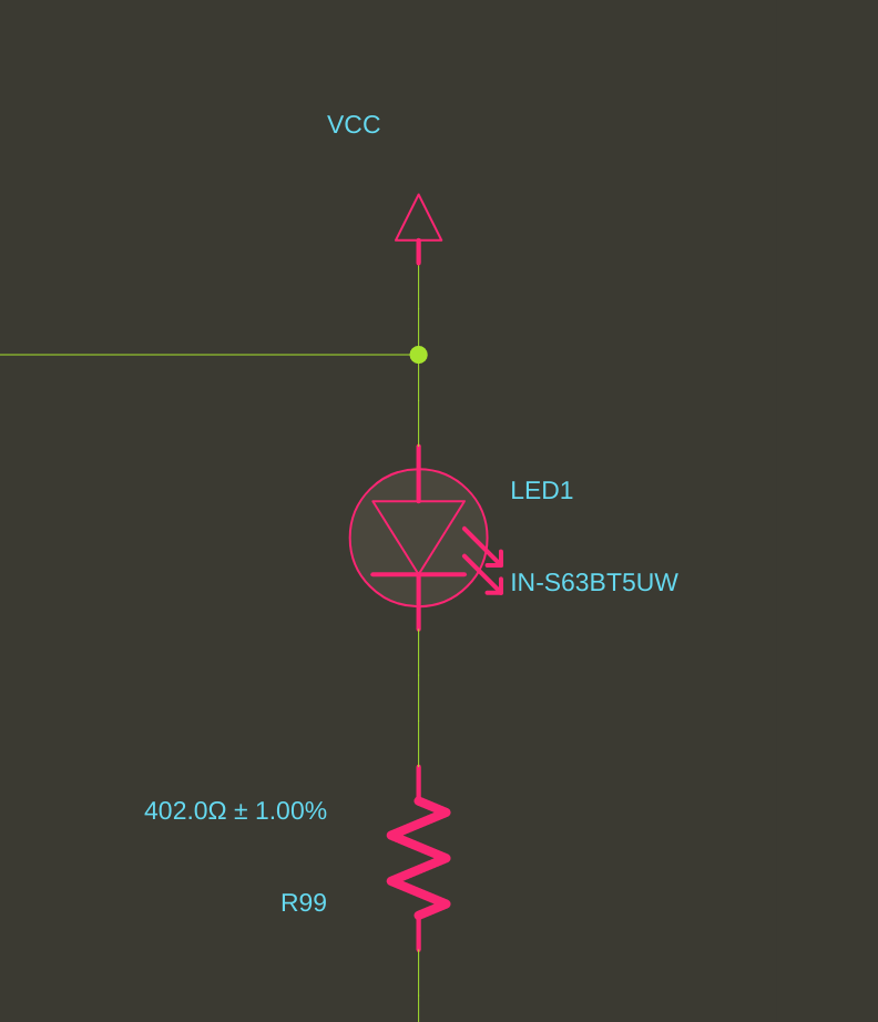 |  |
|---|
Edit a land pattern
Microcontroller U1 has silkscreen on all 4 corners, and we would like only silkscreen by pin 1. Let's delete the silkscreen on the other corners. In promicro.stanza we see inst U1 : atmega32u4-ep. Let's open atmega32u4-ep.stanza and search for silk. We want to delete all the corners that have 2 silkscreen lines and leave the corner that has 1 silkscreen line. If we are unsure, we can comment out the silkscreen we think we want to delete, save and reload. If the display looks correct, we can permanently remove them. Comment out code by highlighting it and pressing Ctrl+/
; layer(Silkscreen("F-SilkS", Top)) = Line(0.12, [ Point(3.62, -3.62), Point(3.62, -2.95) ])
; layer(Silkscreen("F-SilkS", Top)) = Line(0.12, [ Point(3.62, -3.62), Point(2.95, -3.62) ])
; layer(Silkscreen("F-SilkS", Top)) = Line(0.12, [ Point(3.62, 3.62), Point(3.62, 2.95) ])
; layer(Silkscreen("F-SilkS", Top)) = Line(0.12, [ Point(3.62, 3.62), Point(2.95, 3.62) ])
; layer(Silkscreen("F-SilkS", Top)) = Line(0.12, [ Point(-3.62, -3.62), Point(-2.95, -3.62) ])
; layer(Silkscreen("F-SilkS", Top)) = Line(0.12, [ Point(-3.62, -3.62), Point(-3.62, -2.95) ])
layer(Silkscreen("F-SilkS", Top)) = Line(0.12, [ Point(-3.62, 3.62), Point(-2.95, 3.62) ])
 |  |
|---|
Export the JITX Project to KiCad
Run export-cad()
The export backend defaults to KiCad.
Tip: More information on the export tool is in the JITX Reference - Export
Update the layout
When we bring a project from JITX to KiCad, it does not preserve the layout. This is simple to fix.
Copy the name of the generated kicad_pcb file and then delete it.
Copy the original kicad_pcb file into the new project folder.
Change the name of the kicad_pcb to the generated name.
Open the KiCad pro file. We should see a `kicad_pcb file in the project.
Open the kicad_pcb file.
Select Tools then Update PCB from Schematic...
Set the Match Method to Re-associate footprints by reference and check the Option to Update footprints
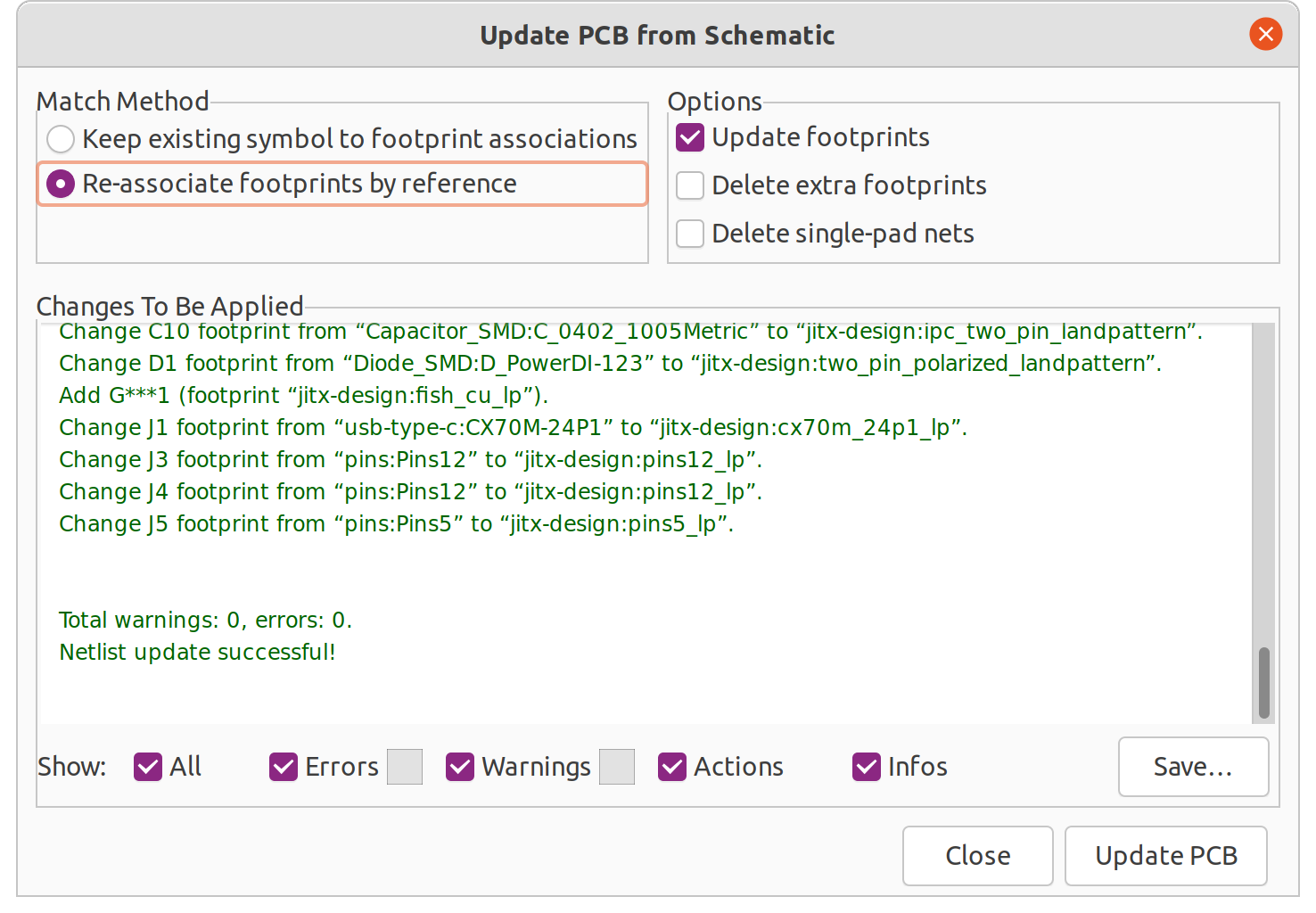
Press Update PCB
We should see the new parts we added. Also, due to the unusual reference designator of the Goldfish artwork, we may see that it moved.
We can now update the layout. We can either unroute the design and shrink the whole board, or we can make another development board and just recenter the tracks to the smaller components.
Rapid changes we can make in JITX
Our first design will be a development board we can order, and maybe our second design will be an even smaller board. We set the design rules for larger or smaller land patterns depending on what we're trying to accomplish. By changing one line of code, we can change all the passive components to be smaller size and the land patterns to be more dense. This will enable us to quickly go from development board to a packaged production design.
Development Board:
MIN-PKG = "0603"
DENSITY-LEVEL = DensityLevelA
Production:
MIN-PKG = "0201"
DENSITY-LEVEL = DensityLevelC
We can continue on this path and merge this board with another pcb-module to make a single, integrated board.
Summary
In this tutorial, we imported a design from KiCad, sourced alternate components for all of the capacitors and resistors, added a power LED circuit, and updated a land pattern. Simply by changing the resistor and capacitor calls, we went from a flat design that did not specify component part numbers, creating a lot of tedious work for us, to a stock-aware system. In other tutorials, we'll explore the additional benefits of software defined electronics.
Benefits:
- rapidly shrink the components on the board
- eliminate out of stock resistors and capacitors on the bill of materials and source in stock components
- specify only the important parameters
- quickly changed an evaluation board schematic to a production design
- improved land patterns
Revising an Existing Altium Design in JITX
This tutorial will walk through importing an existing design from Altium to JITX, modifying the design, exporting the design from JITX to Altium, and updating the layout.
You'll need:
- A licenced copy of Altium with the JITX extension installed
- An Altium project
Follow the steps in Install Altium JITX Extension before starting this.
This tutorial uses the Altium files for the STM32 Nucleo-64 development board - external link.
Sections:
- Import the Altium Project to JITX
- Make changes to the project
- Export the JITX Project to Altium
- Update the layout
- Rapid changes we can make in JITX
- Summary
Import the Altium Project to JITX
Follow the workflow outlined in Importing Altium to JITX to bring your project into JITX.
Make changes to the project
This project has several passive components that are out of stock and that we would like to replace with smaller components for a more integrated layout. It also has a series of jumpers, which we won't want in a more integrated project. There's a land pattern with silkscreen around one of the solder balls that will cause a manufacturing stoppage. We'll update the passive components for optimized checking, selection and sourcing. Remove connected jumpers and tie nets directly. And update the BGA land pattern.
These are some typical steps we may take when importing reference designs and using it in a different application.
We will make the following changes:
- Change the capacitors to generic, in-stock components
- Change the resistors to generic, in-stock components
- Remove jumpers and tie nets directly
- Update BGA land pattern
We will also open the generated file by pressing Ctrl+p and typing mb1367.stanza or double clicking on the file in the explorer window.
Open mb1367.stanza in VSCode, then go to File then Save As... and save it as motorcontroller.stanza. We'll make edits to this new file. Having the original file will be useful in case we want to do a file compare on our changes later.
We'll visualize the imported design by opening the output folder in VSCode and running from the VSCode terminal:
jitx repl motorcontroller.stanza
We can then rearrange our windows to see the generated code, the schematic, and the layout.
As we make changes, we can periodically test our code by saving
motorcontroller.stanzaand typingreloadat the stanza prompt.
We can see each schematic page is represented as a distinct box in the schematic viewer and in the stanza file as a schematic group. They are broken up into individual modules and called in the main pcb-module:
schematic-group(arduino_extension_connectors-submodule) = arduino_extension_connectors-submodule
schematic-group(mechanical-submodule) = mechanical-submodule
schematic-group(power-submodule) = power-submodule
schematic-group(st_link_v3e-submodule) = st_link_v3e-submodule
schematic-group(stm32_microcontroller_ios-submodule) = stm32_microcontroller_ios-submodule
schematic-group(stm32_microcontroller_power-submodule) = stm32_microcontroller_power-submodule
We can see the land patterns of each component in its location on the board.
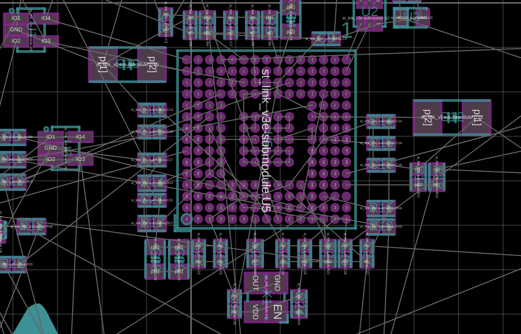
The import tool did not bring in the routing, because we don't need it yet. Later we'll bring the routing back in, and merge changes in a way that preserves traces and copper pours.
At the top of the file after our imports, we start with the power-submodule, which has 5 sections. The power-submodule corresponds to the schematic page titled Main power 5V / 3V3.
- Components are instantiated.
public inst ...The public statement means the component can be accessed outside of thepcb-module:
pcb-module power-submodule :
public inst C36 : mb1367/cc0402krx7r7bb104/MCD-00102/component
public inst C37 : mb1367/cc0603krx5r7bb105/MCD-00010/component
public inst C38 : mb1367/cc0805krx5r8bb106/MCD-00014/component
public inst C39 : mb1367/cc0603krx5r7bb105/MCD-00010/component
; ...
public inst SB5 : mb1367/rc0603jr-070rl/MCD-00071/component
public inst U11 : mb1367/ld1117s50tr/MCD-00088/component
public inst U12 : mb1367/ld39050pu33r/MCD-00215/component
public inst U14 : mb1367/tl1431cl5t/MCD-01802/component
- For each instance name, the component is assigned the reference designator name:
for inst in instances(self) do :
reference-designator(inst) = to-string(ref(inst))
- Component instances are placed at specific X, Y and rotations on either the
ToporBottomof the board.
place(C36) at loc(33.57, 47.24) on Top
place(C37) at loc(30.245, 45.615, 90.0) on Top
place(C38) at loc(17.47, 44.515, 270.0) on Top
place(C39) at loc(35.195, 44.365, 270.0) on Top
- Nets that connect the submodule to the rest of the board are exposed with
pin name:
pin p3v3
pin p5v
pin p5v_usb_chgr
pin p5v_usb_stlk
pin p5v_vin
- The internal netting is established:
net AGND (agnd, C46.p[1], C50.p[1], R34.p[1], U14.Anode)
net E5V (e5v, JP5.p[5])
net GND (gnd, C36.p[1], C37.p[1], C38.p[1], C39.p[1], C40.p[1], C41.p[1], LD3.p[0], U11.Gnd, U12.GND[0], U12.GND[1])
net NetC39_2 (netc39_2, C39.p[2], C40.p[2], SB5.p[1], U12.VOUT)
net NetC51_1 (netc51_1, C51.p[1], Q2.B, R35.p[1], U14.Cathode)
Change the capacitors to generic, in-stock components
By swapping capacitors with generic, in-stock components we:
- rapidly shrink the components on the board
- eliminate out of stock capacitors on the bill of materials
- and specify only the important parameters
We'll be able to change the minimum case size and use the sourcing tool to select only in-stock components.
We'll copy the component name cc0402krx7r7bb104 of the first capacitor, C36, and search for the component. It's 0.1 µF ±10% 16V Ceramic Capacitor X7R 0402 (1005 Metric). A search of the stanza file shows it's used 32 times in the design. Taking a look at the schematic, we can determine the highest voltage it's connected to is 5 Volts.
Let's replace all instances with a chip-capacitor() call.
I'll press Ctrl + H and initiate a find and replace. I'll select:
mb1367/cc0402krx7r7bb104/MCD-00102/component
And replace it with:
ceramic-cap(["capacitance" => 0.1e-6])
This will result in code calling instances of the chip capacitor function:
public inst C36 : ceramic-cap(["capacitance" => 0.1e-6])
; ...
public inst C40 : ceramic-cap(["capacitance" => 0.1e-6])
; ...
Since the maximum voltage on this board is 5 Volts (with the exception of Vin), We'll specify a project level minimum capacitor voltage of 10.0 volts, specifying a 100% headroom. We also specify a project level operating temperature. You can easily change inputs on a project level scale. If we're comfortable with less headroom, we can specify 6.3 Volts.
Right after the imports section of this file, We'll specify some project level parameters (note indentation):
import ocdb/utils/design-vars
OPERATING-TEMPERATURE = min-max(0.0 40.0)
OPTIMIZE-FOR = ["cost"]
MIN-PKG = "0201"
DESIGN-QUANTITY = 100
MIN-CAP-VOLTAGE = 10.0
This will select the cheapest capacitor that meets our specifications, 0201 or larger, with a minimum distributor stock to make my design, whenever a sourcing tool is called.
We can go through the rest of the design and replace capacitors in this manner. C41 connected to Vin need a higher min-rated-voltage since the Vin line can be up to 12 Volts. So I'll add "min-rated-voltage" => 25.0 to the capacitor function.
We can visualize resulting savings in board area from the original to using the generic cap call. We can also see the extra silkscreen is gone - land patterns match IPC-7352 density levels and have improved manufacturability.
| Original Capacitors |  |
|---|---|
| Generic Capacitors, MIN-PKG = "0201" |  |
| Generic Capacitors, MIN-PKG = "1206" |  |
This manner of specifying capacitors more accurately describes the design intent than just specifying a manufacturer part number. As electrical engineers, we can specify only the important parameters and JITX will select a component that meets or exceeds the parameters based on stock and what we are optimizing for. Knowing what the import properties of a part are helps an organization support the product through its entire life cycle.
Change the resistors to generic, in-stock components
Once we're done with the capacitors, we can go through the same steps with resistors.
By swapping resistors with generic, in-stock components we:
- rapidly shrink (or expand) the components on the board
- eliminate out of stock resistors on the bill of materials
- and specify only the important parameters
The first 2 resistors we encounter, R33 and R34, have a 0.5% tolerance and is used to set the reference voltage. We can specify the tolerance for these. The other resistors can have no tolerance specified, and we can optimize for cost.
public inst R33 : chip-resistor(10.0e3, 0.005)
public inst R34 : chip-resistor(33.0e3, 0.005)
public inst R35 : chip-resistor(180.0)
Remove jumpers and tie nets directly
This is a good time to check in our current status in our repository before going forward. In case we make a mistake, we can quickly revert to a working version.
We'll check in our code with:
git commit -am "Updated resistors and capacitors."
We're going to replace all the jumpers with net connections or leave them as opens. And, we'll comment out all the DNP components, enabling us to reduce BOM cost and shrink the board more.
To do this, we'll go through each pcb-module and compare it with the schematic page. The power module corresponds to page 6.
We will comment out SB5 (fitted) and SB14 (not fitted) by selecting each line and pressing Ctrl+/
Next, we will comment out the placements of each.
public inst R7 : chip-resistor(510.0)
; public inst SB14 : mb1367/rc0603jr-070rl/MCD-00071/component
; public inst SB5 : mb1367/rc0603jr-070rl/MCD-00071/component
public inst U11 : mb1367/ld1117s50tr/MCD-00088/component
...
place(R7) at loc(59.5, 70.85, 180.0) on Top
; place(SB14) at loc(48.59501, 24.19, 90.0) on Bottom
; place(SB5) at loc(37.97, 41.84, 90.0) on Bottom
place(U11) at loc(22.77, 43.615, 270.0) on Top
Finally, we'll modify the net statements (NetC51_2, VREF, NetC39_2, and p3V3 to connect the nets on each end of SB5 and remove references of SB5 and SB14.
Net p3V3 is modified to contain a reference to Net39_2.
net p3V3 (p3v3, JP6.COMMON, NetC39_2)
We will proceed the same way with the rest of the modules.
Update BGA land pattern
The microcontroller U5 land pattern has silkscreen around one of the BGA balls under the package and a big silkscreen box that could lift the component. We can see where the land pattern data for U5 is:
public inst U5 : mb1367/stm32f723iek6/MCD-00596/component
We can open up the file and search for silkscreen to find the silkscreen callouts. Then we can comment out the additional silkscreen. We will leave the two lines near pin 1 outside the box.
; layer(Silkscreen("F-SilkS", Top)) = Line(0.12, [
; Point(-4.25, 4.55),
; Point(-4.27283614024661, 4.66480502970953),
; Point(-4.33786796564404, 4.76213203435596),
; Point(-4.43519497029047, 4.82716385975339),
; Point(-4.55, 4.85),
; Point(-4.66480502970953, 4.82716385975339),
; Point(-4.76213203435596, 4.76213203435596),
; Point(-4.82716385975339, 4.66480502970953),
; Point(-4.85, 4.55),
; Point(-4.82716385975339, 4.43519497029047),
; Point(-4.76213203435596, 4.33786796564404),
; Point(-4.66480502970953, 4.27283614024661),
; Point(-4.55, 4.25),
; Point(-4.43519497029047, 4.27283614024661),
; Point(-4.33786796564404, 4.33786796564404),
; Point(-4.27283614024661, 4.43519497029047),
; Point(-4.25, 4.55)])
; layer(Silkscreen("F-SilkS", Top)) = Line(0.15, [Point(-5.075, -5.075), Point(-5.075, 5.075)])
; layer(Silkscreen("F-SilkS", Top)) = Line(0.15, [Point(-5.075, 5.075), Point(5.075, 5.075)])
; layer(Silkscreen("F-SilkS", Top)) = Line(0.15, [Point(5.075, -5.075), Point(5.075, 5.075)])
; layer(Silkscreen("F-SilkS", Top)) = Line(0.15, [Point(-5.075, -5.075), Point(5.075, -5.075)])
layer(Silkscreen("F-SilkS", Top)) = Line(0.15, [Point(-5.225, 5.225), Point(-4.325, 5.225)])
layer(Silkscreen("F-SilkS", Top)) = Line(0.15, [Point(-5.225, 4.325), Point(-5.225, 5.225)])
ref-label()
Export the JITX Project to Altium
Follow the workflow outlined in Exporting JITX to Altium to bring your project back into Altium.
Update the layout
When we bring a project from JITX to Altium, it does not preserve the layout. This is simple to fix.
Remove the generated PcbDoc from the project. Right click on the PcbDoc, and select Delete
Copy the original PcbDoc into the new project folder.
Open the PcbDoc in Altium.
Drag the PcbDoc into the project.
Save the project file.
In the PcbDoc, select import changes from design. Check the changes and deselect any you don't want to make.
Altium Tip: We set which changes we would like to import by right-clicking on project document, going to ECO Options, and changing the settings. Typically, we don't want to import changes that remove layout rules like net colors and impedance control. We can also edit default ECO options in the project options.
We can now perform layout work. We can either unroute the design and shrink the whole board, or we can make another development board and just recenter the tracks to the smaller components.
We can see that the trace connections to component pads need adjusting, since we have smaller capacitors now:

Rapid changes we can make in JITX
Our first design will be another development board, so we set the design rules for larger land patterns that can be hand reworked if needed and large passive components. By changing one line of code, we can change all the passive components to be smaller size and the land patterns to be more dense. This will enable us to quickly go from development board to a packaged production design.
Development Board:
MIN-PKG = "0603"
DENSITY-LEVEL = DensityLevelA
Production:
MIN-PKG = "0201"
DENSITY-LEVEL = DensityLevelC
We can continue on this path and replace power supplies and reference voltages with solvers, and merge development boards into a single, integrated board using pcb-module.
Summary
In this tutorial, we imported a design from Altium, sourced alternate components for all of the capacitors and resistors, removed several components, and updated a land pattern. Simply by changing the resistor and capacitor calls, we went from a flat design specifying specific components, which may be obsolete or out of stock, to a stock-aware system. In other tutorials, we'll explore the additional benefits of software defined electronics.
Benefits:
- rapidly shrink the components on the board
- eliminate out of stock resistors and capacitors on the bill of materials
- specify only the important parameters
- quickly changed an evaluation board schematic to a production design
- improved land patterns
Model a Land Pattern
Parametric Land Pattern Generation
In this tutorial you will learn how to create a standard land pattern parameterized by the design rules and design variables within JITX.
Example: TSSOP 20
Say we have a 20 pin thin shrink small outline package (TSSOP). The data sheet will look something like this:
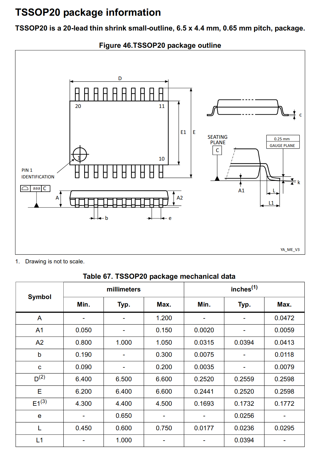
Within OCDB we can use the make-n-pin-soic-landpattern function to represent this component.
#use-added-syntax(jitx)
defpackage tssop20:
import core
import collections
import jitx
import jitx/commands
import ocdb/utils/landpatterns
public pcb-landpattern TSSOP20 :
make-n-pin-soic-landpattern(
20 ; number of pins
0.650 ; pitch, e in the table
min-typ-max(6.20, 6.40, 6.60) ; lead-span, E in the table
min-typ-max(4.30, 4.40, 4.50) ; package-length, E1 in the table
min-typ-max(6.40, 6.50, 6.60) ; package-width, D in the table
min-typ-max(0.45, 0.60, 0.75) ; lead length, L in the table
min-typ-max(1.9, (3.0 + 1.9) / 2.0, 3.0) ; lead width, b in the table
)
Now we can use this in a component.
#use-added-syntax(jitx)
defpackage STM32F031x4 :
import core
import collections
import jitx
import jitx/commands
import ocdb/utils/box-symbol
import tssop20
public pcb-component component :
name: "STM32F031x4"
pin-properties :
[pin: Ref | pads: Int ... | side: Dir]
[BOOT | 1 | Left ]
[OSC_IN | 2 | Left ]
[OSC_OUT | 3 | Left ]
[NRST | 4 | Left ]
[VDDA | 5 | Left ]
[PA[0] | 6 | Left ]
[PA[1] | 7 | Left ]
[PA[2] | 8 | Left ]
[PA[3] | 9 | Left ]
[PA[4] | 10 | Left ]
[PA[5] | 11 | Right ]
[PA[6] | 12 | Right ]
[PA[7] | 13 | Right ]
[PB[1] | 14 | Right ]
[VSS | 15 | Right ]
[VDD | 16 | Right ]
[PA[9] | 17 | Right ]
[PA[10] | 18 | Right ]
[PA[13] | 19 | Right ]
[PA[14] | 20 | Right ]
assign-landpattern(TSSOP20)
make-box-symbol()
Now that we have a component with a land pattern and symbol we can place it in a design
defpackage my-design :
import core
import collections
import jitx
import ocdb/utils/box-symbol
import jitx/commands
import ocdb/utils/defaults
import ocdb/utils/design-vars
import ocdb/manufacturers/rules
import stm32F031x4
pcb-module my-design :
inst mcu : stm32F031x4/component
place(mcu) at loc(0.0, 0.0) on Top
make-default-board(my-design, 4, Rectangle(10.0, 10.0))
view-board()
The visualizer shows us our generated component.
Parameterization
Under the hood the land pattern is parameterized by your design variables and design rules. We can see how the generated land pattern is altered when we change our design rules.
For example: in the previous screen shot the solder mask bridging may present an issue during manufacturing. We can choose a more precise manufacturing process for this design, and represent that by setting the corresponding design rules.
set-rules(sierra-circuits-notouch-rules)
make-default-board(my-design, 4, Rectangle(10.0, 10.0))
view-board()
The generated land pattern now appears to have wider solder mask bridges, due to the fact the design process has a tighter solder mask registration which is covered by the design rules.
You may also notice that the courtyard for this component is very tight - this is because the density level of our design is the highest by default. We can choose a less dense design, to contrast we'll use the least dense level, DensityLevelA.
DENSITY-LEVEL = LevelB
set-rules(sierra-circuits-notouch-rules)
make-default-board(my-design, 4, Rectangle(10.0, 10.0))
view-board()
Our generated land pattern now has a larger courtyard, and the heel/toe/sides of the pads has grown slightly as well.
Density levels and other design variables are documented here
Other land pattern types
There are many more land pattern generators, see the documentation for details.
Import Existing CAD Designs Into JITX
We can import designs from Kicad or Altium directly into JITX.
How to import Kicad designs into JITX
This tutorial walks through importing an open source project usb-sniffer into JITX. This project is available under a BSD 3-Clause New license which allows us to use the data with acknowledgement to Alex Taradov (https://github.com/ataradov). At the end of this tutorial, we will have experience using the KiCAD importer.
Tip: More information is in the command reference
Contents:
Create a new JITX project and set up for importing
Create a new directory in your filesystem named kicad-tutorial. This directory will be the root directory for the imported design.
Now use the New project command in the JITX sidebar of the VSCode extension to select the newly created (and empty) directory as the folder in which to create the project.
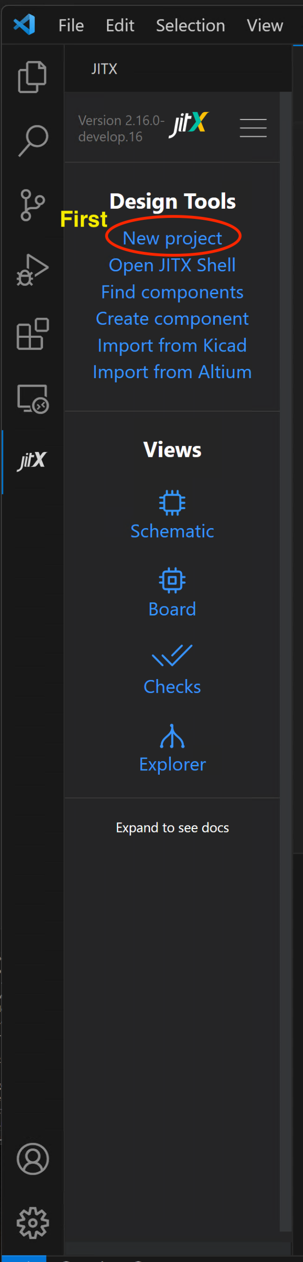
Let's add the Kicad project we want to import as a subdirectory of our new project directory. For this tutorial, we are going to use the usb-sniffer project as the starting Kicad project. Navigate to the git repository, download and unzip the repo using the Download ZIP option if you don't have git installed or git clone the repo into the project directory. For the git clone method, do the following:
cd kicad-tutorial
git clone https://github.com/ataradov/usb-sniffer.git
Delete the created files kicad-tutorial/main.stanza and kicad-tutorial/helpers.stanza as they are not needed for the imported project.
Our project folder now contains the following:
kicad-tutorial
\ usb-sniffer/
\ open-components-database/
| stanza.proj
Import project
Using the VSCode JITX extension, let's use the command to import a Kicad project Import from Kicad.
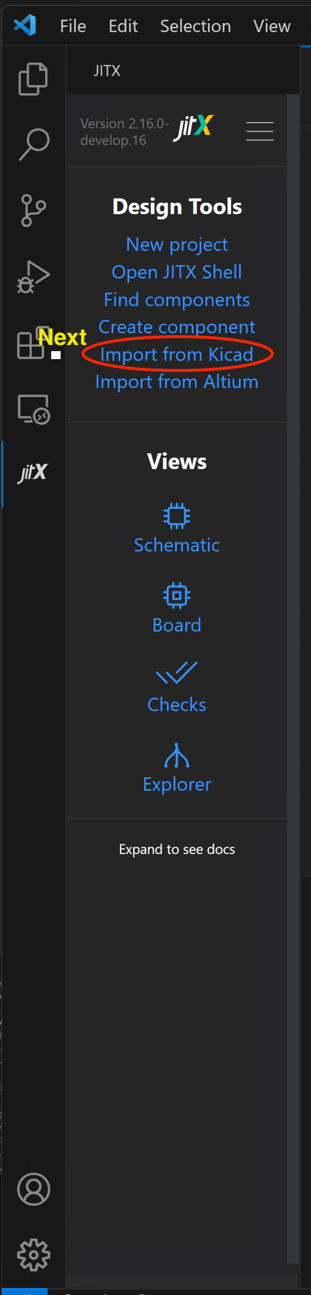
The file browser that appears is to choose the input Kicad project. Navigate to the usb-sniffer/hardware directory and press Choose as input directory.
The terminal window output alerts us to any issues and how the importer attempted to correct them. The log also describes those design elements that do not have a corresponding JITX construct. The log file is kicad-tutorial/kicad-imports/usb-sniffer/log.txt
A new directory, kicad-imports/usb-sniffer is created containing the imported design along with component and board data. usb-sniffer.stanza is the top level file of the new imported project. In order to run the design, the run-design.stanza file should be used.
Our project folder now contains the following:
kicad-tutorial
\ usb-sniffer/
\ open-components-database/
\ kicad-imports/usb-sniffer
| stanza.proj
To compile the imported usb-sniffer project, we now open the run-design.stanza file. We need to edit this file in order to successfully run the project. The changes are:
- Add a new package for default board design rules.
- Near the top of the file, insert the line
import ocdb/manufacturers/rulesafter the lineimport ocdb/utils/defaults
- Near the top of the file, insert the line
- Update the design rules for the board.
- Edit
run-design.stanzaand replace the line that saysset-rules(design-rules)withset-rules(jlcpcb-rules
- Edit
Then, press "Ctrl+Enter" - and JITX will compile and run the imported project. You can open the schematic, board and design explorer views by using the buttons in the JITX extension.
Next Steps
The KiCad design is now in JITX. Next, let's edit the imported JITX project to use the more advanced features of JITX in the Revising an Existing KiCad Design in JITX tutorial.
Notes
The imported components will have their (X,Y) locations imported in the tool in the form of:
place(self.BAT54S) at loc(-15.2019, 14.1859, 270.0) on Bottom
Once the component is placed in code like this, the component is considered locked and will not be moveable in the board view. If you want to move the component in the board UI, you will need to delete the place() statement in the code.
If we are designing a mating PCB, we can use this same notation with the same locations to place mating components in JITX.
Keeping the reference designators the same is an important method to be able to keep our layout when we make revisions. It is accomplished by:
for inst in [<xxx>] do :
reference-designator(inst) = to-string(ref(inst))
If we wish to name your instances something more descriptive, we can set reference designators manually with:
reference-designator(instname) = "U1"
Any instance without an assigned reference designator will get one assigned automatically.
Optional: Attach BOM data
JITX supports importing BOM data for manufacturer names and manufacturer part numbers (MPN) in imported pcb-components. This feature requires generating a jitx-import-bom.tsv in the import data directory.
See the BOM Data Format Reference to see how the data should be structured.
Errata
See the Kicad Importer Errata for current known issues with projects imported from Kicad.
How to import from Altium Designer into JITX
Prepare an Altium Project for Import
If you have not installed the Altium extension, follow the instructions for Installing the JITX Altium Extension. JITX and Altium should be installed on the same computer and able to launch at the same time.
Before importing Altium data to JITX, make sure you've done the following :
- Open Altium and be sure to activate a valid Altium license.
- Make sure all parts are in both the schematic and layout, they must not be missing in either!
- Make sure the schematic is fully annotated. No
?characters in reference designators are allowed. - Synchronize designs by running
Update board from schematicfrom Altium. - Ensure only one
.PcbDocis associated with the Altium project you are trying to import. - Get better component data, using a
jitx-import-bom.tsvfile.
Import the prepared design
Either create a new project in JITX or open an existing project folder in VS Code.
In the JITX pane in the extension, select "Import from Altium", and browse to the PrjPCB file for the project you prepared in the first step.
JITX generates code for the design and the components for the Altium project we just imported in the altium-imports directory. We can now use our design data in JITX!
Structure of the imported design
The JITX importer generates code from the source Altium project. The code is structured to be as reusable as possible, and tries to translate the structure in the schematic into reusable circuits. Enough data is maintained to allow reproduction of the original design in Altium.
Files
Let's say we import an Altium project named RedOctober. The importer will then generate the following directory:
RedOctober/
symbols/
landpatterns/
components/
3d-models/
RedOctober.stanza
reference-designators.stanza
properties.stanza
placements.stanza
labels.stanza
board.stanza
run-design.stanza
log.txt
stanza.proj
symbols/ This directory contains symbols that are used more than once by components in the design.
landpatterns/ This directory contains landpatterns that are used more than once by components in the design.
components/ This directory contains component models for the parts in the design. It is organized by manufacturer.
3d-models/ This directory contains the 3D models present in the design.
RedOctober.stanza This file contains the JITX version of the original design. The design is composed of a tree of pcb-modules in order to get the most reusability:
- the
mainpcb-module is the top-level design. Running this module will re-create the original designpcb-module maininstantiates other pcb-modules for each schematic sheet in the project.- Each of those
schematic-sheetlevel modules instiates pcb-modules for each group of symbols that are directly wired together. So we should usually get each individial circuit in our design coming in as a reusable pcb-module. This is not perfect, and it's normal to rearrange these modules a bit to get a great heirarchical and reusable representation of our design.
reference-designators.stanza This file sets the reference designators of the components in the design so that the original design can be regenerated.
properties.stanza This file contains the Altium parameters stored as JITX properties.
placements.stanza This file contains the component placements from the board.
labels.stanza This file sets the detailed size and location of reference and value labels so the original design can be recreated.
board.stanza This file contains material and stackup definitions, as well as the board outline geometry.
run-design.stanza This file contains commands to run the main module defined in RedOctober.stanza either to run checks or re-export the design to Altium.
log.txt This file is a log of the import, noting data inconsistencies in the source design file and how they were handled.
stanza.proj This file links all of the above stanza files mapping package definitions to the file that contains them.
Custom Layer Names
Mechanical layers in Altium will map to the CustomLayer instances with the name Pcb-Mechanical## where ## maps to the number of the mechanical layer.
Other special layers such as:
Pcb-DrillDrawing
Pcb-MultiLayer
Pcb-ConnectLayer
Pcb-BackGroundLayer
Pcb-DRCErrorLayer
Pcb-HighlightLayer
Will also map to a string representation.
Errata
See the Altium Importer Errata for current known issues with projects imported from Altium.
Export JITX Designs To CAD
We can export JITX designs to Kicad or Altium.
How to export from JITX into Altium Designer
We can export a JITX design to an Altium project that includes a .pcbdoc, a .schdoc, as well as a .pcblib and .schlib.
NOTE: Our extension is verified to work for Altium versions 18 through the latest version 22.8.
If you have not installed the Altium extension, follow the instructions for Installing the JITX Altium Extension. JITX and Altium should be installed on the same computer and able to launch at the same time.
Set up export-cad
We configure an export to Altium in our program by first creating a new design in JITX. Then, add the following code to the end of your main.stanza file.
set-main-module(my-design)
val board-shape = Rectangle(10.0, 10.0)
pcb-board my-circuit-board :
stackup: my-stackup
boundary: board-shape
signal-boundary: board-shape
layer(Silkscreen("F-silk", Top)) =
Text("Board v1.2.3", 2.54, C, loc(0.0, 0.0))
set-board(my-circuit-board)
set-current-design("jitx-design")
set-export-backend(`altium)
set-use-layout-groups()
export-cad()
set-current-design("jitx-design") This sets the directory where our Altium project will be created
set-export-backend(`altium) This specifies that Altium should be used for export.
set-use-layout-groups() This defines that components should be grouped in the generated layout by layout-group.
export-cad() Run the exporter.
Open Altium and run the design
Launch Altium, activate a license, and close all documents.
In JITX, run a generator that includes the export functions defined above.
The extension will read in your file and build an Altium project for you. Do not touch anything in Altium while the files are being generated. A large design may take a couple of minutes, and you'll see messages appear in the status bar in the lower left corner of the screen.
After the Altium project is created, synchronize the schematic and layout to finalize the new project.
Running DRC
See Altium DRC errors in the known issues for further steps on running Altium DRC on an exported design.
How to Install the JITX Extension for Altium Designer
The JITX Extension for Altium Designer is automatically installed if the prerequisites are met.
Prerequisites:
- Windows
- Altium Designer (installed, but not running)
- JITX
NOTE: Our extension currently works for Altium versions 18 through the latest version 22.8.
Automatic Installation
Once the prerequisites are met, the installation of the extension is triggered the first time you:
- Open VSCode while being already signed in
- Sign in to JITX within VSCode.
Manual Installation
You can also install the JITX extension for Altium via the menu at the top right-hand corner of the JITX Sidebar in VSCode.
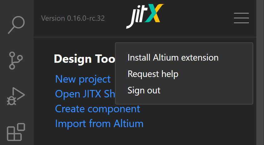
How to export from JITX into Kicad
We can export a JITX design to a Kicad project that can be opened immediately in Kicad 7.
Before you start, make sure you have Kicad 7 installed.
Set up export-cad
We configure an export to Kicad in our program by first creating a new design in JITX. Then, add the following code to the end of your main.stanza file.
set-main-module(my-design)
val board-shape = Rectangle(10.0, 10.0)
pcb-board my-circuit-board :
stackup: my-stackup
boundary: board-shape
signal-boundary: board-shape
layer(Silkscreen("F-silk", Top)) =
Text("Board v1.2.3", 2.54, C, loc(0.0, 0.0))
set-board(my-circuit-board)
set-current-design("jitx-design")
set-export-backend(`kicad)
set-use-layout-groups()
export-cad()
set-current-design("jitx-design") This sets the directory where our Kicad project will be created
set-export-backend(`kicad) This specifies that Kicad should be used for export.
set-use-layout-groups() This defines that components should be grouped in the generated layout by layout-group.
export-cad() Run the exporter.
Custom Layer Mapping
Currently, the CustomLayer geometry is exported using two mappings.
Static Mapping
CustomLayer Layer Name | Kicad Layer Name |
|---|---|
| "Drawings" | "Dwgs.User" |
| "Comments" | "Cmts.User" |
| "Eco1" | "Eco1.User" |
| "Eco2" | "Eco2.User" |
| "Margin" | "Margin" |
| "Fab" | "Fab" |
Other Custom Layers
Any other custom layers are mapped in order of appearance to the layers User.2, User.3, User.4, ..., User.8. Any custom layers beyond User.8 are all flattened into User.9.
Open Kicad and run the design
Launch Kicad.
In JITX, run a generator that includes the export functions defined above.
A ready-to-use Kicad project will be generated for you in the "CAD/kicad" directory. Open this project. You've now imported a JITX design into Kicad!
When You Don't Know How To Do Something in JITX
While designing a board in JITX, you'll often come to a point where's something that you want to do, but you don't know how to do it in JITX. Below is a suggested workflow when you're "stuck":
- Search the JITX Documentation
- Search OCDB
- Checkout the JITX Cookbook Example Projects (Recipes) and check if any of the examples do what you're trying to do.
- Reach out for help:
- Ask your question in the JITX Slack
- Submit a ticket: https://support.jitx.com/hc/en-us/requests/new
JITX Essentials
Design Hierarchy
In JITX, we can think of an electronic circuit as a hierarchical graph of components and modules. We call this graph the circuit graph. Understanding the circuit graph is critical to understanding how the code, schematic, and board work together in a complete design.
This hierarchical graph concept is a pretty common trait in many CAD tools. Just to name of few:
- Tools like Unity and Blender use a Scene Graph to arrange models, cameras, and other objects.
- Solidworks uses a Design Tree for capturing the relationships between components and assemblies.
Most ECAD tools have this kind of hierarchical graph as well but the schematic capture tools can make it a bit more opaque.
- For many tools, each schematic sheet is an implicit "module" of the design.
- Multiple sheets are combined together to form a complete design.
- Multiple circuits might end up on one sheet that might otherwise be better off as independent modules.
- Coming from Altium, you will probably be familiar with multi-channel hierarchical designs.
Modules
The circuit graph consists of two main types of nodes:
- Module nodes - pcb-module - can be thought of as sub-circuits.
- Component nodes - pcb-component - represent physical or virtual electronic components.
Note, that we're not using circuit here in the graph theory definition of the word circuit -- more in the "Sparkies make electrical circuits" definition of the word circuit.
FPGA Designers - The following will likely feel pretty familiar to you. Whether you are coming from VHDL, Verilog, or others, the modular structure of a design in JITX will mimic the structural architecture of many HDL designs.
Instances and Instantiables
Each of the pcb-module or pcb-component statements in a design can be thought of as the definition for a sub-circuit or component, respectively. We call these Instantiable types. Each Instantiable can be processed to form an Instance type. The Instantiable is the recipe and the Instance is the rich chocolate soufflé made from that recipe.

The root node of the circuit graph will always be an instance of a pcb-module. The root node will be the parent of any number of child nodes, be they pcb-module instances or pcb-component instances. The pcb-component instances are always going to be leaves of that tree - they will never be the parent of any other instances.
Instances are constructed inside a pcb-module with the inst statement:
pcb-component NE555:
...
pcb-module top-level:
inst timer : NE555
; ^^^^------------------- JITX Keyword for Instantiation
; ^^^^^------------- Symbol Name of the constructed Instance
; ^^^^^----- Instantiable (recipe) for this Instance
Here we construct an instance of the NE555 Instantiable. In this example, NE555 is a component, but it could just as easily have been a module. The instance is named timer which is a symbol in the top-level module context.
InstanceTypes
When constructing an Instance from an Instantiable, each instance can be one of 3 types:
SingleComponent- An instance constructed from apcb-componentSingleModule- An instance constructed from apcb-moduleInstanceArray- An array of instances constructed from eitherpcb-componentorpcb-moduledefinitions.
To determine what type a particular symbol is, we would call the instance-type function. In the previous NE555 example, calling instance-type on timer would return SingleComponent
InstanceArray
In the previous NE555 example - we constructed a SingleComponent instance. To construct an InstanceArray type, we would add a [...] suffix:
pcb-component NE555:
...
pcb-module top-level:
inst timers : NE555[4]
; ^^^^-------------------- JITX Keyword for Instantiation
; ^^^^^^------------- Symbol Name of the constructed Instance
; ^^^^^----- Instantiable (recipe) for this Instance
; ^^^-- Instance Array Parameters
In this example, we construct an InstanceArray type of instance. In this case, the array contains 4 distinct SingleComponent instances of the NE555 Instantiable. This array functions similar to an array in C with zero-based indexing.
val symb-type = instance-type(timers)
println("Array: %_" % [symb-type])
val elem-type = instance-type(timers[0])
println("Single: %_" % [elem-type])
; Prints:
; Array: InstanceArray
; Single: SingleComponent
Attempting to access an InstanceArray with a negative index or an index outside the arrays bounds will result in an exception.
Labeling the Circuit Graph
As we peruse the circuit graph, we need a way to uniquely label instances at arbitrary depth in the graph. We accomplish with a . (dot) notation similar to attribute notation in Python. Let's say we have a hypothetical instance audio in our current context:
audio.pre-amp[1].op-amp.vout
This line demonstrates a dot-path label that uniquely identifies a particular object. For example, this label might indicate the following structure:
- audio => Module
|
-- pre-amp[0] => Module
| |
| -- op-amp => Component
| |
| -- vout => Pin
|
-- pre-amp[1] => Module
|
-- op-amp => Component
|
-- vout => Pin
...
dot notation combined with array indexing allows us to uniquely identify every module, component, pin/port, etc in the circuit graph.
These dot notation strings are called refs.
Acyclic Circuit Graph
The circuit graph is primarily a means of describing the "ownership" of component and modules nodes. It is not describing the interconnection between components or modules.
Because this graph is describing hardware, there are no cycles in this graph. In other words, the circuit graph is acyclic. Again - this is not suggesting that the net list is acyclic - only the circuit graph. Cycles in the net list or component connections are of course possible for things like feedback, oscillators, etc.
Example - Invalid Circuit with Cycle
pcb-module A :
inst U : B
pcb-module B :
inst W : A
pcb-module top-level:
inst Z : A
In this example, The module A instantiates module B and vice versa. This creates a cycle and this is not allowed.
Modules in the Schematic
The circuit graph plays an important role schematic visualization as well.
Each pcb-module has an implicit schematic-group statement. All of the child component/sub-module instances of a module are added to that schematic group by default. This implicit, per-module schematic group provides a reference point - dare we say, a grounding - between code text and visual schematic medium.
Schematic groups are method of organizing our schematic sheets with like circuits. They also provide a natural boundary between circuits that are not intended to interact.
In the image above, notice that the schematic groups are labeled with the same dot notation labeling as the modules. This makes it mapping the schematic groups to the code easier for debugging.
Introspecting the Circuit Graph
Once constructed, it is often useful to walk this graph to inspect parts of the circuits, add checks, or make connections in an automated way. There are several functions that support this kind of introspection:
These functions are variations on same concept - they allow us to iterate through the children of a pcb-module. The important thing to note is that they are not recursive(!). They will only provide references to the direct children of the passed instance.
Example - Recreating component-instances
As a beginning exercise, we can recreate the component-instances function in pure stanza:
public defn my-component-instances (mod:JITXObject|Instantiable) -> Seq<JITXObject> :
generate<JITXObject>:
for child in instances(mod) do:
if instance-type(child) is SingleComponent:
yield(child)
Example - Recursive Instances
Note - This is a more advanced example with recursion. Fear not brave electro-adventurer - These examples will serve you well as you become more comfortable with the JITX Environment.
doc: \<DOC>
Generate a recursive sequence of all child components/modules
This function expands `InstanceArray` by serving each individual
instance as an element in the returned sequence.
<DOC>
public defn instances-rec (mod:JITXObject|Instantiable) -> Seq<JITXObject> :
generate<JITXObject>:
for child in instances(mod) do:
match(instance-type(child)):
(s:SingleComponent|SingleModule): yield(child)
(a:InstanceArray):
for i in instances-rec(child) do :
yield(i)
In this function, we can pass either a module instance (JITXObject) or a module definition (Instantiable) and this function will produce a
sequence of JITXObject instances.
This function uses a stanza generator construct which is similar to Python generators.
Notice that this example uses a match statement instead of an if/else clause like the previous. This is a common, idiomatic pattern in Stanza.
The type SingleComponent|SingleModule matches on either SingleComponent or SingleModule
Because the graph is acyclic, we are guaranteed that this recursive function will exit.
Example Designs - The JITX Cookbook
The JITX cookbook is a number of systems that we have designed, implemented, and manufactured in JITX. These example projects can serve as reference designs or a template for your next project. Visit the JITX Cookbook repository for a detailed walkthrough of all of the recipes.
Recipes
Click any of the links below to access a detailed walkthrough of how they were designed in JITX.
| Recipe | What It Can Do |
|---|---|
| Battery Charger | LiPo battery charger, LDO volgate regulator, USB-C connector, JST battery connector, resistors, capacitors, detailed checks, export to KiCad |
| USB-C Cable Tester | Test points, programmatic parts placement, USB-C connectors, LEDs, coin cell battery, circuit introspection |
| BLE-mote Wireless IOT Sensor Board | Microcontroller, pin assignment (supports/requires), parametric design, design optimization, copper pour, net-classes, stackup |
| Hacking Conference Badge | A software-defined electronics playground - learn JITX by designing your own conference badge |
Frequently Asked Questions
How do I find more information on…
docs.jitx.com is the main source of documentation on the JITX language and IDE.
Also see: Tips For When You're Stuck
What do I do when I'm stuck / can't figure out how to do something?
See: Tips For When You're Stuck
How do I compile a design?
You can compile a design by:
- Have VSCode open in a folder that has a stanza.proj file linking the design. Open the file in VSCode and press <Ctrl> + <Enter> to run the design in the JITX Shell.
- Call the JITX executable directly with the file. e.g.
/path/to/.jitx/jitx repl my-file.stanza. (<Ctrl> + <Enter> is a shortcut for this operation)
How do I check my design?
Try the Check a design tutorial to learn how to check designs in JITX.
How do I export data?
Top Level Commands describes export-cad and export-bom to export CAD and bill of materials data.
You can also write scripts in JITX to collect, transform, and export any data you want.
How do I import data?
Top Level Commands describes import-cad for bringing in existing CAD data. It's also common to write one-off importers for things like bump-maps or FPGA constraint files. These typically read the source data and emit JITX code that can be run as part of a design.
How do I edit the schematic? The layout? The symbols?
The best way to edit a schematic in JITX is to organize it by following the Organize a schematic tutorial.
You can pre-place components in the layout using loc statements to hard-code geometric constraints. If you place components in a module, and then use that module in a design, remember to place the module too. Typically we only pre-place things that actually need to be fixed, then leave it to the solvers, and finish ourselves in CAD.
Symbols are defined in JITX code. You can import them, define them yourself, or use the pre-defined symbols in ocdb/utils/symbols.
How do I instantiate a component?
inst c : my-component
How do I import or use a library?
You can import existing CAD designs to create libraries of JITX code (see the guide How to import from Altium).
To use a library of JITX code, edit the stanza.proj file in your active project to include a line like include "../path/to/library/stanza.proj. Everything linked by that stanza.proj file can now be used in your project.
How do I create or manipulate geometry?
Outside of pads in a landpattern, layout geometry can be created with geom statements for conductive elements, and layer for non-conductive things.
How do I report a bug?
From the menu in the JITX extension pane, click Report a bug.
How do I find more components?
You can test search your JITX libraries for keywords, and query the component database for large-scale searches: Part Query API
How do I get an area estimate?
When you run view-board() for your design, the placer will show you a dense layout of your components so you know the overall size of the design.
How do I optimize pin assignment?
Pin assignment is not optimized for routability yet (being worked on now - it'll be great!). To lock in specific preferences for pin assignments, directly net pins instead of using support statements. e.g.
net (stm32.PA[4] sensor.i2c.sda)
net (stm32.PA[5] sensor.i2c.scl)
Instead of
require i2c:i2c from stm32
net (sensor.i2c i2c)
How do I use a STM32 microcontroller?
We have 1500+ STM32 microcontrollers in our component database. designs/mcu.stanza in the open components database shows how to query for microcontrollers based on parameters like which STM32 series you want to use.
How do I use a ESP32 microcontroller?
The ESP32-PICO-D4 is modeled in the open components database, and you can also look to designs/ble-mote.stanza as an example design using the ESP32.
How do I share my JITX design with another user?
A JITX design is code, and you can share it like you share any other file. We usually keep the code for a project checked into a Git repository, which makes for easy collaboration on JITX designs and generators.
Are PCB objects positioned globally or relatively to each other?
By default, when you assign a position to an instance in a module it's in a global frame associated with that module. You can create relative poses using the relative-to keyword in a loc statement. loc docs.
What is a stanza.proj file and how do I use it?
stanza.proj files are used to link your JITX code together. They contain pointers to which packages are defined where. For example in ocdb, the stanza.proj file for TDK components contains:
package ocdb/components/tdk/MPZ1608 defined-in "MPZ1608.stanza"
For example the root level stanza.proj brings in the file mapping TDK components:
include "components/tdk/stanza.proj"
How do I add a component to OCDB?
Fork the open source repository and create a pull request. This is a great way to get feedback on your code while contributing back to the community.
How do I check the current working directory in the JITX Shell?
The utils/file-system package has a helper function for returning the current working directory as a String.
import utils/file-system
println(get-cwd())
How do I fix Error loading webview errors?
There is a known bug in Visual Studio Code that causes the following error message :
Error loading webview: Error: Could not register service workers: InvalidStateError: Failed To Register a ServiceWorker: The document is in an invalid state.
This error occurs happens when Visual Studio Code updates itself automatically and is not unique to JITX. It can be tracked here :
Workarounds :
A workaround is to kill any running VSCode processes and restart.
Linux and MacOS
pkill code
Mac OS
Open Task Manager, locate any running instances of VS Code, and force kill them.
(Optional) Disable Auto Updates
This error usually occurs after an update of VS Code. To prevent it from arising, you can disable auto updates.
Installation Instructions for the JITX App
This page walks you through the steps to install and log in to JITX.
Before using JITX, you must set up your JITX account -- instructions have been sent via email.
JITX is shipped as an extension for VS Code. Therefore, we first install VS Code and then add the JITX extension for VS Code.
Steps:
1 Install Visual Studio Code
The JITX compiler and UI are integrated with VS Code. VS Code is an integrated development environment (IDE) which integrates tools for development including an editor, compiler, and source control. To install VS Code:
- MacOS
- Linux (For Ubuntu use:
sudo apt-get install code- do not use snap, which installs an old version) - Windows (we can also install from Microsoft store)
2 Install the JITX VS Code Extension
There are two ways to install the JITX VS Code extension.
Method 1: Install from the Visual Studio Marketplace
Follow the instructions from the marketplace: While in VS Code, Ctrl-P, enter ext install JITX.jitpcb-vscode in the text box and then press Enter to install the JITX VS Code extension directly.
Method 2:
Click the Extensions icon ![]() in the Activity Bar, search for "jitx" and install it.
in the Activity Bar, search for "jitx" and install it.
3 Open the sidebar
Click on the JITX icon in the left hand activity bar to open the JITX sidebar.
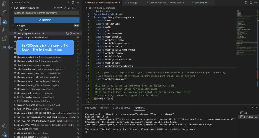
4 Login to JITX
Click the JITX icon ![]() in the Activity Bar and sign in with the username and password you created using the link from the welcome email.
in the Activity Bar and sign in with the username and password you created using the link from the welcome email.
That's it! You're ready to start designing circuit boards in JITX. Next section: Your first JITX design
Troubleshooting your JITX installation
This section details how to troubleshoot possible issues with the installation process.
1. JITX is not on your PATH
jitx: command not found
Add JITX to the PATH variable:
export PATH="~/.jitx/current:$PATH"
In Mac and Linux, add the above line to your environment configuration file (~/.bashrc, ~/.zshenv), and close/reopen all terminal windows, including terminals in VSCode, for the change to persist.
In Windows, type setx PATH "%PATH%;%USERPROFILE%/.jitx/0.11.2/ (replace 0.11.2 with the version on your machine) in the terminal.
Verify JITX is now in your PATH:
$ jitx
Expected a command name.
2. Verifying that your JITX installation is not corrupted
Run jitx check-install to validate that the program matches your system.
$ jitx check-install
installation-type: release
installation-dir: /home/mikedorf/.jitx
version: 0.11.2
target: ubuntu-bionic
current-target: ubuntu-bionic
3. Manual Installation
In the event that installation through VS Code cannot be completed, you can install the software manually.
Download the Software
Extract the launcher and run the installer
unzip -j jitx.zip "jitpcb.release/jitx"
./jitx install-from-zip
rm jitx jitx.zip
Known Issues
Error Opening Webview :
This is a bug in Visual Studio Code.
Closing VS Code and killing the process by running
pskill code
And reopening VS Code may fix the issue.
Keyboard Shortcuts / Hotkeys
JITX has a plethora of built-in keyboard shortcuts (also known as hotkeys) which make it very quick to move around in and modify your schematic and physical design.
Both the schematic and physical design views have built in help ("?") buttons that will expose a list of every available keyboard shortcut. Clicking this "?" button in the schematic and physical design views is the best way to get info on available hot keys while designing your PCB.
Here is the button to access hotkeys, this will be available in the schematic and physical design windows after you compile a design and run view-board() and view-schematic():

Reference - Keyboard Shortcut / Hotkeys
We reccomend using the built-in views to find the latest hotkeys, but we've also included a reference below:
Schematic:
Physical Design: