

JS5: Diplexer from Spec#
Shortcut: Download the runbook, save it beside
the vendor files it lists, give them to your AI coding agent, and tell it to follow the file.
Design a diplexer for 2.4 to 2.5 GHz and 5.1 to 5.9 GHz that beats the Mini-Circuits ZDPLX-592-S+, by prompting an agent that drives the JITX HFSS optimization skill. The agent sizes the filter from closed-form design, builds a 2-layer RO4350B board for JLCPCB in JITX, tunes the SMA launch, then runs an HFSS campaign on the whole board. You approve the rough path and the simulation setup, and set the budget.
What you learn is how to take an RF requirement to a fab-ready layout through a full-wave optimization loop that the agent runs and you steer.
What one run produced#
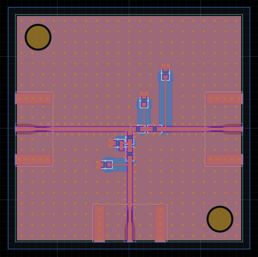
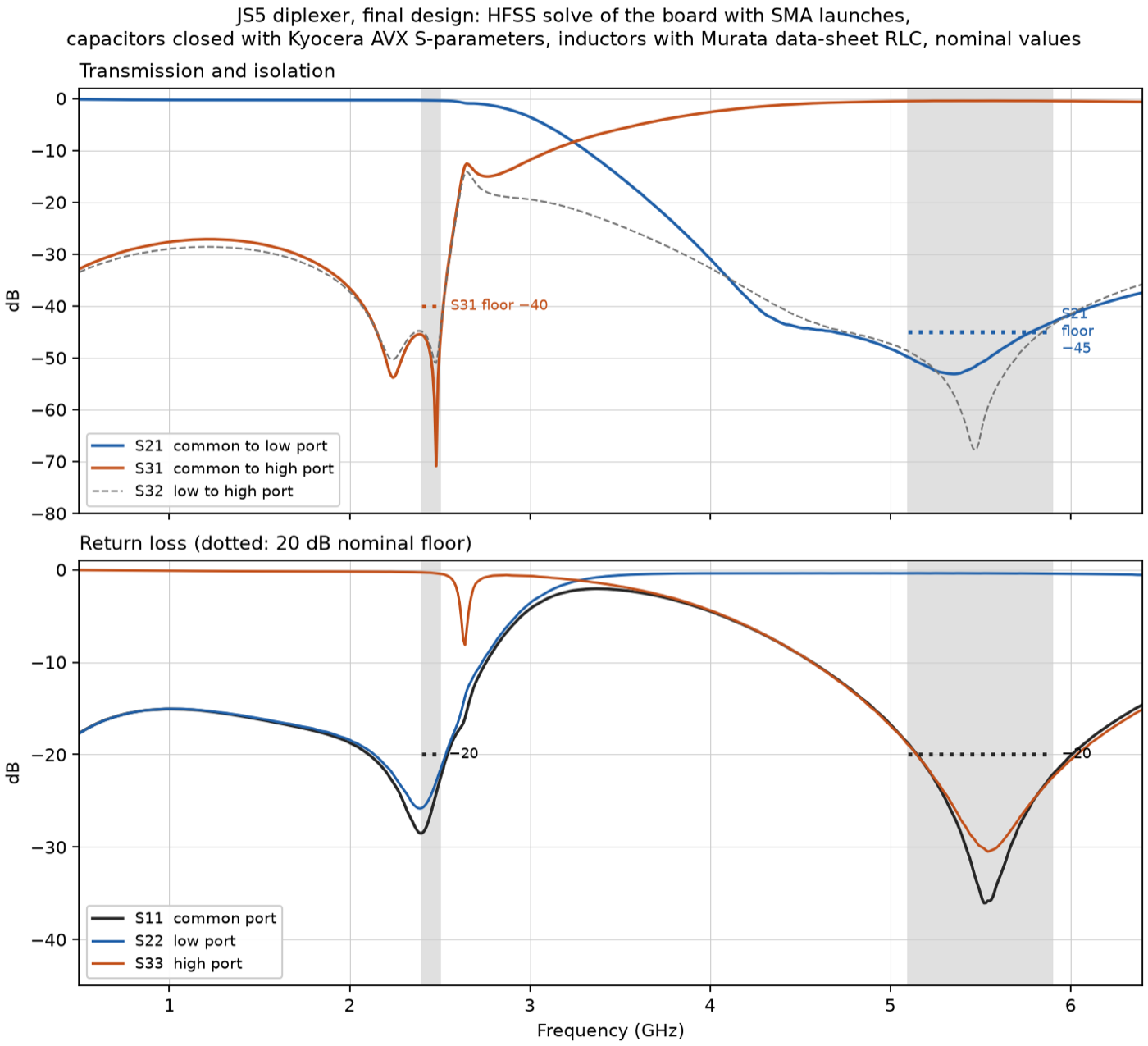
One run, on earlier revisions of the runbook, produced the board below. Simulated at the SMA connectors, it beats the ZDPLX on every specification but one: low-port isolation is 43.1 dB at nominal against the ZDPLX’s 45 dB typical. Worst-corner insertion loss is 0.33 dB under the ZDPLX typical on the low port and 0.35 dB under it on the high port. The runbook sets some targets tighter than the ZDPLX on purpose, to push the agent; the run met 12 of its 16 floors, and the table compares with the ZDPLX itself.
Metric |
Band (GHz) |
ZDPLX typical |
Board, nominal |
ZDPLX min or max |
Board, worst corner |
|---|---|---|---|---|---|
Insertion loss, low port |
2.4 to 2.5 |
0.8 dB |
0.42 dB |
≤ 1.2 dB |
0.47 dB |
Insertion loss, high port |
5.1 to 5.9 |
0.9 dB |
0.52 dB |
≤ 1.7 dB |
0.55 dB |
Return loss, low port |
2.4 to 2.5 |
16 dB |
21.8 dB |
≥ 10 dB |
18.0 dB |
Return loss, high port |
5.1 to 5.9 |
12 dB |
19.0 dB |
≥ 8 dB |
17.4 dB |
Return loss, common port |
2.4 to 2.5 |
16 dB |
22.8 dB |
≥ 10 dB |
18.8 dB |
Return loss, common port |
5.1 to 5.9 |
12 dB |
18.8 dB |
≥ 8 dB |
17.1 dB |
Stop-band isolation, low port |
5.1 to 5.9 |
45 dB |
43.1 dB |
≥ 38 dB |
41.2 dB |
Stop-band isolation, high port |
2.4 to 2.5 |
40 dB |
45.5 dB |
≥ 35 dB |
41.7 dB |
Each metric’s worst corner is set by the parts’ tolerance and temperature drift. No board has been fabricated yet; one will be. The scored board had its in-pad ground vias filled; the reference solution leaves them open, since JLCPCB fills no via on RO4350B, a change not yet simulated.
Before you start#
Finish JS0.
Get
jitxlib-ansys, the JITX library that drives HFSS, and the JITX HFSS optimization plugin 0.3.3 or later from JITX: neither is public. Install the plugin beside the JITX skills.Run the agent on a Linux machine with JITX 4.6, and Ansys Electronics Desktop 2026 R1 with an HFSS licence, with
ANSYSEM_ROOT(the AEDT install root) andANSYSEM_ROOT261set in the agent’s shell.Download the vendor files the runbook lists, in a browser, and save them beside the runbook. The agent works from them and fetches nothing from the web.
Start a new agent session. A skills install only takes effect in a session started after it.
Allow two or more days on a 12-core machine, plus your time at the decisions below. The run above took about 16 hours of agent time over 49 hours from start to its final report. Rev 0.10 has not been timed.
To compare this run with your current flow afterward, note now roughly how long it takes your team to take a filter like this from a spec to a simulated layout, and what tends to go wrong. During the run, time it and note anything the checks caught.
What the agent asks of you#
Five [HUMAN] gates stop for you:
Targets. The agent shows you the sixteen floors as it will score them, and every choice the spec leaves open with a default for each. You answer.
Rough path. The agent shows you
rough-path.md: each section’s order, transmission zeros and starting values, checked at circuit level, with each floor’s worst-corner penalty. You approve it or change it.Plan. The agent shows you its plan for building the signed path. You approve it.
Ready to simulate. The agent shows you the simulation setup, what built each piece, each export’s geometry and the board. You give the go.
Principles and budget. The agent shows you the operating principles for each section, the targets, what may change and what is pinned, and a budget in campaign rounds and launch calibration solves. You write the budget file yourself.
After the run#
You can now take an RF requirement through a full-wave optimization that the agent runs and you steer, from a signed rough path to a scored final solve and a JLCPCB packet. Set the run’s time against your note, and anything the checks caught beside what tends to go wrong in your flow. Building and measuring a board is outside this kit. A first run includes learning, so give the agent a filter requirement of your own next and time it against the same note: that second run is the fairer measure.
Files#
The runbook, to read here;
download itto give to your agent.The vendor files listed under the runbook’s prerequisites, which you download from Würth Elektronik, Kyocera AVX and Murata: the jack’s HFSS model and data sheet, the Accu-P capacitors’ S-parameters and data sheet, and the LQW15AN inductors’ specification.
The reference solution, module
jitxexamples.jumpstart_kits.js5_diplexerin thejitxexamplespackage (pip install jitxexamples): the board without its HFSS setup, which needsjitxlib-ansys. Itsfab/directory holds the fab notes and the JLCPCB packet.